Microstructure and Electrical Property of Sputtered Cr-Mo Thin Films
Hideo Murata
1and Takuya Ohba
21Metallurgical Research Laboratory, Hitachi Metals Ltd., Yasugi 692-8601, Japan 2Department of Materials Science, Shimane University, Matsue 690-8504, Japan
Sputter deposited Cr-Mo alloy films have been investigated in electrical properties and microstructures. The resistivity of the films decreased with the Mo concentration from 20 to 40 at% and increased up to 80 at%Mo and showed lowest value at Mo film. This resistivity change was discussed with microstructure observations, XRD and recoiled Ar concentration. SEM and TEM images indicated that several grains were combined and form lager aggregated grains and columnar structure. Stress in the films was discussed also with relationship of Mo concentration. [doi:10.2320/matertrans.MRP2008206]
(Received July 4, 2008; Accepted September 29, 2008; Published November 25, 2008)
Keywords: sputtering film, chromium molybdenum alloy, resistivity, internal stress, microstructure, lattice constant
1. Introduction
Sputtered deposition method is one of physical vapor depositions (PVD) for making thin films. The method has several advantages in comparison with other PVD. Firstly, the method is adaptable to widely materials such as high melting-point metals, oxide, organic materials and alloys. Secondary, the method deposits materials rather uniformly with large area substrates. Therefore, the sputtering method has been used for practical applications such as surface treatment, optical control films and thin film electron device, which support information industry.
Sputtered Cr films have high adhesion to substance and high erosion resistance. In addition, Cr films react with various gases easily. Reactive sputtered nitride and Cr-alloy-nitride films have high hardness, and were widely used
in the application of hard coating.1,2)Reactive sputtered
Cr-oxide films have low reflectivity, and thus were used photomask for semiconductor and color filter for liquid
crystal display (LCD).3,4) Sputtered Cr films have been
widely utilized in industrial use for its high reflectivity, high conductivity and good optical properties. The Cr films were used for underlayer of magnetic recording media in rigid disk
drive.5,6)Recently, the Cr alloy films, whose lattice constants
and/or microstructures were controlled by alloying, have
been studied for developing a possibility of Cr films.7)These
films were used for conductivity films of gate line on the thin
film transistor (TFT) of LCD.8,9) Those sputtered Cr film is
required low resisitivity and low stress for large area
substrate.10)For producing low resistivity and low stress Cr
films, the sputtering condition is low Ar pressure, high input
power on targets and high temperature of the substrate.11)
Bias sputtering method is one of useful methods for
producing low stress Cr films, and is known to be peening.12)
However the bias sputtering method introduces lattice
distortion and increases the resistivity.13)
There is few paper on the resistivity and a stress of Cr alloy films. In this paper, the effects on alloying of Cr films were examined. Mo was chosen for alloying element. Because the resistivity of Mo is lower than Cr, and the stress of sputtered Mo film were lower than that of the Cr film on the same sputtering condition, in general. Further, Mo belongs to
Group VIB, which is the same as Cr, and forms a solid solution in the phase diagram. The electrical properties such as resistivity of Cr-Mo films were investigated with relation-ship of microstructure and internal stress.
2. Experimental
The Cr-Mo alloy films were deposited by a DC magne-tron sputtering system on Corning 7059 glass substrates and 4 inch Si (110) wafers. The sputtering system consists of a load-locked chamber and the main deposition chambers
with the cryopump. The vacuum reaches under510 6Pa.
The deposition condition of the films was fixed as follows;
pre-heating of 150C by an infrared lamp heater, with input
power on target of 1500 W (7 W/cm2) and Ar gas pressure
of 0.5 Pa. Thicknesses of the films deposited were 200 nm, which was controlled by deposition time. Resistivities of the films were measured with four terminal method (Mitsubishi Chemical Co. Loresta AP MCP-T400). Internal stresses of the films were estimated from the curvature of Si wafer with thermal treatment (Toho Technology Co. FLX-2320). The concentration of the films was determined by electron probe X-ray microanalysis (EPMA Nihon Denshi Co. JXR8900R). The crystal structures of the films were investigated by
X-ray diffraction with CuKradiation (Rigaku RINT-2500).
[image:1.595.305.550.736.786.2]The surface and cross-section morphology of the films were observed by field-emission scanning electron microscope (FE-SEM Hitachi Ltd. S-4000). Microstructures of the films were observed by transmission electron microscope (TEM Hitachi Ltd. H-700). The composition of Cr-Mo alloy films were changed by using different target materials, whose Mo content was 20, 40, 60 and 80 at% on this study. The physical properties of Cr and Mo were shown in
Table 1.14,15)
Table 1 Physical properties of Cr and Mo.
Materials Atomic weight
Density (Mg/m3)
Lattice constant (nm)
Resistivity (10 8m)
Sputtering rate( - )
Cr 52.00 7.19 0.288 12.7 1.35
Mo 95.94 10.22 0.314 5.2 0.90
3. Results
3.1 Concentration of the film
Concentrations of the target materials and Cr-Mo films produced were shown in Table 2. Fairly good agreement in the concentrations shown here reflects advantage of sputter-ing method.
Figure 1 shows deposition rates of Cr-Mo film against Mo concentrations. The deposition rate decreases with increasing Mo concentration. Lower sputtering rate of Mo shown in Table 1 causes the low deposition rate at higher Mo concentration.
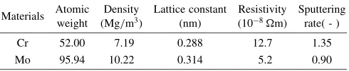
3.2 Resistivity
Mo concentration dependence of the resistivity on Cr-Mo alloy films is shown in Fig. 2. Resistivities of the films become lower in the range of 20–40 at%Mo compared with Cr film, and become the same level around 60 at%Mo, and become a little bit higher at 80 at%Mo, and then become lowest at Mo film. Resistivity of binary solid solution, whose elements belong to the same group in the periodic table, in general, shows Nordheim’s rule, that is, risistivity shows approximately parabolic shape with maximum value at about
equi-atomic composition.16)It is reported that resistivity of
bulk in Cr-Mo was measured and followed the rule up to
8 at%Mo.17)Resistivity being assumed the Nordheim’s rule is
shown with dotted line in Fig. 2, whose both ends (Mo and Cr) were assumed to be bulk values in Table 1 and the value at 8 at%Mo was assumed to be that of bulk measurement in reference 17). Comparison with resistivity of bulk pure metals makes us understand that the resistivity of the films indicate two times higher in Cr film and three times higher in Mo film. Higher resistivity of the films was caused by several kinds of defects in the film and surface. Although we did not
measure the resistivity within the range of 10 at%Mo, the decrease of the resisitivity of Cr-Mo films in the range of 20 and 60 at%Mo looks curious.
3.3 Stress of the film
The stress of the sputtered film was governed by internal
stress, which depends on sputtering condition.18) Mo
con-centration dependence of the stress in the Cr-Mo alloy films is shown in Fig. 3. The stress of Cr film is large tensile stress and that of alloy films become lower with increasing of Mo concentration. Thus the alloying Cr with Mo lowers stress of the Cr film.
3.4 Structure of the films
[image:2.595.332.522.70.300.2]XRD patterns were measured for prepared alloy films and indicate that crystal structure of all alloy films are bcc with strongly preferred-oriented (110). Preferred orientation of (110) is quite general because close packed planes are
Table 2 Mo concentration of Target materials and films deposited. Mo concentrations of the films were good agreement in the concentrations of target materials.
Mo concentration of Target (at%) 20 40 60 80
Mo concentration of film (at%) 21 42 63 81
8.0
8.5
9.0
9.5
10.0
Deposition r
ate
,
/ nm/sec
0
Mo concentration, C
/at%
100
80
60
40
20
r
Fig. 1 Deposition rates of Cr-Mo films against Mo concentrations. Deposition rate decreases monotonically with increasing Mo concentra-tion.
Film (measured value)
Bulk (Estimated value)
Resistivity
,
ρ
/10
-8
Ω
m
Mo concentration,
C
/at%
0
10
20
30
40
20
40
60
80
100
Fig. 2 Mo concentration dependence of resisitivity on Cr-Mo films. The resistivity of the film decreases up to 40 at%Mo and increases up to 80 at%Mo. The lowest resistivity was obtained in Mo film.
0
500
1000
1500
20
Mo concentration, C/at%
Stress
,
σ
/MP
a
100
80
60
40
[image:2.595.55.285.97.323.2] [image:2.595.323.528.365.520.2]stacked while deposition, in general, that is, (110) of bcc was
preferably oriented.19)
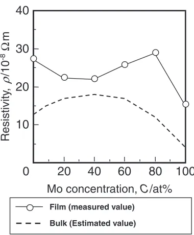
Lattice constants for the films were determined using (110) reflection by XRD. These data were compared with lattice
constants obtained from Vegard’s law.20) Lattice constants
[image:3.595.314.537.69.359.2]for Cr and Mo were refereed from bulk data. Mo concen-tration dependence of the lattice constants is shown in Fig. 4, which shows that observed values are smaller than calculated values. The differences between observed values and calculation values decrease with Mo concentration from 20 to 80 at% and increase again at Mo. In all concentration range, observed values are smaller than calculated values as mentioned above. Thus the residual tensile stress may be applied. FWHMs of (110) peak on Cr-Mo alloy films shown in Fig. 4 are broader than those of Cr and Mo films and indicate that Cr-Mo alloy films include strain. Expansion of the lattice constant with increase of Mo concentration reflects that larger atomic radius atoms, Mo atoms, were replaced with Cr atoms.
3.5 SEM and TEM Observations of Cr-Mo films
FE-SEM images of Cr-Mo films were shown in Fig. 5. The
observations were carried out from 45 of the film surface
normal. Thus the surface and cross-section are observed simultaneously. The area of observed point was focused on edge of the surface and cross-section. The structures of films are columnar and have surface relief along the column. The sizes of the columns in Cr films are approximately 50–60 nm and those of column in Mo films are smaller. The sizes of columns in Cr-Mo films increase with Mo concentration up to 60 at%Mo films. Boundaries between columns become diffuse. The sizes of columns in 80 at%Mo film are finer and similar to those of column in Mo film.
TEM images of films are shown in Fig. 6. Black and white tones represent crystal orientation difference. Grain sizes were estimated here to be small round shapes with same tone area. Grain sizes of Cr films are 25 nm and those of Mo films
are 15 nm. The grain sizes of Cr-Mo film shown in Fig. 7 with open circles are almost constant up to 40 at%Mo and decreases monotonically to Mo film. Further characteristics can be seen, that is, the grain structure of films looks like gathering the several grains. These grains formed the
Estimated value from Vegard’s law Observed data
FWHMs of (110)
Lattice constant,
/nm
Mo concentration,
C
/at%
0.285
0.290
0.295
0.300
0.305
0.310
0.315
0
0.38
0.40
0.42
0.44
0.46
0.48
0.50
0.52
100
80
60
40
20
FWHMs of (110) /
°
a
Fig. 4 Mo concentration dependence of lattice constant on Cr-Mo films. The lattice constants follow Vegard’s law.
Cr Cr20Mo
Cr60Mo
Cr80Mo Mo
Cr40Mo
Surface
Cross-section
Glass Substrate
Fig. 5 FE-SEM images of Cr-Mo films. The structures of films are columnar. The sizes of the columns are changes according to Mo concentration.
[image:3.595.56.282.71.296.2] [image:3.595.311.541.423.663.2]aggregated grain, whose sizes were estimated to be one of nearly tone. Those aggregated grain sizes are also shown in Fig. 7 with filled circles. The aggregated grain sizes increases up to 70 nm at 40 at%Mo and decreases gradually to 25 nm at Mo film. The sizes of columns in SEM observations were almost the same as aggregated grain sizes rather than the single grain sizes. Thus, the columns of films are composed of combined several grains.
4. Discussion
Structure of the films depend on conditions of sputtering such as substrate temperature, pressure of Ar, incident power of target, in general, and also depend on melting points of materials. The deposition conditions in this report are the same for all alloy films. It is well known that structure of films is classified into ZONE-1, ZONE-T, ZONE-2 and ZONE-3 depending on Ar pressure and the ratio of substrate
temperature and melting point of the material (Ts=TM).21)
Ts=TM of Cr film is 0.2 and that of Mo film is 0.15. The
microstructure of Cr, Mo, Cr-Mo alloy films look like ZONE-1 or ZONE-T from the cross-section view of Fig. 5. Melting points are considered for explaining the micro-structure. Grain sizes of Mo films are smaller than those of Cr films, corresponding to melting points; that is, melting point of Mo is higher than that of Cr. While grain sizes of Cr-Mo films are in between that of Cr films and Mo films as was indicated above, the aggregated grain sizes of Cr-Mo films are not in between that of Cr and Mo. Thus the process of forming the aggregated grain is considered below.
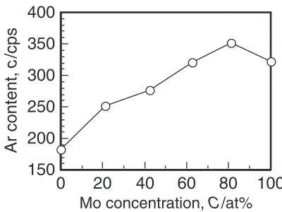
An effect of recoiled Ar, which is characteristics of sputtering method, is considered. Recoiled Ar atoms or ions are deposited on the films. It is reported that amount of
recoiled Ar increase for heavy atoms deposition.22)Amount
of Ar in the films was measured by EPMA and shown in Fig. 8. Amount of Ar increases with increase of Mo concentration, which follows the tendency mentioned above. Exception is found at Mo film, that is, amount of Ar in Mo films decreases. The Ar atoms were trapped in interstitial
sites of the film. Thus, the many Ar atoms had been taken in the alloy films easier than pure metal films. Recoiled Ar atoms release heat in the film, and released heat give the energy to atoms and make a rearrangement of atoms around boundaries. Thus wider grain boundary gaps become nar-rower than original one. This is the process of being produced aggregated grain.
Recoiled Ar atoms change the structure of Cr-Mo film from ZONE-1 to ZONE-T. Thus the strain of the structure was relaxed, and the relaxation of the structure decreases defects. Figure 9 shows the stress of Cr-Mo film against amount of Ar. The stress of the films decreases with increase of Ar content. It is considered that the peening effect of recoiled Ar is similar to the bias sputtering method.
Vegard’s law indicated that Mo atoms are replaced with Cr atoms by alloying. Replacements of Mo atoms by Cr make a possibility of relaxation of tensile stress. In the present case, however, Ar atoms must be the main reason of the stress relaxation as shown in Fig. 9. Where do Ar atoms locate or how to relax the stress? The recoiled Ar atoms assist rearrangement of grain boundaries creating aggregated grains. Those Ar atoms must be captured and located around boundaries. Location of Ar atoms around boundaries gives compressive force between aggregated grains and causes a decrease of tensile stress except for Mo film.
Gr
ain Siz
e
,
/nm
Mo concentration, C/at%
0
20
40
60
80
100
120
20
Aggregated grain Single Grain
100
80
60
40
d
Fig. 7 Grain sizes of Cr-Mo films against Mo concentrations. The aggregated grain sizes increase up to 40 at%Mo and decrease gradually to Mo.
150
200
250
300
350
400
Ar content,
c
/cps
0
Mo concentration,
C
/at%
100
80
60
40
20
Fig. 8 Ar contents of Cr-Mo films against Mo concentrations. The amount of Ar increases with increasing Mo concentration.
0
500
1000
1500
150
Ar content, c/cps
Stress
,
σ
/MP
a
400
350
300
250
200
[image:4.595.71.266.72.262.2] [image:4.595.322.529.281.434.2]Resistivity is caused by electron scattering with crystal defects such as impurities, grain boundaries. Grain sizes in bulk are larger than the mean free path of the electron and are less influence on the resistivity. Cr and Mo belong to the same Group VIB, and Cr-Mo alloy forms a solid solution in the phase diagram. The resistivities of Cr-Mo alloy films are affected by crystal defects. The aggregated grain sizes in the present films showed a correlation with resistivities, that is, larger aggregated grain sizes showed lower resistivity as shown in Fig. 6 and Fig. 7. Mean free path of electron in Cr is a few ten nm. The aggregated grain may work as a larger single grain. Aggregated grain sizes of Cr-Mo alloy films were from 15 to 70 nm. Thus the main reason of resistivity is the aggregated grain sizes in films, which are comparable with the mean free path of electron.
Recoiled Ar atoms must play an important role in Cr-Mo alloy films. However exception was found at Mo film. Further study is necessary to understand the phenomena found in Cr-Mo film completely.
5. Conclusions
Sputtered Cr-Mo alloy flims were investigated, which forms a solid solution belonging to the same Group VIB in the phase diagram.
(1) Lattice constants of alloy films were determined by XRD and showed a little bit smaller than the values from Vegard’s law. FWHMs of (110) reflection on the alloy films were broader than that of Cr and Mo film. (2) Resistivity against Mo concentration was obtained.
Resistivities of alloy films (20 and 40 at%Mo) show lower resistivity than Cr film.
(3) SEM and TEM images indicated that several grains were combined and form lager aggregated grains and columnar structure.
(4) Resistivity was strongly affected by aggregated grain sizes of films. Especially, resistivities between 20 and 60 at%Mo decrease because of aggregated gain sizes increase in this range.
(5) Mo concentration dependence of the stress was deter-mined. Higher tensile stress at Cr film decreased monotonically with increase of Mo concentration. (6) The stress of films depends on amount of Ar. Recoiled
Ar atoms must play an important role for the above sputtering behavior in Cr-Mo alloy films.
Acknowledgement
The authors are grateful for the experimental support from Metallurgical Research Laboratory of Hitachi Metals Ltd., Japan.
REFERENCES
1) E. Ando and S. Suzuki: J. Non-Cryst. Solid218(1977) 68–73. 2) K. K. Ho, C. E. Yong, H. S. Gyun, P. B. Gyu and Y. J. Hong: Surf. Coat.
Technol.201(2006) 4068–4072.
3) L. C. Hsia: J. Electrochem. Soc.131(1984) 2133–2137.
4) T. Takahashi: Electron. Parts Mater. extra number of July (2001) 62–68.
5) T. Yamada, N. Tani, M. Ishikawa, Y. Ota, K. Nakamura and A. Itoh: IEEE Trans. Magn. MAG-21 (1985) 1429–1431.
6) J. C. Allan and R. D. Fisher: IEEE Trans. Magn. MAG-23 (1987) 122–124.
7) M. A. Parker, J. K. Howard, R. Ahlert and K. R. Coffey: J. Appl. Phys. 73 2A (1993) 5560–5562.
8) M. Hayama: Semicond. World7(1991) 176–178 (in Japanese). 9) H. Tanaka: SID 1987 Digest (1987) pp 140.
10) ANELVA C-3900 series: Semicond. FPD World22(2003) 150 (in Japanese).
11) H. Murata: Hitachi-Metals Technology12(1996) 23–28 (in Japanese). 12) D. W. Hoffman and J. A. Thornton: Thin Solid Films 40 (1977)
355–363.
13) G. C. A. M. Janssen and J. D. Kamminga: Appl. Phys. Lett.85(2004) 3086–3088.
14) Metal data book 4th revised edition, (The Japan Inst. Metals: 2004) pp. 1–40 (in Japanese).
15) R. V. Stuart (Translated by M. Mouri and A. Kazusaka): Vacuum Techinology, Thin Films, and Sputtering, (GIHODO SHUPPAN Co.Ltd) pp. 112 (in Japanese).
16) The theory of the properties of Metals and Alloys, ed. by N. F. Mott and H. Jones, (Dover Publications, New York, 1958) 296–298.
17) S. Arajs, E. E. Anderson and K. V. Rao: J. Less-Common Metals26
(1971) 157–164.
18) D. W. Hoffman and J. A. Thornton: J. Vac. Sci. T.20(1982) 355–358. 19) A. Kinbara:SPUTTERING, (University of Tokyo Press. 1984) pp. 181
(in Japanese).
20) C. Barrett and T. B. Massalski:Structure of Metals 3rd Revised Edition Pergamon, (1980) pp. 372.
21) J. A. Thornton: J. Vac. Sci. T.11(1974) 666–670.
22) J. A. Thornton, J. Tabock and D. W. Hoffman: Thin Solid Films64
![[Rb(18 crown 6)][Rb([2 2 2] cryptand)]Rb2Sn9·5NH3](data:image/gif;base64,R0lGODlhAQABAIAAAP///wAAACH5BAEAAAAALAAAAAABAAEAAAICRAEAOw==)