ORIGINAL PAPER
AbstractThe spatial coherence of organic light-emitting diodes (OLEDs) is an important parameter that has gained little atten-tion to date. Here, we present a method for making quantitative measurements of the spatial coherence of OLEDs using a Young’s double-slit experiment. The usefulness of the method is demonstrated by making measurements on a range of OLEDs with different emitters (iridium and europium complexes) and architectures (bottom and top emitting) and the fringe visibil-ity is further manipulated by gratings embedded in external diffractive optical elements. Based on the experiments and simulation of the results, we quantitatively determine the spatial coherence lengths of several OLEDs and find them to be a few micrometers. A 60% increase in the spatial coherence length was observed when using a narrow bandwidth emitter and a metal-coated grating.
Measuring and structuring the spatial coherence length
of organic light-emitting diodes
Guohua Xie
1, Mingzhou Chen
2, Michael Mazilu
2, Shuyu Zhang
1,3, A.K. Bansal
1,
Kishan Dholakia
2, and Ifor D. W. Samuel
1,∗1. Introduction
Organic light-emitting diode (OLED) technology has at-tracted great attention due to its promising applications in lighting and displays [1–14]. Recently, new applica-tions of this technology in visible-light communication and biomedical instruments suggest that OLEDs will be universal in the next generation of photonic devices [ 15–18]. For such emerging applications, the coherence of the beam and the ability to make it directional are of in-terest. OLEDs are compact, versatile, potentially low-cost and visible sources. Though many aspects of the electri-cal and optielectri-cal properties of OLEDs have been studied in the last 25 years [7, 19–21], the spatial coherence has received very little attention. The microcavity-like struc-tures used in OLEDs pave the way for optical manage-ment and manipulation [22–27]. This makes them ideal alternative light sources for portable and disposable instru-ments for biomedical applications such as photodynamic
1Organic Semiconductor Centre, SUPA, School of Physics and Astronomy, University of St Andrews, North Haugh, St Andrews, KY16 9SS, UK 2SUPA, School of Physics and Astronomy, University of St Andrews, North Haugh, St Andrews, KY16 9SS, UK
3Present address: School of Information Science and Technology, Fudan University, North Haugh, Shanghai 200433, China
∗Corresponding author: [email protected]
This is an open access article under the terms of the Creative Commons Attribution License, which permits use, distribution and reproduction in any medium, provided the original work is properly cited.
therapy for skin-cancer treatment [18]. In this context, the spatial coherence of a light source is important for being able to shape and direct the emission beam – for example the wavefront of a beam of sufficient spatial coherence can be shaped by a spatial light modulator. The coherence also plays a large role in the penetration of light into living tissues [28–30].
SCHEME 1 The optical setup used to mea-sure fringe visibility and hence determine spatial coherence. The route to extracting the spatial coherence length,lsc, is also il-lustrated.
showing that after spatial filtering of an OLED, clear fringes can be obtained, but they do not directly measure the spatial coherence of the OLED. Similarly, Saxena et al. followed this method to investigate the spatial coherence from a tris-(8-hydroxyquinoline) aluminum (Alq3)-based
OLED. However, a limitation of these studies is that they measured the spatial coherence properties of a spatially filtered OLED, rather than the light source itself.
In this paper, we report measurements of the intrinsic spatial coherence length of a range of OLEDs by introduc-ing a Fourier transform imagintroduc-ing system, i.e. a 4f system. To improve the low visibility of the fringe from the OLEDs, we laterally integrated the OLEDs with external diffractive optical elements (DOEs) that consisted of submicrometer-scale gratings fabricated by UV-nanoimprint lithography (UV-NIL).
2. Methods and devices
2.1. The optical setup and the method to extract
the spatial coherence length
Scheme 1 illustrates the optical setup for measuring the spatial coherence of a light source. The light source was located in the focal plane of the objective lens. In order to have the best detection system for light of low coherence, we combined a double slit (125 μm separation) with a telescope with 40×magnification factor that will be able to detect the interference fringes of a light source having a spatial coherence length on the several-μm scale. A cooled CCD camera (SBIG, 3326×2504 pixels and 5.4×5.4μm2
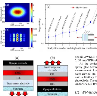
each pixel) was used to capture the fringes. We performed tests to verify the response of our experiment to a wide range of degrees of spatial coherence. To do this we replaced the OLED (see Scheme 1) by a He-Ne laser illuminating a rotating diffuser coated with varying numbers of layers of layers of scattering films (sticky tape). The beam of the He-Ne laser was expanded by a 60× objective lens and then collimated by incorporating another lens with a focal length of 150 mm. A variable single slit was inserted between the rotating diffuser and the collimating lens to control the beam size. Figure 1a shows the fringes of the light beam passing through a rotating diffuser that consists of 2 outer sticky films (tesafilm) /glass/2 inner sticky films. No clear interference pattern can be observed in Fig. 1a as the phase of the laser beam was completely scrambled by the rotating diffuser. In contrast, the light beam from the He-Ne laser without passing through the diffuser exhibits very clear interference patterns. We used a two-dimensional fast Fourier transform (2D-FFT) to determine and average the visibility of the fringes from our low-coherence light sources. In Fig. 1c, the fringe visibility was plotted by changing the number of sticky films attached to the glass and adjusting the opening of the variable single slit. Using this apparatus, very low visibility (defined in section 2.4) down to 0.02 can be measured.
2.2. OLED fabrication and characterization
Figure 1 Fringes captured by the CCD camera (a) with 2 outer films/glass/2 inner films as the ro-tating diffuser and (b) without the diffuser. (c) Fringe visibility changes with different rotating diffuser used. The outer film (OF), glass (G), the inner film (IF) relative to the rotating diffuser’s position (see the inset) and the opening size of the single slit are also indicated.
Figure 2 The architectures of bottom- (a) and top-emitting (b) OLEDs.
spin coating of the organic layers and evaporation of the electrodes. The structure of our bottom-emitting OLED (shown in Fig. 2a) with an Ir emitter was glass/ITO p-doped HTL(30 nm)/N,N -di(naphthalene-2-yl)-N,N-diphenyl-benzidine (α-NPD, 10 nm)/α-NPD doped with 10 wt% iridium(III) bis(2-methyldibenzo-[f,h]chinoxalin)(acetylacetonate) (Ir(MDQ)2(acac), 20 nm)
/bis-(2-methyl-8-quinolinolato)-4-(phenyl-phenolato) alu-minum(III) (BAlq2, 10 nm)/n-doped ETL (40 nm)/Al
(100 nm). HTL and ETL denote hole- and electron-transporting layers, respectively. The architecture of the top-emitting OLED (shown in Fig. 2b) with the Ir emitter was glass/Al (40 nm)/Ag (40 nm)/p-doped HTL (50 nm)/α -NPD doped with 10 wt% Ir(MDQ)2(acac) (10 nm)/BAlq2
(10 nm) /n-doped ETL (40 nm)/Al (1 nm)/Ag (18 nm). The structure of the bottom-emitting Eu emitter was similar to that of the devices with an Ir emitter, i.e. glass/ ITO/poly(3,4-ethylenedioxythiophene):poly(styrenesulfo-nate) (PEDOT:PSS, 30 nm)/poly(N-vinylcarbazole) (PVK, 30 nm)/4,4-N,N-dicarbazole-biphenyl (CBP):2-(tert-butylphenyl)-5-biphenylyl-1,3,4-oxadiazole (PBD):tris(di-benzoylmethane)mono (4,7-diphenylphenanthroline)euro-pium(III) (Eu(DBM)3Bphen) (65:30:5, 30
nm)/1,3,5-tris(2-N-phenylbenzimidazolyl)benzene (TPBi, 40 nm)/ Ca (20 nm)/Al (100 nm). The top-emitting OLED stack with the Eu emitter was glass/Ag (80 nm)/ PEDOT:PSS
(30 nm)/PVK(30 nm)/CBP:PBD:Eu(DBM)3Bphen (65:30:
5, 30 nm)/TPBi (40 nm)/Ca (2 nm)/Ag (18 nm).
All the devices were encapsulated with UV-curable epoxy glue before being taken out of the glove-box for measurement. Luminance–current–voltage measurements were carried out using a Keithley 2400 source measure unit, a Keithley 2000 multimeter and a calibrated silicon photodiode. The spectrum was collected by a fiber-coupled Andor DV420-BV CCD spectrometer.
2.3. UV-Nanoimprint lithography (UV-NIL)
UV-NIL was used to make large-area micrometer and nanometer scale patterns [33]. Before transfer-ring a thick layer of perfluoropolyether(PFPE)-urethane dimethacrylate (Fluorolink MD700) as a compliant mate-rial onto a clean and bare silicon substrate, an adhesive layer of (3-Trimethoxysilyl)propyl acrylate (Sigma-Aldrich) was spin coated directly onto the glass substrate after oxygen plasma treatment. Another layer of MD700 was spin coated on the glass substrate after UV exposure for 220 s. Through the second UV exposure, the 1D grating pattern with a pe-riod of 350 nm on a Si master was transferred onto this glass substrate (daughter stamp) by adding some droplets of perfluoroalkylpolyether (Fluorolink MD500) mixed with 1–2% of the photoinitiator DURACOUR.
The daughter stamp was used as a mold for replicat-ing the gratreplicat-ing structures onto a photoresist (Micro Resist Technology UVCur06) that was spin coated atop another bare glass substrate with an additional adhesion promoter (Micro Resist Technology mr-APS1). The UV nanoimprint lithography (UV-NIL) processes were performed using an EVGR620 automated mask alignment system. The grating profile was imaged by a Hitachi S-4800 scanning electron microscope (SEM).
2.4. Simulation of the spatial coherence length
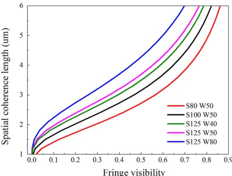
Figure 3 Simulated spatial coherence length as a function of the fringe visibility, considering different separation (S inμm) and width (W inμm) of the double slit used in the setup shown in Scheme 1.
corresponding to a light source being incoherent to fully coherent. In order to relate the spatial coherence length to the fringe visibility quantitatively, we used a numerical simulation. A partially coherent beam can be described by the Gaussian–Schell model correlator,
μ(ρ1,ρ2)=exp
−| ρ1− ρ2|2
L2c
, (1)
where ρ1 and ρ2 are the vectors denoting two different
points on the transverse plane that is perpendicular to the beam propagation direction, andLcis the transverse
coher-ence length [34]. We then simulate the passage of such a partially coherent beam through any optical system, such as a telescope or a double slit, by propagating the beam with the method of ABCD ray matrices [35]. With this numeri-cal method, we can purposely simulate our optinumeri-cal system as shown in Scheme 1. From the interference pattern, we can calculate the fringe visibility as,
V = Imax−Imi n Imax+Imi n
, (2)
whereImaxandIminare the peak intensities of the upper and
lower envelopes of the measured fringes. For our particular application, we need to modify this equation to calculate the modified fringe visibility due to the high noise level and low visibility. In a similar way to other fringe-analysis techniques, a Fourier transform was applied to the original fringe pattern, and the visibility calculated in the Fourier domain as,
VFFT=
P1
P0,
(3)
where P0 is the area under the zeroth order peak, andP1
is the sum of the areas under the two first-order peaks in the Fourier domain. The results of the simulation relating
3. Results and discussion
3.1. The electrical and optical properties of the
OLEDs
The iridium complex-based bottom-emitting OLED (Ir-BEOLED) exhibited a very low turn-on voltage of 2.1 V at a luminance of 1 cd/m2 and a high luminance of
10 000 cd/m2at 4.0V (see Figs. 4a and b). From Fig. 4c, a
full width at half-maximum (FWHM) of the EL spectrum at 1 mA was determined to be 79.4 nm and the peak wave-length was 609 nm. Similarly, the iridium complex-based top-emitting OLED (Ir-TEOLED) has a turn-on voltage of 2.3 V contributed to the use of the electrically doped charge transporting layers [36]. However, the luminance reached 10 000 cd/m2at around 4.8 V ascribed to the different op-tical cavity effect and outcoupling property, which led to a FWHM of 72.5 nm and peak emission at 625 nm.
Unlike the iridium complex-based devices, the Eu complex-based devices (Eu-BEOLED and Eu-TEOLED) showed much higher driving voltages and lower luminance resulted from less conductive charge transporting layer used (Figs. 5a and b). Nevertheless, this Eu complex exhibited a very narrow emissive bandwidth as a result of the charac-teristic emission from the Eu3+ ion based on the5D
0–7F2
transition, which makes it an ideal candidate for the pure red devices [37]. Therefore, we observed small FWHMs of 5.6 nm and 5.5 nm and peak emission both at 611 nm (shown in Fig. 5c), corresponding to BEOLED and Eu-TEOLED, respectively.
3.2. The spatial coherence measurements
of OLEDs
[image:4.594.56.289.74.251.2]Figure 4 Current density–voltage (a) and luminance–voltage (b) char-acteristics and the EL spectrum at 1 mA (c) of the Ir complex-based bottom- and top-emitting OLED (Ir-BEOLED and Ir-TEOLED).
Figure 5 Current density–voltage (a) and luminance–voltage (b) char-acteristics and the EL spectrum at 1 mA (c) of the Eu complex-based bottom- and top-emitting OLED (Eu-BEOLED and Eu-TEOLED).
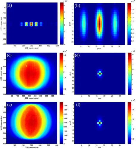
separation 125μm) the spatial coherence lengths of Ir- and Eu-BEOLEDs can be deduced from Fig. 3 to be 1.6±0.1 and 1.7±0.1μm.
For the top-emitting OLEDs, we obtained visibilities of the fringes (see Figs. 7a and c) of 0.07±0.01 and 0.11
±0.02 for the Ir and Eu emitter-based devices, respectively (Figs. 7b and d). Therefore, the top-emitting Ir and Eu emitter-based devices exhibited slightly enhanced spatial coherence lengths of 1.73±0.06 and 1.9±0.1μm, com-pared to the bottom-emitting counterparts. The lower vis-ibility of the Ir complex-based devices arises from their broader emission spectrum, which leads to overlapping fringe patterns for different wavelengths.
3.3. Structuring the spatial coherence
of BEOLEDs with a DOE
To manipulate the light beams from OLEDs for phase con-trol, we need to increase the spatial coherence. Theoretical
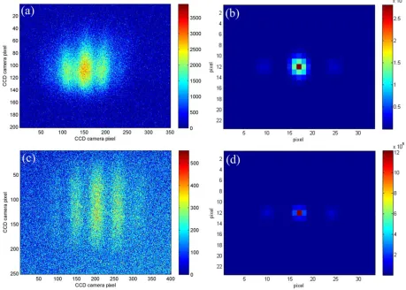
Figure 6 Fringes of He-Ne laser (a), Ir-BEOLEDs (c) and Eu-BEOLED (e). 2D-FFT Patterns of the fringes of He-Ne laser (b), Ir-BEOLEDs (d) and Eu-BEOLED (f).
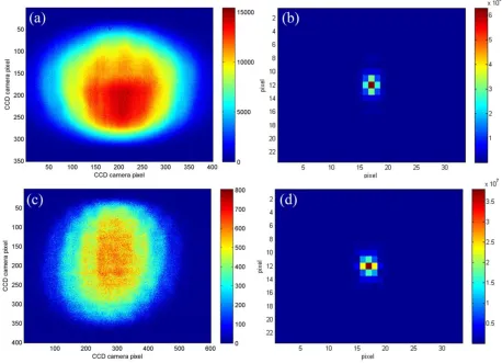
To characterize the spatial coherence, the emission from the DOE was coupled into the telescope (see Scheme 1) and the fringes of iridium and europium complex-based devices captured by the CCD camera are plot-ted in Figs. 9a and c. This gave by far the clearest in-terference patterns of the devices studied in this paper. The fringe visibility of Ir and Eu complex-based BE-OLEDs were 0.20 ±0.03 and 0.34 ±0.04, respectively.
Figure 7 Fringes of TEOLEDs based on Ir (a) and Eu (c) complexes as the emitters. (b) and (d) are the corresponding 2D-FFT patterns.
Figure 8 (a) Comparison of the calculated optical-mode contributions of BEOLED and TEOLED. (b) The schematic diagram of the laterally integrated BEOLED and DOE and the outcoupled light beams for the spatial coherence measurement. The inset above the DOE is an SEM image of the grating on the glass substrate.
4. Conclusion and outlook
We have constructed an optical setup composed of a tele-scope and a Young’s double slit to determine the spatial coherence of OLEDs. This was used to perform a
[image:7.594.69.525.460.614.2]Figure 9 Fringes of the emission from DOE connected to BEOLEDs based on Ir (a) and Eu (b) complexes as the emitters.
Figure 10 Summary of the spatial coherence lengths of OLEDs measured using the double slit experiment.
visibility was gradually improved from 0.05 to 0.34. Due to the broad emission of the Ir complex, the devices exhib-ited relatively low fringe visibility and thus small spatial coherence lengths with weak microcavity effect. The spa-tial coherence lengths of a europium complex-based OLED
was improved from1.7 to1.9μm by changing the stack architecture from bottom emitting to top emitting. Another 44% improvement can be achieved by employing an ex-ternal DOE. In the future it should be possible to achieve higher spatial coherence by deliberately coupling out an individual optical mode with a suitable grating structure. Our results pave a novel path for optical management in organic light sources for visible-light communication and biomedical applications.
Acknowledgements. This work was supported by the Engi-neering and Physical Science Research Council (EPSRC) grants “Challenging the limits of photonics: structured light” EP/J01771X and “Ultra-parallel visible light communications” EP/K00042X. IDWS and KD also acknowledge Royal Society Wolfson Research Merit awards. The research data supporting this paper can be ac-cessed at http://dx.doi.org/10.17630/73b69cb8-ba6c-4d71-9985-e723e932c337.
Received:15 March 2015,Revised:17 September 2015, Accepted:28 September 2015
Published online:30 November 2015
[image:8.594.61.284.447.631.2]References
[1] S. Reineke, F. Lindner, G. Schwartz, N. Seidler, K. Walzer, B. Lussem, and K. Leo, Nature 459, 234–238 (2009).
[2] G. Xie, Q. Xue, P. Chen, C. Tao, C. Zhao, J. Lu, Z. Gong, T. Zhang, R. Huang, H. Du, W. Xie, J. Hou, Y. Zhao, and S. Liu, Org. Electron.11, 407–411 (2010).
[3] J. Blochwitz-Nimoth, O. Langguth, S. Murano, G. He, T. Romainczyk, and J. Birnstock, Journal of the Society for Information Display,18, 596–605 (2010).
[4] C. Adachi, M. A. Baldo, M. E. Thompson, and S. R. Forrest, J. Appl. Phys.90, 5048–5051 (2001).
[5] R. H. Friend, R. W. Gymer, A. B. Holmes, J. H. Burroughes, R. N. Marks, C. Taliani, D. D. C. Bradley, D. A. D. Santos, J. L. Bredas, M. Logdlund, and W. R. Salaneck, Nature397, 121–128 (1999).
[6] J. Kido, M. Kimura, and K. Nagai, Science267, 1332–1334 (1995).
[7] C. W. Tang and S. A. VanSlyke, Appl. Phys. Lett.51, 913– 915, (1987).
[8] M. A. Baldo, D. F. O’Brien, Y. You, A. Shoustikov, S. Sibley, M. E. Thompson, and S. R. Forrest, Nature395, 151–154 (1998).
[9] X. Gong, S. Wang, D. Moses, G. C. Bazan, and A. J. Heeger, Adv. Mater.17, 2053–2058 (2005).
[10] H. T. Nicolai, A. Hof, and P. W. M. Blom, Adv. Funct. Mater. 22, 2040–2047 (2012).
[11] C.-W. Chen, Y.-J. Lu, C.-C. Wu, E. H.-E. Wu, C.-W. Chu, and Y. Yang, Appl. Phys. Lett.87, 241121 (2005).
[12] F. A. Boroumand, P. W. Fry, and D. G. Lidzey, Nano Lett. 5, 67–71 (2005).
[13] P. L. Burn, S. C. Lo, and I. D. W. Samuel, Adv. Mater.19, 1675–1688 (2007).
[14] S. C. Lo, N. A. H. Male, J. P. J. Markham, S. W. Magennis, P. L. Burn, O. V. Salata, and I. D. W. Samuel, Adv. Mater. 14, 975–979 (2002).
[15] P. A. Haigh, Z. Ghassemlooy, H. Le Minh, S. Rajbhandari, F. Arca, S. F. Tedde, O. Hayden, and I. Papakonstantinou, J. Lightwave Technol.30, 3081–3088 (2012).
[16] R. M. Owens and G. G. Malliaras, MRS Bull.35, 449–456 (2010).
[17] J.-C. G. B¨unzli, S. Comby, A.-S. Chauvin, and C. D. B. Vandevyver, J. Rare Earths25, 257–274 (2007).
[18] S. K. Attili, A. Lesar, A. McNeill, M. Camacho-Lopez, H. Moseley, S. Ibbotson, I. D. W. Samuel, and J. Ferguson, Brit. J. Dermatol.161, 170–173 (2009).
[19] K. Walzer, B. Maennig, M. Pfeiffer, and K. Leo, Chem. Rev. 107, 1233–1271 (2007).
[20] G. M. Farinola and R. Ragni, Chem. Soc. Rev.40, 3467– 3482 (2011).
[21] Y. Shirota and H. Kageyama, Chem. Rev.107, 953–1010 (2007).
[22] D. P. Puzzo, M. G. Helander, P. G. O’Brien, Z. Wang, N. Soheilnia, N. Kherani, Z. Lu, and G. A. Ozin, Nano Lett.11, 1457–1462 (2011).
[23] C.-L. Lin, H.-W. Lin, and C.-C. Wu, Appl. Phys. Lett.87, 021101 (2005).
[24] J. R. Tischler, M. S. Bradley, V. Bulovi´c, J. H. Song, and A. Nurmikko, Phys. Rev. Lett.95, 036401 (2005).
[25] V. Bulovi´c, V. B. Khalfin, G. Gu, P. E. Burrows, D. Z. Garbu-zov, and S. R. Forrest, Phys. Rev. B58, 3730–3740 (1998). [26] S. Tokito, T. Tsutsui, and Y. Taga, J. Appl. Phys.86, 2407–
2411 (1999).
[27] N. Christogiannis, N. Somaschi, P. Michetti, D. M. Coles, P. G. Savvidis, P. G. Lagoudakis, and D. G. Lidzey, Adv. Opt. Mater.1, 503–509 (2013).
[28] T. Berki, P. N´emeth, and J. Heged¨us, Lasers Med. Sci.3, 35–39 (1988).
[29] D. Fixler, H. Duadi, R. Ankri, and Z. Zalevsky, Lasers Surg. Med.43, 339–343 (2011).
[30] H. Subramanian, P. Pradhan, Y. L. Kim, and V. Backman, Phys. Rev. E75, 041914 (2007).
[31] F. J. Duarte, L. S. Liao, and K. M. Vaeth, Opt. Lett. 30, 3072–3074 (2005).
[32] K. Saxena, D. S. Mehta, R. Srivastava, and M. N. Ka-malasanan, Appl. Phys. Lett.89, 061124 (2006).
[33] G. Tsiminis, Y. Wang, A. L. Kanibolotsky, A. R. Inigo, P. J. Skabara, I. D. W. Samuel, and G. A. Turnbull, Adv. Mater. 25, 2826–2830 (2013).
[34] Y. Yang, M. Chen, M. Mazilu, A. Mourka, Y. Liu, and K. Dholakia, New J. Phys.15, 113053 (2013).
[35] P. A. B´elanger, Opt. Lett.16, 196–198 (1991).
[36] G. Xie, K. Fehse, K. Leo, and M. C. Gather, Org. Electron. 14, 2331–2340 (2013).
[37] T. W. Canzler and J. Kido, Org. Electron.7, 29–37 (2006). [38] T. Saastamoinen and H. Lajunen, Opt. Lett.38, 5000–5003
(2013).
[39] S. Zhang, G. A. Turnbull, and I. D. W. Samuel, Appl. Phys. Lett.103, 213302 (2013).
[40] R. R. Chance, A. Prock, and R. Silbey, Adv. Chem. Phys. 137, 16 (1978).