Electron mobility in CdO films
S. K. Vasheghani Farahani, T. D. Veal, P. D. C. King, J. Zúñiga-Pérez, V. Muñoz-Sanjosé, and C. F. McConville
Citation: Journal of Applied Physics 109, 073712 (2011); doi: 10.1063/1.3562141
View online: http://dx.doi.org/10.1063/1.3562141
View Table of Contents: http://scitation.aip.org/content/aip/journal/jap/109/7?ver=pdfcov
Electron mobility in CdO films
S. K. Vasheghani Farahani,1T. D. Veal,1,a)P. D. C. King,2J. Zu´n˜iga-Pe´rez,3 V. Mun˜oz-Sanjose´,4and C. F. McConville1,b)
1
Department of Physics, University of Warwick, Coventry CV4 7AL, U. K.
2
School of Physics and Astronomy, University of St Andrews, St Andrews KY16 9SS, U. K.
3
Centre de Recherche sur l’He´te´ro-Epitaxie et ses Applications, Centre National de la Recherche Scientifique, Parc de Sophia Antipolis, Rue Bernard Gre´gory, 06560 Valbonne, France
4
Departamento de Fisica Aplicada y Electromagnetismo, Universitat de Vale´ncia, C/Dr. Moliner 50, 46100 Burjassot, Spain
(Received 31 January 2011; accepted 9 February 2011; published online 6 April 2011)
Electron mobility in degenerate CdO thin films has been studied as a function of carrier concentration. The “optical” mobility has been determined from infrared reflectance measurements of the conduction band plasmon lifetime. The acquired values vary from 209 to 1116 cm2 V1 s1 for carrier
concentrations between 2:51020and 2:61019cm3. Ionized impurity scattering is shown to be the
dominant effect reducing the intra-grain mobility of the electrons at room temperature. The transport mobilities from Hall effect measurements range between 20 and 124 cm2 V1 s1 which are
much lower than the optical mobilities. Simulation of grain boundary scattering-limited mobility is commonly based on models that assume a depletion layer at the boundaries which causes an inter-grain potential barrier. These models are found not to be applicable to CdO as it has been previously shown to have surface electron accumulation. Therefore, simulation of the transport mobility has been performed using the Fuchs-Sondheimer and Mayadas-Shatzkes models to take into account the grain boundary and surface scattering mechanisms, in addition to intra-grain scattering. The results indicate that electron scattering at grain boundaries with95 % reflection is the dominant mechanism in reducing the mobility across the layer. The effect of surface scattering plays only a minor role in electron transport.VC 2011 American Institute of Physics. [doi:10.1063/1.3562141]
I. INTRODUCTION
Carrier transport in semiconductors is of great impor-tance, from studying fundamental physical phenomena to their application in optical and electronic devices. The opera-tion of a transparent conducting oxide (TCO) is based on the band structure-related physical quantities, such as bandgap and bandedge effective mass, as well as the carrier collisions within the material represented by the corresponding carrier lifetimes for elastic scattering. CdO is a group II-VI transpar-ent conductor possessing a relatively low bandgap and high bulk conductivity relative to other TCOs. Koffyberg1studied the Hall mobility of CdO and suggested that scattering by ionized donors may be the dominant process in limiting the mobility. Indeed, it can be deduced from the recent work by Speaks et al.2 that, for carrier concentrations well below 51020 cm3 which corresponds to the Fermi level
stabili-zation of CdO, donor defects are dominant.
Yan et al.3 investigated the mobility of CdO samples with different Sn-doping levels in which the effect of ionized impurity and grain boundary scattering was suggested to play the major role in electron transport. On the other hand, several authors4–6have studied the transport mobility by tak-ing into account the grain boundary scattertak-ing for nondegen-erate and degennondegen-erate7 semiconductors based on Seto’s model8 wherein a depletion layer exists at the boundaries. CdO, having donor-type surface states and an accumulation
layer9 at the grain boundaries, cannot be analyzed by the aforementioned methods. Therefore, we have applied the Fuchs-Sondheimer (FS)10,11 and Mayadas-Shatzkes (MS)12 models to understand the nature of scattering mechanisms in our degenerate CdO samples.
II. EXPERIMENTAL DETAILS
In this work, cadmium oxide layers with (001) orienta-tion were grown onr-plane sapphire at atmospheric pressure by metal-organic vapor-phase epitaxy in which the precur-sors for oxygen and cadmium were tertiary butanol and dimethylcadmium respectively. The optoelectronic proper-ties of degenerate CdO have been studied for as-grown sam-ples and after reducing the carrier concentration, nb, by
annealing in vacuum at 400oC for 2 to 24 hrs.
Optical measurements were performed using a Bruker Vertex 70v Fourier-transform infrared spectrometer over the energy range 0.1 to 2.7 eV. Both the transmittance and reflectance of the samples were measured using an incident angle of 11 degrees with respect to the surface normal while maintaining the same optical path length. This allowed the conversion of transmission in the visible region to absorp-tion spectra without requiring assumpabsorp-tions concerning the energy dependence of the optical reflectance, as is com-monly the case. Hall effect, based on the standard Van der Pauw configuration, was used to obtain the sheet density,
ns, and transport mobility of the CdO samples. Both the
optical and Hall effect measurements were carried out at room temperature.
a)Electronic mail: [email protected]. b)Electronic mail: [email protected].
X-ray diffraction (XRD) and atomic force microscopy (AFM) measurements have been performed, before and after annealing, for structural characterization. The full width at half maximum of the CdO 002 rocking curve was in the range of 0.27–0:29 for the investigated samples, indicating a threading dislocation density of the order of 24109
cm2.13,14 This also implies that the density of dislocations in the samples is independent of the annealing treatment per-formed after growth. In the AFM images, pyramidal grains several hundreds of nanometers in size were observed which are similar to those previously reported for samples grown by the same method.15
III. DATA, SIMULATION, AND ANALYSIS
A. Bandgap and bandedge effective mass
Infrared (IR) reflectance of epitaxial CdO onr-plane sap-phire within an energy range of 100 to 900 meV for three dif-ferent carrier concentrations is shown in Fig.1. The energy corresponding to minimum reflectance, which is related to the conduction band plasma resonant energy, increases with car-rier concentration. In order to model the spectra, a three layer stratified medium (vacuum/CdO/sapphire) with coherent inter-ference16 has been considered. The two oscillator model of the complex dielectric function is used for the CdO layer, while the factorized model was applied for the sapphire sub-strate.17 The high frequency dielectric constant, eð1Þ, for CdO was set to 5.318which is consistent with a recent investi-gation of optical constants of CdO over a range of energies.19 The high frequency dielectric constant of 3.06 was used for sapphire.20Simulation of the data, as shown in Fig.1, allowed the determination of the plasma resonant energy and broaden-ing, and the film thickness,d. The carrier concentration of the
samples was calculated via, n¼ns=d, which varies between
2:61019and 2:51020cm3.
By analyzing the evolution of plasma energy and optical absorption edge with carrier density by performing model carrier statistics calculations employing a k.p nonparabolic dispersion21and bandgap renormalization effects, the funda-mental bandgap and bandedge effective mass were found to be 2.20 eV and 0:24m0, respectively. These are similar to
the results of an earlier investigation by Jefferson et al.
which included some of the same samples investigated here.22 The small differences are attributed to the larger range of bulk carrier densities and more accurate determina-tion of the absorpdetermina-tion coefficient utilized here.
B. Optical mobility
Broadening of the plasma edge obtained from mid-IR re-flectance simulations has been used to determine the optical carrier lifetime, s. The optical mobility of each sample has been calculated using optical carrier lifetime and the density of states averaged effective mass of conduction electrons,
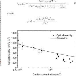
hmi, according to the equation,lopt ¼es=hmi. The results
versus carrier concentration are plotted in Fig.2which show that the optical mobility varies between 209 cm2 V1 s1
for the highest and1116 cm2V1s1for the lowest carrier
concentrations. With increasing carrier concentration, the broadening of the plasma edge increases as seen in Fig. 1 which corresponds to the reduction of the optical carrier life-time. This phenomenon causes the optical mobility to decrease with carrier concentration as shown in Fig.2.
The degenerate form of the Brooks-Herring formula23 has been used to simulate the ionized impurity scattering-limited mobility of the samples as a function of carrier concentration:
lion;deg¼
24p3ðe
se0Þ2h3n e3m2N
ion ln½1þyðnÞ yðnÞ
1þyðnÞ
h i; (1)
where,
yðnÞ ¼2ð3np 8Þ1=3
h2ese0
e2m ;
[image:3.612.56.300.474.731.2]FIG. 1. (Color online) Mid-IR reflectance spectra (open circles) and respec-tive simulations (solid lines) of three CdO samples with different carrier concentrations and lifetimes.
FIG. 2. Optical mobility of CdO and simulation of the ionized impurity scattering-limited mobility.
[image:3.612.292.556.475.740.2]where m is the density of states averaged effective mass, and Nion is the density of ionized impurities. The highest
Fermi energy of the samples investigated is0:48 eV above the conduction band minimum (CBM) while the Fermi level stabilization energy or charge neutrality level of CdO lies 1 eV above CBM.2 Therefore, Nion in Eq. (1) has been
approximated by the density of ionized donors. The ionized donors have been assumed to be singly charged. The simula-tion of the optical mobility data points is represented in Fig.2. The results show that ionized impurity scattering is the dominant scattering mechanism reducing the optical mo-bility in degenerate CdO at room temperature. The effect of lattice scattering on the mobility was found to be negligible.
C. Transport mobility
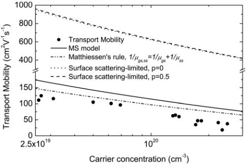
The transport mobility of degenerate CdO samples measured by the Hall effect varies between20 and124 cm2 V1 s1 for the highest and lowest carrier concentra-tions, respectively, as shown in Fig.3. It is apparent that the transport mobility is significantly lower than the optical mo-bility of the electrons for all the samples. Therefore, during Hall effect measurements of the transport mobility, the con-duction electrons must experience one or more additional scattering mechanisms. While during transport measure-ments the electrons traverse the film in response to the applied bias, optical excitation during IR reflectance results in no such phenomenon. This suggests that grain boundary scattering and/or surface scattering are responsible for the transport mobility being much lower than the optical mobil-ity. This interpretation is justified by the following quantita-tive modeling of these electron scattering mechanisms.
Commonly, the effect of grain boundaries on carrier transport mobility has been studied based on inter-grain bar-riers resulting from boundary trap states which are indicative of depletion layers at the boundaries. Simulation of the trans-port mobility under such conditions is based on the model proposed by Seto8for nondegenerate semiconductors. Under the same boundary conditions with degenerate intra-grain
characteristics, the modified expression for grain boundary scattering-limited mobility incorporating Fermi-Dirac statis-tics is used which predicts that the transport and optical mo-bility will merge as the barrier becomes surmountable by increasing the carrier concentration and therefore the Fermi level. However, as can be seen in Figs.2and3, the two sets of data points do not merge at higher carrier concentrations. This suggests that this approach to grain boundary scattering is not appropriate here.
Indeed, previous investigations have shown that CdO has a surface accumulation layer.9Therefore, we expect that there exists an electron accumulation at the grain boundaries and dislocation lines within the films. This has been imple-mented in the modeling of the grain boundary scattering. In order to simulate the transport mobility of the CdO samples, we therefore additionally considered scattering by grain boundaries and surfaces making use of the MS model12 to-gether with the FS theory of scattering at surfaces which apply to a degenerate electron gas.10,11It is worthy of men-tion that from the analysis of the optical absorpmen-tion and mid-IR reflectance data, it is apparent that there exists a Burstein-Moss shift for all the CdO samples investigated, indicating the relevance of considering the conduction electrons as a degenerate electron gas. This feature and the aforementioned electron accumulation make these models applicable to sim-ulate the data.
Firstly, the effect of surface scattering has been modeled according to the equation:11
lss¼l0 1
3
2kð1pÞ
ð1
1
1
t3
1
t5
1ekt
1pektdt
; (2)
where,l0 is the bulk mobility,kis the ratio of film
thick-ness, d, to the mean free path of the electrons in the intra-grain domains,l, andpis the fraction of the electrons being scattered specularly from the surfaces. The bulk mobility has been taken to be the ionized impurity scattering-limited mobility as deduced from the optical mobility studies. The average mean free path in the bulk has been calculated to be35 nm using the average bulk relaxation time obtained from mid-IR reflectance simulation, and the calculated density-of-states-averaged electron velocity. The average film thickness has been determined to be480 nm. The re-spective model curves, in which the limiting effect of dif-fuse collisions at the surfaces,p¼0, is compared to that of 50% specular reflection, are shown in Fig. 3. The result implies that collisions at the surfaces, either diffuse or specular, would not result in a considerable change to the optical mobility. This is because the average mean free path within the grains is much smaller than the thickness of the films.
[image:4.612.53.296.550.713.2]In the MS model, a Gaussian distribution of planar grain boundaries as d-function potentials is used with an average spacing. Boltzmann’s equation is solved for this configura-tion including a relaxaconfigura-tion time,s, corresponding to the bulk scattering mechanism. Surface scattering is included by applying the surface boundary conditions on the electron dis-tribution function.10 Thus, the following relation has been used to model the transport mobility:12
ltr¼lgs
6l0 pk ð1pÞ
ðp=2
0 du
ð1
1
cos2u G2ðt;uÞ
1
t3
1
t5
1
ektGðt;uÞ
1pektGðt;uÞdt; (3) in which,
lgs¼l0 11:5aþ3a 2
3a3ln 1 þa1
;
Gðt;uÞ ¼1þa=½cosuð1t2Þ1=2;
a¼ ðl=gÞ½R=ð1RÞ; (4)
wherelgs is the grain boundary scattering-limited mobility,
gis the average lateral grain size, R is the fraction of the electrons being reflected from grain boundaries.
From XRD data, a threading dislocation density of the order of 24109 cm2 was obtained. If a homogeneous
and isotropic dislocation distribution is assumed, this density results in a dislocation every 200 nm along the two perpendic-ular in-planeh100idirections. Furthermore, this typical length is consistent with the AFM images, in which pyramidal grains several hundreds of nanometers in size are observed. There-fore, a length of 200 nm has been used as the average separa-tion of the d-function potential barriers considered as the lateral grain dimension within the MS model. Simulation of the transport mobility using the combined three scattering mechanisms in the MS model, Eq.(3), is shown in Fig. 3. A high reflection coefficient of R0:95 at the boundaries is required to obtain a model curve consistent with the measured mobilities. The negligible contribution of surface scattering to the transport mobility is apparent in the figure.
Also, the result of applying Matthiessen’s rule to sepa-rately calculated surface and grain boundary scattering-lim-ited mobilities, via Eqs.(2) and(4), is represented in Fig.3. The respective model curve shows a slight deviation from that of the MS model which is caused by the fact that the bulk scattering mechanism is incorporated within the calcu-lations of the FS and MS models. In any case, it is apparent from the modeling results that grain boundary scattering is the dominant mechanism in limiting the transport mobility.
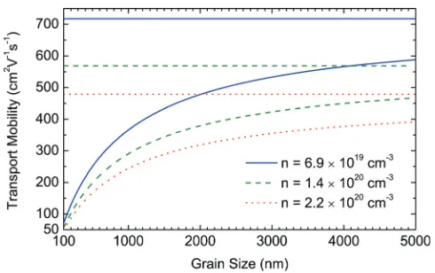
The variation of the transport mobility with grain size, predicted from the modeling, is represented in Fig.4for three different carrier concentrations. It is apparent that, as the grain size increases, the transport mobility tends to the bulk mobility within the grain. The mobility rises more steeply with increas-ing grain size when the grain size is low and closer to the bulk mean free path. So a large improvement of transport mobility is expected for a slight increase from the current grain size, with the rate of improvement diminishing as the grain size becomes much greater than the mean free path. This indicates that small improvements in the growth will have a relatively large effect on the mobility of CdO films.
Finally, it should be noted that for higher carrier concen-trations, the measured mobilities deviate somewhat from the model curves, as can be seen in Figs.2and3for optical and transport mobilities, respectively. As the formation energy of acceptors decreases and that of donors increases as the Fermi level increases toward the charge neutrality level,2the
den-sity of acceptors may no longer be negligible. Therefore, at high carrier densities, in addition to the ionized donors reducing the mobility, there may also be ionized acceptors acting as scattering centers. This partial compensation behavior, as previously observed for InN,24 would account for the deviation at high carrier density from the model curves in which only donors have been taken into account.
IV. CONCLUSIONS
The optical mobility of the CdO samples ranges from
209 to1116 cm2V1s1for carrier concentrations
rang-ing between 2:51020 and 2:61019cm3. Ionized impurity
scattering has been observed to be the dominant mechanism limiting the intra-grain mobility of CdO layers at room tem-perature. The transport mobilities ranging between20 and
124 cm2 V1 s1 are significantly lower than the optical
mobilities. As the bulk mean free path of the electrons is small compared to the film thickness, surface scattering is not a significant mobility reducing mechanism. Instead, scat-tering at grain boundaries is the prevailing mechanism reduc-ing the electron transport mobility. The commonly used models of grain boundary scattering for simulation of the transport mobility are not applicable to CdO as they assume a depletion layer at the grain boundaries. Given that CdO has a surface accumulation layer, which implies that electron accumulation is expected to take place at dislocations and grain boundaries, the effect of grain boundary scattering is simulated using alternative models. Simulation of the trans-port mobility shows that transtrans-port scattering takes place with
95% reflection of the electrons at the grain boundaries. Furthermore, the analysis of the transport mobility with respect to grain size in terms of the mean free path shows that, if the grain size of the CdO layers could be increased, electron transport would be significantly improved, leading to better conduction in transparent electrode applications.
ACKNOWLEDGMENTS
The Engineering and Physical Sciences Research Coun-cil, U.K., and the Spanish Government are acknowledged for FIG. 4. (Color online) Modeling of the transport mobility as a function of grain size for three CdO samples with different carrier concentrations and reflection coefficient,R¼0:95. Intra-grain mobilities for respective carrier concentrations are represented as horizontal lines.
[image:5.612.316.561.59.213.2]financial support under Grant No. EP/G004447/1 and Grant No. MAT2007-66129, respectively.
1F. P. Koffyberg,J. Sol. Stat. Chem.2, 176 (1970).
2D. T. Speaks, M. A. Mayer, K. M. Yu, S. S. Mao, E. E. Haller, and W.
Walukiewicz,J. Appl. Phys.107, 113706 (2010).
3
M. Yan, M. Lane, C. R. Kannewurf, and R. P. H. Chang,Appl. Phys. Lett. 78, 2342 (2001).
4S. Ghosh, A. Sarkar, S. Chaudhuri, and A. Pal,Thin Solid Films205, 64
(1991).
5
M. W. J. Prins, K.-O. Grosse-Holz, J. F. M. Cillessen, and L. F. Feiner, J. Appl. Phys.83, 888 (1998).
6D. H. Zhang and H. L. Ma,Appl. Phys. A62, 487 (1996). 7
J. Bruneaux, H. Cachet, M. Froment, and A. Messad,Thin Solid Films 197, 129 (1991).
8J. Y. W. Seto,J. Appl. Phys.46, 5247 (1975).
9P. D. C. King, T. D. Veal, P. H. Jefferson, J. Zu´n˜iga-Pe´rez, V.
Mun˜oz-Sanjose´, and C. F. McConville,Phys. Rev. B79, 035203 (2009).
10
K. Fuchs,Math. Proc. Cambridge Philos. Soc.34, 100 (1938).
11E. H. Sondheimer,Adv. Phys.50, 499 (2001).
12A. F. Mayadas and M. Shatzkes,Phys. Rev. B1, 1382 (1970). 13
D. K. Bowen and B. K. Tanner,High Resolution X-ray Diffractometry and Topography(Taylor and Francis, London, 1998).
14A. Pique´, R. C. Y. Auyeung, S. B. Qadri, H. Kim, B. L. Justus, and A. L.
Huston,Thin Solid Films377-378, 803 (2000).
15
J. Zu´n˜iga-Pe´rez, C. Munuera, C. Ocal, and V. Mun˜oz-Sanjose´,J. Cryst. Growth271, 223 (2004).
16C. C. Katsidis and D. I. Siapkas,Appl. Opt.41, 3978 (2002).
17M. Schubert, T. E. Tiwald, and C. M. Herzinger,Phys. Rev. B61, 8187
(2000).
18
H. Finkenrath, Physics of II-VI and I-VII Compounds, Semi-Magnetic Semiconductors, Landolt-Bo¨rnstein: Numerical Data and Functional Rela-tionships in Science and Technology. Group III: Crystal and Solid State Physics, edited by O. Madelung, M. Schulz, and H. Weiss, Vol. 17B (Springer, Berlin, 1982).
19S. G. Choi, J. Zu´n˜iga-Pe´rez, V. Mun˜oz-Sanjose´, A. G. Norman, C. L.
Perkins, and D. H. Levi,J. Vac. Sci. Technol. B28, 1120 (2010).
20
G. Yu, N. L. Rowell, and D. J. Lockwood, J. Vac. Sci. Technol. A22, 1110 (2004).
21E. O. Kane,J. Phys. Chem. Solids1, 249 (1957). 22
P. H. Jefferson, S. A. Hatfield, T. D. Veal, P. D. C. King, C. F. McConville, J. Zu´n˜iga-Pe´rez, and V. Mun˜oz-Sanjose´, Appl. Phys. Lett. 92, 022101 (2008).
23D. C. Look, H. Lu, W. J. Schaff, J. Jasinski, and Z. Liliental-Weber,Appl.
Phys. Lett.80, 258 (2002).
24