Overload Robust IGBT Design for SSCB Application
I. Supono
a, J. Urresti
a, A. Castellazzi
a, D. Flores
ba
Department of Electrical and Electronic Engineering, University of Nottingham, Nottingham NG7 2RD, UK
b
Instituto de Microelectrónica de Barcelona,Campus UAB. Cerdanyola del Vallès. Barcelona E-08193, Spain
Abstract
This paper presents an optimised power semiconductor architecture based on the CIGBT approach to be used in solid-state circuit breaker (SSCB) applications where the conduction losses have to be as low as possible without compromising the forward voltage blocking capability. Indeed, a high overcurrent turn-off and short-circuit withstand capabilities have to be ensured. Starting from a standard NPT-IGBT design for switching applications, the results show that the proposed device, which is optimised by the application of the individual clustered concept, offers a reduction in conduction losses of 13%, without compromise on voltage blocking capability. An original design solution is implemented to further ensure short-circuit and overload turn-off capabilities at maximum ambient temperature and twice the nominal rated current.
1. Introduction
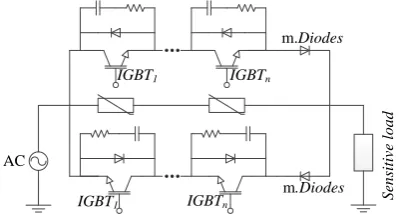
Fault detection and prompt removal is a critical enabler for the development of advanced electrical power transmission and distribution systems. Therefore, reliable circuit breakers as protection devices to prevent system damage and ensure reliability are essential. The performance and ratings of traditional electro-mechanical circuit breakers cannot meet the demands of upcoming distribution systems (e.g., Energy Internet [1]) (Figure 1). Hence, circuit breakers based on solid-state technology (SSCB) are a promising alternative, as they can bring along several advantages compared to traditional electro-mechanical solutions, such as improved voltage quality during short circuit and reduced short circuit current levels [2-5].
Presently, commercially available IGCTs are the best power devices for SSCB applications. However, SSCB oriented high voltage IGBTs [6-7] would be extremely attractive as they offer many advantages
(Table 1) such as reduced switching losses, simpler and more efficient gate driver, competitive price and mature process technology. Particularly for non-punch-through IGBTs the thermal stability is another attractive feature. This paper presents the design and optimisation of bespoke 3.3 kV IGBTs for SSCB applications, based on numerical 2D electro-thermal TCAD simulations and addresses fabrication aspects of optimised final architecture.
2. SSCB Bespoke Optimization
(Figure2), it is important that optimisation of the on-state performance does not degrade the blocking capability of the device which would require a higher number of series connected switches (eg. an 11kV network needs at least four 3.3kV IGBTs or seven 1.7kV IGBTs). Taking into account the SSCB requirements, the most important features when optimising a power semiconductor device are the maximum overload (current and temperature) turn-off capability, as well as the short circuit withstand capability. The robust handling capability against the two situations is essential for devices in SSCB because overload caused by excessive electric consumption and overcurrent caused by short circuit are fault conditions that likely occur in power transmission/distribution lines.
Table 1 Summary of benchmark performance comparison of the different power device
Feature IGBT GTO IGCT
Conduction
losses High Low Low
Switching losses Low High Medium
Failure mode Open/Short
circuit
Short circuit
Short circuit
Gate driver Simple,
compact
Complex, separated
Complex, Integrated Gate driver
power consumption
Low High Medium
Energy Storage
Transmission Distribution
Substation Transmission Controller
Distribution Controller
Substation
Electricity Provider
High power generations Distributed power generations Energy Storage
Industrial Commercial
Residential
End-user
Power line Communication line
Figure 1: Smart grid power distribution system
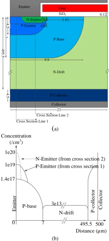
The IGBT optimisation starts from a selected reference device with an NPT-planar architecture (core cross-section plotted in Figure 3a), typically designed for switching applications and rated at 3.3kV-100A. The device high voltage drop
(indicated by 4.25V at 50 A/cm2) hints the possibility of device conduction losses improvement. The device is fabricated on a 500 µm thick wafer with a doping profile shown in Figure 3b. A new proposed structure is inspired by the clustered IGBT (CIGBT) concept, schematically illustrated in Figure 4, which is promoted in reducing conduction losses with a simple application of two additional deep diffusions [8-11]. Regarding these additional layers there are four optimization parameters: doping concentration and thickness of the two new layers.
IGBT1 IGBTn
IGBT1 IGBTn
m.Diodes
AC
S
en
si
ti
ve
l
o
a
d
m.Diodes
Figure 2: Schematic circuit of SSCB for ac based on IGBTs and diodes.
The doping profile of the proposed architecture is shown in Figure 4b including the tuning parameters. Two approaches have been considered, depending on the thickness of the P-base layer. The first case is based on a narrow P-base layer where the P-base junction (JP.base) is set at 2µm (opt-1 case),
while the second case (opt-2 case) is contemplates the use of the same P-body characteristics as those of the reference IGBT (7 µm junction depth). The optimisation of the four relevant parameters is divided into two groups, depending on the final target. The concentration and thickness of the additional P-layer (CAdd.P and tAdd.P) are optimised to
sustain the required breakdown voltage while the additional N-layer (CAdd.N and tAdd.N) is optimised to
get the minimum conduction losses. The starting point and the optimisation methodology are depicted in Figure 5.
[image:2.595.66.286.341.632.2]P-Emitter N-Emitter 23 4 .5 5.85 Emitter Gate SiO2 4.05
Cross Section Line 2 0.5
P-Base
N-Drift
P-Collector
Collector
Cross Section Line 1
4 .5 7 9.9 0.12 4 9 5 .5
(
a) Concentration(/cm3)
1e19 1.4e17 C o ll ec to r Distance (µm) E m it te r
7 495.5 500
0
3e13 P-base
N-drift P-c
o ll ec to r 1e20
P-Emitter (from cross section 1) N-Emitter (from cross section 2)
(b)
Figure 3: Reference 3.3 kV IGBT structure. Core cross-section (a) and doping profile (b).
The IGBT and the proposed structures are implemented and simulated with Silvaco™Atlas® [12]. Isothermal conditions are used for the steady-state analysis (on-steady-state vs. blocking voltage performance), while fully coupled mixedmode electrothermal simulations are performed for the transient analysis (turn-off and short-circuit capability). The self-heating effect model includes an estimated 4 cm2K/kW thermal resistance between the collector electrode (device backside) and the thermal ground (ambient temperature of 125°C).
N-Emitter LCell 4 .5 5.85 Emitter Gate SiO2 4.05
Cross Section Line 2 0.5
P-Base
N-Drift
P-Collector
Collector
Cross Section Line 1
J P .b as e 0.12 4 9 5 .5 J P .P lu s 9.9 tAdd.N tAdd.P
tAdd.N tAdd.P
(a) Concentration
(/cm3)
1e19 1.4e17 C o ll ec to r Distance (µm) E m it te r 495.5 500 0 Cadd.N Cadd.P 3e13 P + P-base
Add-N Add.P N-drift P-c
o ll ec to r 1e20
P-Emitter (from cross section 1) N-Emitter (from cross section 2)
JP.base t
Add.N tAdd.P
(
b)Figure 4: Optimized SSCB structure with schematic core cross-section (a) and parameterized doping profile (b).
N-layer Thickness (µm) N-layer Concentration (/cm3 ) 3 15e15 17e15
With P-layer concentration and thickness are constant
13e15
1 5
Starting variables
(
a)P-layer Thickness (µm) P-layer Concentration
(/cm3)
4 2.5e15
3.5e15
With N-layer concentration and thickness are constant
1.5e15
2 6
Starting variables
[image:3.595.321.522.116.493.2](
b)Figure 5: Optimization methodology.
[image:3.595.87.267.129.526.2] [image:3.595.318.523.542.672.2]The optimised additional P-layer for the opt-1 case corresponds to a maximum doping concentration (Cadd.N) of 3x1015cm-3 and a thickness
(tAdd.N) of 5 µm, leading to a forward blocking
capability of 3460 V. The simulated output characteristics revealed that the optimum additional N-layer has to be implemented with a maximum doping concentration (Cadd.P) of 1.58x1016 cm-3 and a
thickness (tAdd.P) of 3.8 µm in order to reach the
maximum improvement of the conduction losses (13% lower when compared to the reference IGBT losses of 60.26 W).
The simulated type-1 short-circuit test (Figure 6a) has corroborated that the proposed architecture withstands 10 µs short circuit at 1800 V input voltage. However the simulation of the overcurrent capability test encountered a latch-up event that makes the optimized structure failed to reach the targeted 100 A overcurrent capability. The overcurrent capability test is based on the double pulse circuit plotted in Figure 6b [13] with which the turn-on and turn-off processes at the nominal current (50 A) and the turn-off at overcurrent can be obtained.
2Ω
15V 1800V
7.2mH
A
C G
DUT
2Ω
15V
1800V A
C G
DUT
100nH
[image:4.595.317.511.116.417.2]a b
Figure 6: a. Switching test circuit; b. Short-circuit test circuit
[image:4.595.76.269.405.490.2]The simulated current density during the turn-off process of the proposed architecture are shown in
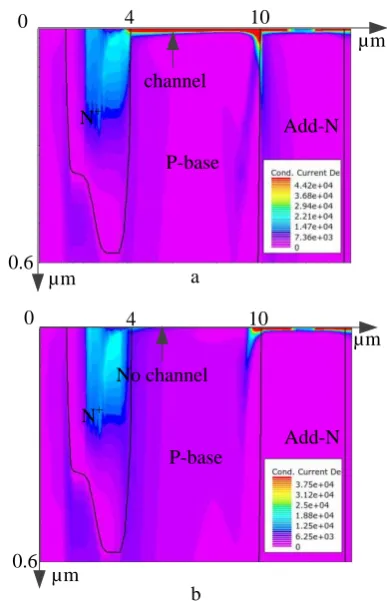
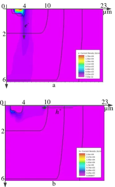
Figure 7, corroborating the latch-up of the parasitic N+/P-base/N/P thyristor. The conduction current density corresponding to 1 µs before turn-off clearly show the inversion channel on top of the P-base layer (Figure 7a). The inversion channel is completely removed 1 µs after the gate voltage is ramped to zero (Figure 7b). However, a high current density is still flowing through the structure due to the activation of the parasitic thyristor structure (Figure 7b). In this situation, electrons are injected from the narrow N+ layer into the P-base and holes are therefore injected from the additional P-layer into the additional N-layer, as shown in Figure 8.
µm
µm 10
0
µm
µm 10
0
0.6
channel
N+
P-base
Add-N
No channel
N+
P-base
Add-N a
b 4
4 0.6
Figure 7: Simulated conduction current density at (a) 1 µs before turn-off and (b) 1 µs after turn-off.
µm
0 23
2
6
e
-a
4 10
µm
0 23
2
6
h+
b
4 10
Figure 8: Simulated conduction current density at 1 µs after turn-off due to the latch-up event (a) electron concentration and (b) hole concentration.
The relevant electrical characteristics of the reference IGBT structure and the two cases of the proposed architecture are listed in Table 2.
In addition, as a first approximation, a fabrication process has been simulated (Silvaco™Athena®) in order to get an idea about its feasibility. From these simulations, we can conclude that the additional P and N wells (Figure 4b) can be achieved if high energy implantations (around 500 MeV) are performed and the later diffusions are carried out at 1200°C. Both implantations to form the P and N additional wells can be done within the same window implantation, therefore, just one additional mask level must be included.
[image:5.595.309.520.113.269.2]Figure 9: Turn-off performance of the two cases of the proposed architecture at normal conduction (50 A) and overcurrent (100 A) conditions.
Figure 10: Short-circuit performance of the two cases of the proposed architecture
Table 2: optimized structure performance comparison
Characteristics Reference Opt-1 Opt-2
Conduction loss (W) 60.26 52.48 50.89
Forward blocking (V) 3460 3460 3460
Overcurrent turn-off
capability x
10µs short circuit
capability
4. Conclusion
In conclusion, performed simulation results show that the additional N and P layers beneath the conventional P-base diffusion of an IGBT structure exhibit an improved on-state performance with no significant degradation of the forward blocking capability. Moreover, the improved maximum overload turn-off capability due to the thickened P-base diffusion is crucial to design a robust power
20.00 40.00 60.00 80.00 100.00 120.00 140.00
- 200 400 600 800
Co
n
d
u
ct
io
n
c
u
rr
en
t
(A
)
time (µs)
Opt-1
Opt-2
20 40 60 80 100 120 140 160 180 200
5 10 15 20 25
Co
ll
ec
to
r
cu
rr
en
t
(A
)
transient time (µs)
Opt-1
[image:5.595.87.273.118.420.2] [image:5.595.309.522.324.460.2]switch for SSCB applications. Hence, the proposed architecture is a promising candidate for high-performing SSCBs.
Reference
[1] Huang, Alex Q., et al. "The future renewable electric energy delivery and management (FREEDM) system: the energy internet." Proceedings of the IEEE 99.1 (2011): 133-148.
[2] Meyer, C., S. Schroder, and R.W. De Doncker, Solid-state circuit breakers and current limiters for medium-voltage systems having distributed power systems. Power Electronics, IEEE Transactions on, 2004. 19(5): p. 1333-1340.
[3] Vodyakho, O., et al. Design of a solid state fault isolation device for implementation in power electronics based distribution systems. in North American Power Symposium (NAPS), 2009. 2009. [4] Shammas, N.Y., The role of semiconductor devices in
high power circuit breaker applications. WSEAS TRANSACTIONS ON CIRCUITS AND SYSTEMS, 2005. 4(7): p. 826.
[5] Madan, M.K. and B.H. Chowdhury. Solid state fault interruption devices in medium voltage microgrid distribution systems with distributed energy resources. in Power and Energy Society General Meeting, 2012 IEEE. 2012. IEEE.
[6] Ming, C., et al. Development of topology and power electronic devices for solid-state circuit breakers. in Instrumentation and Measurement, Sensor Network and Automation (IMSNA), 2013 2nd International Symposium on. 2013.
[7] Chang, P., et al. Potential Use of Fault Current Limiter in VSC Based DC Transmission Systems. in Power and Energy Engineering Conference (APPEEC), 2012 Asia-Pacific. 2012.
[8] Sankara Narayanan, E.M., et al. A novel, clustered insulated gate bipolar transistor for high power applications. in Semiconductor Conference, 2000. CAS 2000 Proceedings. International. 2000. [9] Spulber, O., et al. 1.7kV NPT V-groove clustered
IGBT: fabrication and experimental demonstration. in Power Semiconductor Devices and ICs, 2003. Proceedings. ISPSD '03. 2003 IEEE 15th International Symposium on. 2003.
[10] Sweet, M., et al. Experimental Demonstration of 3.3kV Planar CIGBT In NPT Technology. in Power Semiconductor Devices and IC's, 2008. ISPSD '08. 20th International Symposium on. 2008.
[11] Sweet, M., et al., Clustered insulated gate bipolar transistor: a new power semiconductor device. Circuits, Devices and Systems, IEE Proceedings -, 2001. 148(2): p. 75-78.
[12]Silvaco Inc., “Atlas User’s Manual”, 2012 [13] BRITISH STANDARDS INSTITUTION.
Semiconductor devices — Discrete devices — Part 9: Insulated-gate bipolar transistors (IGBTs). London: