Fast Functional Modelling of Diode-Bridge
Rectifier Using Dynamic Phasors
T. Yang
,
S. V. Bozhko
,
G. M. Asher
The University of Nottingham, Nottingham NG7 2RD, UK
This paper is a postprint of a paper submitted to and accepted for publication in IET Power Electronics
and is subject to Institution of Engineering and Technology Copyright. The copy of record is available
at IET Digital Library
Corresponding Author: Dr Tao Yang
Power Electronics, Machine and Control Group Faculty of Engineering
The University of Nottingham Nottingham NG7 2RD United Kingdom
Phone: +44 (0)115 748 4739
Email [email protected]
Abstract— In this paper, a functional model for diode-bridge rectifiers is developed based on the dynamic phasor concept. The
developed model is suitable for accelerated simulation studies of the electric power systems under normal, unbalanced and line
faulty conditions. The high accuracy and efficiency of the developed model have been demonstrated by comparison against
three-phase time-domain model and against the model employing synchronous space-vector representations. The experimental
verification of the developed model is also reported. In addition, an error analysis shows that the error of the developed model is
less than 10% at the most severe unbalanced conditions. The prime purpose of the model is for the simulation studies of
more-electric aircraft power architectures at a system level; however it can be directly applied for simulation study of any other
electrical power system interfacing with uncontrolled diode bridge rectifiers.
I. INTRODUCTION
There has been seen a significant penetration of power electronics into electric power systems (EPS) in recent years.
For example, terrestrial EPS’s particularly at distribution level, promise a multiplicity of power electronic converters to
handle renewable sources, energy storage or EPS conditioning. A similar scenario pertains for isolated and mobile EPS, such
as more-electric aircraft (MEA) and more-electric ship. In the MEA the electric power conversion is required to manage
power distribution, landing gear, flight actuation and other functions [1].
The use of large numbers of power electronic devices brings significant modelling challenge at the EPS system
level due to the system complexity and the wide variation in time constants. The challenge is to balance the simulation speed
against the model accuracy and this is dependent on the modelling task. Four different modelling layers are defined
according to the modelling bandwidths i.e. architectural models, functional models, behavioural models and component
models [2], [3]. The architectural layer computes steady state power flow and is used for weight, cost and cabling studies. In
the functional level, the system components are modelled to handle the main system dynamics up to 150Hz and the error
should be less than 5% in respect of the behaviour model accuracy. The behavioural model uses lumped-parameter
subsystem models and the modelling frequencies can be up to hundreds of kHz. The component models cover high
frequencies, electromagnetic field and electromagnetic compatibility (EMC) behaviour, and perhaps thermal and mechanical
stressing. The bandwidth of component models can be up to in MHz region if required.
Targeting for acceptable simulation times for system-level EPS modelling, a number of approaches have been
investigated. Average state-space models [4] are a standard technique for considering only the fundamental wave converter
behaviour. Average modelling of ac distribution systems involves transforming the three-phase ac signals to a synchronous
rotating dq frame, henceforth termed the dq0 model. This method has been used in modelling MEA electric power systems
and is proved to be an effective technique [3]. A model with three-phase ac variables is henceforth called an abc model.
One of the disadvantages of the dq0 approach is that under faulty and unbalanced conditions double-frequency
components appear and the simulation time steps must be drastically reduced to maintain accuracy. An alternative approach
that can address this problem is dynamic phasors (DPs) [5, 6]. The DP method has been applied to the modelling of terrestrial
EPS systems including imbalanced regimes [7, 8]. Comparative study of a simple EPS with line faults carried out in abc, dq0
and DP domain is given in [9] where the efficiency of the DP approach is demonstrated. The DP method has also been
applied for modelling of electrical machines [10, 11] and flexible ac transmission systems [12], including active filters [13]
and static synchronous compensator (STATCOM) [14]. In [15] and [16], a DP model for thyristor-based high-voltage direct
Different models for uncontrolled diode-bridge rectifiers (DBs) have been developed in recent publications. A
comprehensive analytical model is developed in [17] and [18], where different operation modes of DBs have been thoroughly
studied. Another mathematical model for analysing DBs based on switching functions is introduced in [19]. An average
model for DB is proposed in [20]. However, all these models are only for steady-state applications and the power supply is
assumed to be balanced. This paper aims to develop a DP model for DBs. This model can be used for both steady-state and
transient studies, under balanced and unbalanced conditions. At the time of this study development, no report on DB
modelling in DP domain has been published. The most similar to DBs modelled using DP approach is a thyristor-based
HVDC converter [16]. In addition, the model reported in [16] is suitable only for balanced operations. The DB functional
model presented in this paper is based on the DB relations between ac and dc terminal variables. The negative sequence
under unbalanced or fault conditions is treated as a disturbance in the model. Both the 2nd and 6th harmonic on the dc-link voltage are conveniently included in the reported DP model. This enables to cover the ac imbalanced voltage and dc ripple
voltage for both continuous and discontinuous operation.
The main results of the paper are summarised as follows:
- The DP approach has been successfully applied to develop model an uncontrolled DB rectifier applicable for
accelerated simulation studies of complex EPS, both balanced and unbalanced, and is consistent with the functional
modelling layer specifications in [3]. The model is independent on other EPS devices and may be used as a library element
interfacing within an extended three-phase EPS models
- The model is verified experimentally under both balanced and unbalanced operation
- The computational effectiveness of the developed model is proved through comparison against time-domain abc
switching and functional non-switching dq0 models and a significant computational acceleration is demonstrated.
II. DYNAMICPHASORS
This Section, in order to keep the paper self-containment and to assist readability, shortly revises the basic concepts
that are employed for the development of the diode bridge model in DP domain. For the readers who are not familiar with the
concept, it is recommended to refer to the basic DP theory [5] since it will be intensively used throughout the rest of the
paper.
The DP concept assumes that a time-domain nearly-periodic waveform x(τ) can be represented on the interval τ(t
] , ( , ) ( )
( X t e t T t
x
k
jk
k s
(1)
where ωs=2π/T and T the fundamental period of the waveform. Xk(t) is the kth Fourier coefficient in complex form referred to
as a “dynamic phasor” and determined as follows:
k t
T t
jk
k x e d x
T t
X
s
) ( 1 )
( (2)
where k is the DP index and angular brackets are used to denote DP-domain variables. In contrast to the traditional Fourier
Transformation (FT), these Fourier coefficients are time-varying as the integration interval (window) slides through time. As
it follows, the DP represents the variation in specific frequency component over time. The required accuracy of the
time-domain variable approximation can be achieved by appropriate selection of a DP set K for a particular modelling task. For
example, for dc-like variables and signals the index set only includes the component k=0, and for purely sinusoidal ones k=1.
A key factor in developing dynamic models based on DP is the relation between the derivatives of the variable x(τ)
and the derivatives of kth Fourier coefficients [5]:
) ( )
(
t X jk dt
t dX dt dx
k s k
k
(3)
This can be verified using (1), (2), and may be used in evaluating the kth phasor of time-domain model. Another
important property of DP is that the kth phasor of a product of two time-domain variables can be obtained via the convolution
of corresponding DPs:
i k i i
k x y
xy
(4)
The properties (3) and (4) play a key role when transforming the time-domain models into DP domain. Algebraic
manipulations in this paper will also exploit the following property of real functions x(τ):
) ( )
(t X* t
Xk k (5)
where the notation * denotes a complex conjugate.
III. UNCONTROLLED DIODE-BRIDGE RECTIFIER
A key objective of this paper is development of a computationally efficient model that can represent the DB
require consideration of switching behaviour [3]. Hence, our study is based on the non-switching model that is reviewed in
this Section.
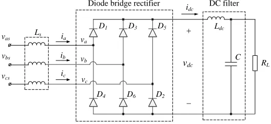
A three-phase diode bridge rectifier is well-documented ac/dc converter and it is shown in Fig.1. In general case, it
is supplemented by an output dc filter LdcC and a front-end inductance Ls representing feeding cables, ac chokes etc. The dc
load is shown as an equivalent resistance RL. This converter employs uncontrolled diodes; hence the switching instants are
determined by the circuit condition exclusively. The time-domain non-switching DB model under balanced conditions is well
developed and documented in many publications, for example [17, 21].
C Ldc
D1 D3 D5
D4 D6 D2
RL vdc idc vas vbs
vcs ic
ia ib va vb vc Ls
[image:6.612.175.439.220.341.2]Diode bridge rectifier DC filter
Fig. 1 Three-phase diode bridge rectifier
Under the symmetrical balanced supply the rectifier terminal voltages can be represented as
) 3 / 2 cos( ) 3 / 2 cos( ) cos(
t t t v v v v m c b a abc V (6)where vm is the voltage magnitude, ω is the supply electrical frequency and φ is the initial phase angle. The fundamental of
diodes switching function then is given as follows [22]:
) 3 / 2 cos( ) 3 / 2 cos( ) cos( 3 2
t t t S S S c b a abc S (7)The switching function (7) defines the input-output relations for the diode bridge:
m abc T abc dc v v
3 3 S V (8)
dc abc
abc S i
I (9)
where Iabc=[ia ib ic]T- an input ac current in vector-matrix form, vdc and idc – rectifier output dc voltage and current. As it
dc
m i
i
3 2 (10)
In a presence of front-end inductance Ls the dc-link voltage (8) reduces due to the commutation effect [22]. Normally, this
effect is taken into account by introducing in (8) an additional term corresponding to a voltage drop across the resistance of rf
value:
s
f fL
r 6 (11)
In the following paper sections we will also intensively use the voltage (6) expressed as a space vector:
2 /3 2 /3
3
2 va vbej vce j
v (12)
It is convenient to analyse three-phase power electronic circuits in synchronously rotating frame[3], [4]. Define the dq frame
such that it rotates with the grid electrical frequency ω. Any three-phase variable fabc can be expressed in the dq frame such
that:
abc
dq
Tf
f
(13)where T is a transformation matrix:
)
3
2
sin(
)
3
2
sin(
sin
)
3
2
cos(
)
3
2
cos(
cos
3
2
t
t
t
t
t
t
T
(14)Combining (8)-(10), (12)- (14) yields the following:
2 2
3 3
q d
dc v v
v
(15a)dc q
d
m i i i
i
3 22
2
(15b)
where vd and vq are d and q components of voltage vector (12). Since the input current fundamental is in phase with the input
voltage, its d and q components are as follows:
; sincos q m
m
d i i i
i (16)
Under the balanced supply, φ is equal to the initial phase of the input voltage and can be derived from voltage d- and
q-components:
vq vd
1
tan
(17)
the output dc voltage/current. These equations will be employed for the development of DB model in the DPs domain.
IV. DYNAMIC PHASOR DBMODEL DEVELOPMENT
In this Section the non-switching DP-domain DB model is developed. We will start with establishing how to map
the generally unbalanced supply voltage vector (12) expressed in terms of synchronous dq frame from time domain into the
frequency domain of DPs and how the corresponding DPs can be derived from time-domain values of individual phase
voltages va, vb, vc for both balanced and unbalanced conditions. Then the DB input-output relations (15) will be transformed
into DPs and the DP-domain DB model will be assembled using the derived relations.
A. Input voltages and current in dynamic phasors domain
In general cases, the DB terminal voltage can be represented by:
)
cos( i
i
i V t
v
, i=a,b,c (18)where Va, Vb and Vc are phase voltage magnitudes, and φa, φb, φc – their phase angles. Applying the Euler formulae, each of
these components can be rewritten as:
c b a i e e V e e V v t j j i t j j i i i i , , , 2
(19)
The DPs of phase voltages can be derived applying the definition (2) and selecting the DPs set as k=1 since (18) includes
only the fundamental component:
c b a i e V v v e V
v i j i
i i
i j i
i , , ,
2 1 , 2 1 * 1 1
1
(20)
Combining equations (12), (18), (19) and re-arranging the terms results in the following relation:
* 2 /3
1 3 / 2 * 1 * 1 3 / 2 1 3 / 2 1 1 3 2 3
2 j
c j b a t j j c j b a t
j v v e v e e v v e v e
e
v (21)
It is clearly seen that the two right-hand side terms define the positive and the negative sequences of input voltage vector.
The latter will appear under unbalanced phase voltages only. In terms of synchronous dq frame defined by (14), the voltage
vector (21) can be derived as:
* 2 /3
1 3 / 2 * 1 * 1 2 3 / 2 1 3 / 2 1 1 3 2 3
2
j c j b a t j j c j b a t j q
d jv ve v v e v e e v v e v e
v (22)
j t q d q d qd
jv
V
jV
V
jV
e
v
0
0
2
2 2 (23)where variables Vd0, Vq0, Vd2 and Vq2 can be calculated as:
2 /3
1 3 / 2 1 1 0 Re 3
2 j
c j
b a
d v v e v e
V
(24a)
2 /3
1 3 / 2 1 1 0 Im 3
2 j
c j
b a
q v v e v e
V
(24b)
* 2 /3
1 3 / 2 * 1 * 1 2 Re 3
2 j
c j
b a
d v v e v e
V
(24c)
* 2 /3
1 3 / 2 * 1 * 1 2 Im 3
2 j
c j
b a
q v v e v e
V
(24d)
The d- and q- axes components of the input voltage vector vd and vq can be derived from (23) by separation of real and
imaginary parts:
t
V
t
V
V
v
t
V
t
V
V
v
d q q q q d d d
2
sin
2
cos
2
sin
2
cos
2 2 0 2 2 0
(25)The following important conclusions should be made analysing the result given by (25):
under balanced conditions the voltage dq-components become dc-like: vd=Vd0 and vq=Vq0;
if the supply voltage is unbalanced, the dq frame components of the voltage vector will also include the second
harmonics;
the DP set K, in order to represent the supply voltage in dq frame under both balanced and unbalanced conditions,
should include zero and 2nd harmonics, i.e.
0,2
K (26)
The mapping of vd and vq into DPs is established in Table I. The current id and iq can be derived in the same manner.
TABLE I.DYNAMIC PHASORS FOR DB INPUT VOLTAGE AND CURRENT IN SYNCHRONOUSLY ROTATING FRAME
Variable Dynamic phasors
k=0 k=2
v
dv
qi
di
q 0 0 d d Vv vd 2(Vd2jVq2)/2
0 0 q
q V
v vq 2(Vq2jVd2)/2 0
0 d
d I
i id 2(Id2jIq2)/2
0 0 q
q I
B. DC-link Voltage in dynamic phasors domain
In this Section we will transform the DB voltage input-output relation (15a) into the DP domain. The main
challenge is due to a non-linear nature of this equation that makes the direct application of DP definition (2) non-analytic.
The approach we propose in this paper expands (15a) into a Taylor series with respect to vd and vq followed by the
transformation of the truncated series into the DP domain. Considering the DB output voltage as a function of two variables
vd and vq as follows:
2 2 ,
1
3
3
)
(
v
dv
qv
dcv
dv
qf
(27)Approximating (27) by the Taylor series requires selection of the operation point. The natural choice is the pair {vd,
vq} under balanced conditions. Hence, the operating point is defined as {Vd0, Vq0} according to (25). The Taylor expansion of
(27):
(
)(
)
!
2
)
(
!
2
)
(
!
2
)
(
!
1
)
(
!
1
0 05 2 0 4
2 0 3
0 2
0 1
0 d d q q d d q q d d q q
dc
v
V
v
V
k
V
v
k
V
v
k
V
v
k
V
v
k
k
v
(28)where ki are constants depending on the selected operation point. These can be calculated using (24), (27) and are given in
Appendix I.
The series (28) can be converted into the frequency domain after suitable truncation. Since vd and vq include
harmonics up to the second order in our model, we truncate 3rd-order and higher terms in (28). From (28), in the balanced condition (vd=Vd0 and vq=Vq0) the dc-voltage vdc will be constant and equal to k0 which is associated with the input voltage
positive sequence. Under unbalanced conditions, the negative sequence will appear and disturb the diodes switching function
(7). The impact of the negative sequence can be represented as a disturbance to vdc (27) in a form of the second harmonic
appearing according to (25) in both vd and vq. Applying the DP index set (26) and employing the convolution property (4) to
the truncated Taylor series of (28), the DPs of dc-link voltage vdc are derived as follows:
* 2
2 *
2 2 5 *
2 2 4 *
2 2 3 0
0 d d q q d q d q
dc
k
k
v
v
k
v
v
k
v
v
v
v
v
(29a)2 2 2 1
2 d q
dc
k
v
k
v
v
(29b)The DPs 〈vd〉0, 〈vd〉2,〈vq〉0 and〈vq〉2are given in the Table I in a previous Section. Hence, the DPs for dc-link
C. Accounting for the dc-voltage ripple
The converter output voltage calculated using (29) exhibits only dc-component under balanced conditions and
includes the 2nd harmonic under unbalances. For functional-level simulation studies this may be sufficient. However, there is a room for convenient model improvement by inclusion into a model the 6th harmonic on the dc side voltage that exhibits under balanced conditions in the rectifier under consideration [22]. This section demonstrates how this component can be
introduced into the DP-based model if required.
Under the balanced operation, the 6th harmonic in the dc voltage is due to the 5th and 7th harmonic in the switching function [23] that can be given as:
) 7 7 cos( 7 3 2 ) 5 5 cos( 5 3 2 7 ,
5
t
t
Sa (30a)
) 3 2 7 7 cos( 7 3 2 ) 3 2 5 5 cos( 5 3 2 7 , 5
t t
Sb (30b)
) 3 2 7 7 cos( 7 3 2 ) 3 2 5 5 cos( 5 3 2 7 , 5
t t
Sc (30c)
Combining (30) with (8), (9) and (12), the magnitude of the 6th harmonic in dc voltage vdc6 and its phase angle φdc6 are derived as follows:
2 0 2 0 2 0 2 0 6 7 3 3 5 3 3 q d q d
dc V V V V
v
(31)
0 0
1 6
6
tan
q/
ddc
V
V
(32)In a way similar to (20), one can derive the corresponding DP:
6 6 6 2 1 dc j dc
dc v e
v (33)
This extra DP can be added to the previously derived set (29) to represent the DB dc-link voltage in the DP domain.
The time-domain value of dc-link voltage can be calculated using the definition (1):
e
v
k
t
m
v
k
t
e
t
v
t
v
dc k dc kk
t jk k dc
dc
sin
cos
2
)
(
)
(
(34)D. Rectifier ac currents
The linear relationship between the magnitude of the current vector im and the dc-link current idc was given in (15b)
and can be transformed into DP domain as follows:
k dc k
m i
i
3 2
(35)
The ac input currents of the rectifier are dependent on the dc load current which is determined jointly by the dc-link
voltage vdc and by the load itself. In the proposed model the dc current is derived from its time-domain value measured at the
model output and then converted into the DP. The DP index for 〈idc〉k for linear loads should be chosen according to 〈vdc〉k,
i.e. k={0,2,6}. However, using the following equation
dc
dc
i
i
0 (36)
allows us to avoid calculating of idc2 and idc6 with the DP definition (1) and thus no cumbersome calculation of ∫ xe-jkωtdt
t
t-T
is needed. With (36) all the dc-link current information will be included in idc0. The fluctuation of idcwill be reflected to the fundamental DPs ia,b,c1 through idc0 and this will be illustrated later in the paper. From (35), the same DP set k=0 will
apply to im. The DP for the input current d- and q-axis components can be derived using (16) as follows:
i k k
i i m k
q
i k k
i i m k
d
i i
i i
sin cos
0
0 (37)
The main challenge in calculation of (37) deals with the establishing the DPs for non-linear functions sinφ and cosφ.
As in previous Section, the approximation is executed by a Taylor series. The non-linear terms are expressed via d- and
q-axes voltagecomponents:
2 2 2
(
,
)
cos
q d
d q
d
v
v
v
v
v
f
(38a)2 2
3( , )
sin
q d
q q
d
v v
v v
v f
(38b)Selecting the operation point {Vd0, Vq0}, using the same technique as that dealing vdc in (27) derives,
2 * 2 *
2 2 5 *
2 2 4 * 2 2 3 0 0
2 2 2 1 2
cos h vd h vq (40b)
2 * 2 * 2 2 5 * 2 2 4 * 2 2 3 0 0
sin
g g vd vd g vq vq g vd vq vd vq (40c)2 2 2 1 2
sin
g vd g vq (40d)where hi and gi are constant coefficients that depends on a selected operation point and given in Appendix I. Hence, the DPs
for the non-linear functions (38) are derived. Then, the DPs for DB input current d- and q-components can be easily derived
using (37). Finally, if the modelling task instead of d- and q- current components requires the current in a form of three-phase
ac variables, then the DPs (37) have to be transformed into abc frame as described in the following Section.
E. DQ0 to ABC transformation in dynamic phasors domain
Applying the convolution property to the abc/dq transform given by (13) and (14) yields:
2 2 * 1 1 0 0 1 1 1 1 1 q d q d c b ai
i
i
i
i
i
i
T
T
(41)where, T-1 is the generalized inverse matrix T:
)
3
2
sin(
),
3
2
cos(
)
3
2
sin(
),
3
2
cos(
sin
,
cos
1
t
t
t
t
t
t
T
(42)Calculation of 〈T-1〉1 requires the DPs for cosωt and sinωt. As ω is constant, the DP index for these will include the only
component k=1, hence employing (2) one can easily derive:
4
3
4
1
4
3
4
1
4
3
4
1
4
3
4
1
5
.
0
5
.
0
1 1
j
j
j
j
j
T
(43)Using (43), the DP of input currents in abc frame can be derived easily. Furthermore, applying definition (1), the
corresponding time-domain current values can be calculated as well.
F. Model assembling
The equations derived in the sections above can be combined together in order to build the DP-domain model of the
(36)
(34)
va
vb
vc
C
ib
ic
ia
V
V
V
1
a
v
1
b
v
1
c
v
0
dc i
0,2,6
dc v
+
_
ω
b c a
Transform (24) and Table I
0,2
d v
0,2
q
v
0,2
d
i
0,2
q
i
Voltage Relation (29), (33) and
Table I Current Relation
(37), (40) and Table I dq/abc
Transform (41)
1
a i
1
b i
1
c i
Transform Eqn.(1)
DP calculator
Eqn. (2)
vdc
idc
idc
+
_
Fig. 2 DP model of the DB rectifier
The current flow shown in Fig.2 illustrates the mapping of idc into the AC currents ‹ia,b,c›1. With (36), all the
information in idcis reserved in the DP ‹idc›0. This makes ‹ia,b,c›1 a function of the time-varying current idc and allows the
harmonic characteristics in the ac currents to be represented by the fundamental DPs ‹ia,b,c›1. The DP model shown in Fig. 2
can be used in EPS simulations with no need for the user to understand DP theory. In case studies when the DB rectifier is
fed through an inductive line, a small capacitor should be added at input terminals to avoid model state redundancy and
related numerical problems. For the user who wishes to build the entire EPS model in the DP domain, the model does not
need the interface blocks (coloured in grey in Fig.2) since the DP variables are already available and the DB model can be
directly interfaced to the other EPS model blocks.
V. MODEL ERROR ANALYSIS
In the diode-bridge DP-domain model derived in previous Sections we employed linearization of (27) and (38)
around the operation point determined by the voltage positive sequence; the negative sequence was treated as a disturbance.
With the increase of the negative sequence this consideration may result in some modelling error that is a subject of analysis
in the current paper Section.
Consider the modelling error defined as:
% 100
_ _ _
T BM dc
T
DPM dc T
BM dc
dt v
dt v
dt v
(44)where vdc_BM is the dc-link voltage calculated by the benchmark model (this is a full switching model in three-phase
mode case described in the previous Section with the set of phase voltages as:
)
3
/
2
cos(
80
),
sin(
),
cos(
80
t
v
V
t
v
t
v
a b b b c (45)Evaluation of the error (44) has been performed by series of simulations varying the magnitude of phase b voltage
Vb from 0 to 120V and its phase b from 0 to 2π. Thus all balanced and unbalanced conditions are covered. The results of the
error analysis are depicted in Fig. 3 as a function of Vb, b and the unbalance factor λ. The latter is defined as the ratio of between the magnitudes of negative-sequence voltage vn and the positive-sequence one vp and written as:
v
n/
v
p (46)
Fig. 3. Analysis of the DP model: (a) - 3D presentation of =(Vb,b), λ= λ(Vb,b); (b) – 2D graph showing =(b, λ) with Vb=120V
It is clearly seen that the model error greatly depends on unbalance factor λ. This is reasonable since with the
increase of λ the disturbance from the negative sequence becomes more severe and thus the operation point shifts from {Vd0,
Vq0} as selected for linearization of (27) and (38). The modelling error has a maximum when b=5π/6 and Vb=120V – at these
values λ takes an extreme value. In practice, if the negative sequence becomes dominant, i.e. λ>1, the operation point should
be selected using the negative sequence {Vd2, Vq2} considering the positive sequence as a disturbance. Thus, the model can be
conveniently adopted for this case. Hence in the error analysis we only have to consider the cases when λ[0,1] (below the
horizontal line λ=1 in Fig. 3(b)) . For the case of balanced operation λ=0 the modelling error is less than 2%. The line-to-line
fault can be considered as the case when λ=1 and Vb=120V; the modelling error for this event is less than 10% as follows
from Fig. 3(b). For the case of phase-to-ground fault (Vb=0V) the modelling error is very small and is always less than 2%.
The modelling accuracy analysis confirms that the developed DP model is well suitable for the functional modelling
of uncontrolled diode-bridge rectifier. The accuracy of the DP model will be experimentally validated and discussed in the
0 2pi/3 4pi/3 2pi
0 1 2 3 4 5
b (rad)
0 2pi/3 4pi/3 2pi0
20% 40% 60% 80% 100%
following section.
VI. MODELEXPERIMENTALVALIDATION
A test rig shown in Fig.4 with parameters given in Appendix III has been employed for the model verification. A
programmable source Chroma II has been used to apply balanced and unbalanced voltages to the DB. The model has also
been verified in continuous and discontinuous current modes as reported below. In the simulation model, small capacitors
(C=1e-8F) were added between the diode bridge and the line inductors as suggested in Section IV.F above.
+
D1 D3 D5
D4 D6 D2
RL vas
vbs
vcs ic
ia ib
va vb vc Rs Ls
C LDC
vdc idc
CHROMA II Programmable
power supply
[image:16.612.147.465.243.357.2]R’L Sw1
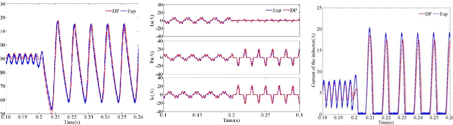
Fig.4. The experimental rig A. Continuous mode
In the experiment, the initial value of balanced supply voltage was set to values va=vb=vc=40V/50Hz to avoid
source protection triggering when imitating the fault. The phase A voltage is set to zero at t=0.2s in order to perform the
line-to-ground fault to the system. A continuous current mode is ensured with a heavy load on dc-link side by switching on Sw1
and paralleling RL and R’L ’
). The simulation and experiment values of dc-link voltage, input currents and the inductor current
are compared in Fig. 5.
Fig. 5. The dc-link voltage (a), input current (b) and inductor current (c) in continuous mode with phase A loss at t=0.2s
[image:16.612.84.540.541.667.2]harmonic included in the DP model, the results from the experiment and DP model are well matched. After the
line-to-ground fault, the dc-link voltage fluctuates at double frequency. In this case, the 2nd harmonic is included in the DP model and the results from the experiment and simulation are well matched. The DP model and experiment results for ia,b,c are
shown in Fig. 5(b) and they are well matched before and after the fault occurs. The DC-link current idc is shown in Fig. 5(c)
and it changes from a continuous current mode (CCM) to a discontinuous mode (DCM) when the fault occurs. It can be seen
that under CCM and DCM conditions, the DP model demonstrates good performance in both cases.
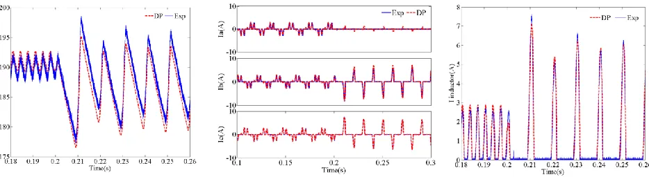
B. Discontinuous mode
In this case the switch Sw1 is open hence a large load resistance RL results in a small dc-link current which makes
the inductor current discontinuous. The experiment starts with balanced voltages set va=vb=vc=80V/50Hz followed the loss
of phase A supply (va=0) at t=0.2s. The simulation and experiment values of dc-link voltage, input currents and the inductor
[image:17.612.78.545.341.469.2]current are compared in Fig. 6.
Fig. 6 The dc-link voltage (a), input current (b) and inductor current (c) in discontinuous mode with phase A loss at t=0.2s
As can be seen in Fig. 6(a), vdc has a 6
th
harmonic under the balanced condition and a 2nd harmonic under the line fault condition. In both cases, the results from the DP model are well matched with experiment. The ac side currents from the
experiment and the DP model, shown in Fig. 6(b), are well matched before and after the fault occur. The dc-link current idc,
shown in Fig. 6(c), indicates that the rectifier works under the DCM under both normal and faulty conditions. The results
from the experiment and DP model are well matched in both cases.
Following the results in this section, the proposed model successfully verified under balanced and unbalanced
VII. COMPUTATIONTIMESTUDIES
Since the accuracy of the DP model has been validated, this section will focus on the assessment of the
computational performance of the developed DP model. For this purpose, different modelling techniques have been applied
to an example EPS given in Fig.7 and the CPU time taken for simulation run has been compared. The simulated scenario
includes balanced and unbalanced operation, as well as continuous and discontinuous DB modes as detailed below. The
system parameters are given in the Appendix III.
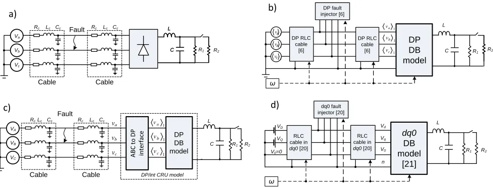
Fault
Lc
Cable Cable
Va
Vb
Vc
Cc
Rc Rc Lc Cc
a)
C L
C L
R1 R2
DP DB model
DP RLC cable [6]
DP fault injector [6]
DP RLC cable [6]
1
A
v
1 B
v
1 C
v
1
a
v
1
b
v
1
c
v b)
ω
C L
R2
R1
c)
Lc
DP DB model
Cable Cable
VA
VB
VC
Cc
Rc Rc Lc Cc
A
B
C
t
o
D
P
in
te
rf
ac
e
va
vb
vc
-DP/int CRU model
1
a
v
1
b
v
1
c
v
C L
Fault
R2
R1
dq0
DB model
[21]
VD
VQ
V0=0
dq0 fault injector [20]
d)
ω
Vd
Vq
V0
n
C L
R2
R1 RLC
cable in dq0 [20]
[image:18.612.62.552.195.382.2]RLC cable in dq0 [20]
Fig. 7 EPS models for comparison: (a) abc model; (b) DP model; (c) DP/int model; (d) dq0 model.
The following EPS models have been developed and compared:
- A three-phase EPS with a switching DB rectifier model (ideal switches) illustrated by Fig.7(a) and referred to as
an abc model;
- An EPS with all the elements are DP models as shown in Fig.7(b). There are no three-phase time-domain
variables in this model and it is referred to as DP model;
- An EPS in which only the DB is modelled using DPs with three-phase interfaces as shown in Fig.7(c). The EPS
is seen by the user as a three-phase system and the DP formulations are not visible. This is termed the DP/int model;
- An EPS with all the elements in dq0 frame [24, 25] as shown in Fig.7(d).
A. Models comparison under balanced operation
The simulation scenario in this case assumes the DB operation in discontinuous model followed by impact of dc
load making the dc-link current continuous at t=0.1s. The dc-link voltage and current for all the models are shown in
mode. In contrast, the dq0 model delivers correct average vdc and idc values of vdc only in continuous mode, however in
discontinuous mode it demonstrates a significant discrepancy compare to models. This is because in discontinuous mode
when idc becomes zero the capacitor discharges to the load impacting the average value of vdc, however the dq0 model does
not include the effect of additional charging received due to the 6th harmonic.
The CPU time taken by different models is compared in Table II. The DP and DP/int models in balanced operation
are more than 20 times faster than abc model, however the dq0 model is much faster. The cumulative CPU time during the
simulation is shown in Fig.8(b). Note that when the continuous mode occurs the abc model slows down dramatically but DP
and DP/int models maintain the simulation speed. This is because in discontinuous operation there are no commutating
periods in DB and only two diodes conduct at any instant, however in continuous mode there are commutation periods
requiring from the solver reduction of integration time-steps thus slowing down the simulation.
(a) (b)
[image:19.612.117.525.298.647.2](c) (d)
TABLE II.CPU TIME TAKEN FOR BALANCED SCENARIO SIMULATION
Model: abc dq0 DP DP/int
CPU time taken: 49.17 0.206 2.079 2.369
Performance index: 1 238 24 21
Summarizing, in balanced conditions the DP and DP/int models are slower than dq0 model due to complexity and
inclusion of higher harmonics, however the dq0 model is much less accurate especially in discontinuous mode.
B. Line-to-line fault
The unbalanced regime is simulated as a line-to-line fault (phases A and B are shortened via the fault resistor
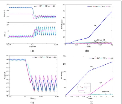
Rfault=1e-4Ω) at t=0.4s. The switch Sw1 is “on” to ensure the continuous mode prior the fault. The dc-link voltage is shown in
Fig.8(c). As one can conclude, the DP and DP/int models match well to abc model under both balanced and unbalanced
regimes. The dq0 model in the balanced condition (t<0.4s) reflects the voltage average value.
The CPU time taken by different models is compared Table III. As one can conclude, the efficiency of the dq0
model is lost in unbalanced operation. This is clearly seen from the cumulative CPU time graph in Fig.8(d): the slope
corresponding to dq0 model is the largest when t>0.4s. In contrast, the DP-based models maintain their simulation speed and
for the entire scenario they are 40 times faster of compare to the abc model and 20 times faster than the dq0 model.
Table III. CPU time taken for unbalanced scenario simulation
Model: abc dq0 DP DP/int
CPU time taken: 214.4 111.4 5.405 5.448
Performance index: 1 2 40 40
Hence, the results above have confirmed a very good efficiency of the developed DB model compare to other
modelling techniques, in particular – for simulation studies of EPS in unbalanced/line fault conditions.
VIII. CONCLUSION
This paper extends the DP concept into modelling a three-phase diode rectifier. Considering the fact that the 6th harmonic is the dominant harmonic on the DC-link side under balanced conditions and the 2nd harmonic for unbalanced conditions, the developed DP model achieved higher accuracy by embracing the 2nd and 6th harmonics in the DC-link variables. Compare to the traditional average model (dq0 model), the developed DP-based model is more accurate in the
balanced condition and much more time-efficient in the unbalanced condition. The accuracy of developed more is validated
[image:20.612.202.413.80.126.2] [image:20.612.202.413.445.491.2]unbalanced conditions. The model can be conveniently interfaced with other standard three-phase time-domain model and
thus can be widely used in the accelerated electric power system simulation studies.
APPENDIX I.TAYLOR SERIES COEFFICIENTS IN (28)
) , ( 0 0 1 0 f Vd Vq
k ;
d q d v V V f k
1( 0, 0)
1 ; q q d v V V f k
1( 0, 0)
2 ; 2
0 0 1 2 3 ) , ( d q d v V V f k ; 2 0 0 1 2 4 ) , ( q q d v V V f k ; q d q d v v V V f k
2 1( 0, 0) 2
5 .
APPENDIX II.TAYLOR SERIES COEFFICIENTS IN (39)
) , ( 0 0 2 0 f Vd Vq
h ;
d q d v V V f h
2( 0, 0)
1 ; q q d v V V f h
2( 0, 0)
2 ; 2
0 0 2 2 3 ) , ( d q d v V V f h ; 2 0 0 2 2 4 ) , ( q q d v V V f h ; q d q d v v V V f h
2 2( 0, 0) 2
5 ;
) , ( 0 0 3 0 f Vd Vq
g ;
d q d v V V f g
3( 0, 0)
1 ; q q d v V V f g
3( 0, 0)
2 ; 2
0 0 3 2 3 ) , ( d q d v V V f g ; 2 0 0 3 2 4 ) , ( q q d v V V f g ; q d q d v v V V f g
2 3( 0, 0) 2
5
.
APPENDIX III.EXPERIMENTAL RIG PARAMETERS
Power source: Chroma, model 61511. DB rectifier: IRKD101-14. AC supply frequency – 50Hz. Input impedance (ac cable
and chokes): Ls=1mH, Rs=0.1Ω. DC-link: C=2400μF, Ldc=120μH. Loads: RL=200Ω, R’L=19Ω.
APPENDIX IV.EPS IN FIG.8 PARAMETERS
Cable: Rc=0.1Ω, Lc=2μH, Cc=20pF; DC-link: L=120μH, C=500μF, RL=200Ω, R’L=19Ω; AC grid frequency – 400Hz.
ACKNOWLEDGMENT
This research was conducted in the frame of CleanSky JTI Project, a FP7 European Integrated Project -
REFERENCES
[1] Moir, I., Seabridge, A : ‘Aircraft Systems: mechanical, electrical, and avionics subsystems integration’, (John Wiley & Sons, 3rd edn., 2008). [2] Mohan, N., Robbins, W. P., Undeland, T. M., et al.: ‘Simulation of power electronic and motion control systems-an overview’, Proceedings of
the IEEE,1994, 82, pp. 1287-1302.
[3] Bozhko, S. V., Wu, T., Hill, C. I. et al.: ‘Accelerated simulation of complex aircraft electrical power system under normal and faulty operational scenarios’, Conf. IECON, 2010, pp. 333-338.
[4] Chiniforoosh, S., Jatskevich, J. Yazdani, A., et al.: ‘Definitions and Applications of Dynamic Average Models for Analysis of Power Systems’, IEEEPower Delivery, 2010, 25, pp. 2655-2669.
[5] Sanders, S. R., Noworolski, J. M., Liu, X. Z. et al.: ‘Generalized averaging method for power conversion circuits’, IEEE Power Electronics,
1991, 6, pp. 251-259.
[6] Yang. T, Bozhko, S., Asher, G.: ‘Assessment of dynamic phasors modelling technique for accelerated electric power system simulations’, Conf. EPE, 2011, pp. 1-9.
[7] Demiray, T., Andersson, G., Busarello,L.: ‘Evaluation study for the simulation of power system transients using dynamic phasor models’, Conf. Transmission and Distribution Conference and Exposition: Latin America, 2008, pp. 1-6.
[8] Stankovic A. M. , Aydin, T.: ‘Analysis of asymmetrical faults in power systems using dynamic phasors’, IEEE Power Systems, 2000,15, pp. 1062-1068.
[9] Demiray, T.: ‘10th Simulation of Power system Dynamics using Dynamic Phasor Models’, Conf. Symposium of specialists in electric operational and expansion planning, Florianopolis, 2006.
[10] Stankovic, A. M., Sanders, S. R., Aydin, T.: ‘Dynamic phasors in modeling and analysis of unbalanced polyphase AC machines’, IEEE Energy Conversion,2002,vol. 17, pp. 107-113.
[11] Demiray, T., Milano, F., Andersson, G.: ‘Dynamic Phasor Modeling of the Doubly-fed Induction Generator under Unbalanced Conditions’, Conf. Power Tech, 2007, pp. 1049-1054.
[12] Stankovic, A. M., Mattavelli, P., Caliskan, V., et al.: ‘Modeling and analysis of FACTS devices with dynamic phasors’, Conf. Power Engineering Society Winter Meeting, 2000, 2, pp. 1440-1446 .
[13] Mattavelli P., Stankovic, A. M.: ‘Dynamical phasors in modeling and control of active filters’, Proc. Int. Conf. Circuits and Systems ISCAS,
1999, pp. 278-282 vol.5.
[14] Hannan, M. A., Mohamed, A., Hussain, A.: ‘Modeling and power quality analysis of STATCOM using phasor dynamics’, Int. Conf. Sustainable Energy Technologies, 2008, pp. 1013-1018.
[15] Qingru, Q., Shousun, C., Ni, V., et al.: ‘Application of the dynamic phasors in modeling and simulation of HVDC’, Int. ConfAdvances in Power System Control, Operation and Management, 2003, pp. 185-190.
[16] Zhu, H., Cai, Z., Liu, H., et al.: ‘Hybrid-model transient stability simulation using dynamic phasors based HVDC system model’, Electric Power Systems Research, 2006, 76, pp. 582-591.
[17] Di Gerlando, A., Foglia, G. M., Iacchetti, M. F., et al. : ‘Comprehensive steady-state analytical model of a three-phase diode rectifier connected to a constant DC voltage source,’ Power Electronics, IET, 2013, 6, pp. 1927-1938.
[18] Alexa, D., Sarbu, A., Pletea, I. V. , et al.: ‘Variants of rectifiers with near sinusoidal input currents - a comparative analysis with the conventional
[19] Marouchos, C., Darwish, M. K., El-Habrouk, M.: ‘New mathematical model for analysing three-phase controlled rectifier using switching functions’, Power Electronics, IET, 2010, 3, pp. 95-110.
[20] Cross, A. , Baghramian, A, Forsyth, A.: ‘Approximate, average, dynamic models of uncontrolled rectifiers for aircraft applications’, Power Electronics, IET, 2009,. 2, pp. 398-409.
[21] Rim, C. T., Hu, D. Y., Cho, G. H.: ‘Transformers as equivalent circuits for switches: general proofs and transformation-based analyses’, IEEE Industry Applications, 1990, 26, pp. 777-785.
[22] Mohan, N., Undeland, T. M., Robbins, W. P.,: ‘Power Electronics: Converters, Applications and Design’, (John wiley&Sons, INC, 2003). [23] Marouchos, C. C., ‘The Switching Function Analysis of Power Electronic Circuits’. (The Institution of Engineering and Technology, 2008).
[24] Wu, T., Bozhko, S., Asher, G., et al.: ‘Fast Reduced Functional Models of Electromechanical Actuators for More-Electric Aircraft Power System Study’, SAE International, 2008.