An Improved Non-isolated LED Converter with Power
Factor Correction and Average Current Mode Control
Renbo Xu1,2,4, Hongjian Li1,2, Yongzhi Li3, Changqian Zhang1
1
School of Physics Science and Technology, Central South University, Changsha, China
2
School of Materials Science and Engineering, Central South University, Changsha, China
3
College of Physics and Information Science, Hunan Normal University, Changsha, China
4
Hunan Information Science Vocational College, Changsha, China E-mail: xrb1118@163.com
Received May 3,2011; revised May 28, 2011; accepted June 5, 2011
Abstract
A new type of high power LED drivers is proposed by adopting an improved two-stages non-isolated con-figuration. In order to improve power factor and achieve accurate average current control under universal input voltages ranging from 100 Vrms to 240 Vrms, the power factor correction and average current mode control methods operating in continuous current conduction mode are designed and implemented. With the LUMILEDS emitter type LEDs, a laboratory prototype is built and measured. And from the measured results, it could be concluded that the proposed driver has many better performances such as high power factor, low current harmonic, accurate average current control and switch protection.
Keywords:High Power LED, Power Factor Correction, Average Current Mode Control
1. Introduction
In today’s world of lighting applications, many elec-tronic engineers are striving to find out a more energy efficient and cost effective way of driving a lighting source. A new type of lighting sources that has a great potential to replace existing lighting sources such as in-candescent and fluorescent lamps in the future is the power lighting emitting diode (LED), which is due to its merits: higher efficiency, superior longevity, continu-ously-improving luminance and environment friendly [1-3]. This interest in LEDs has prompted many power electronic designers to work on driving LED at higher power factor and output current so that it can be applied broader in lighting applications.
In general lighting applications, the line current har-monics should satisfy the limits set by International Electro technical Commission (IEC) 61000-3-2 class C
regulations [4]. And the input current power factor should be higher than 0.9 required by the Energy-Star [5]. Moreover, with only a small change in the LED current, the corresponding luminous flux and luminous efficiency will change by orders of magnitude. In order to avoid big luminous flux change and meet those regulations, the LED driver should have the power factor correction
(PFC) ability and constant average current control. In view of the development of PFC technology, PFC could be achieved either by passive circuit or by active circuit. With passive PFC, which uses only inductors and capacitors to improve power factor, it is difficult to meet those requirements and become a good candidate be-cause of the disadvantages of high total harmonic distor-tion (THD) and bulky size [6,7]. In order to overcome these disadvantages, active PFC technology is commonly used in LED drivers due to many advantages such as low THD, fast dynamic response, precise voltage control and universal input voltages. And active PFC method is very suitable for many applications field with high perform-ance requirements, low cost and high control accuracy.
An LED driver with active PFC, which is implemented with two stages, is shown in Figure 1. The two-stages
243
applied to both low and high voltage cases, such as it is widely used in car applications because the car power supply voltage is easily changeable [13,14]. With the goal to achieve higher power factor and LED constant average current control, the Boost-Buck converter with higher power rating operating in continuous current con-duction mode (CCM) with average current mode control (ACMC) is proposed through adding two control blocks: PFC control and ACMC block.
2. Circuit Description
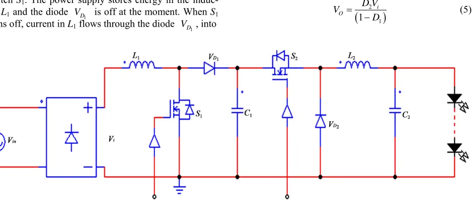
From the non-isolated LED Boost-Buck converter circuit diagram, it can be seen that the converter consists of rec-tifier bridge, boost circuit, buck circuit, driving signal and the load. And the Boost-Buck converter uses ca-pacitor as energy transfer component between the first and post stage rather than the inductor mostly used in other conventional converters. It can be known from the analysis that the Boost-Buck converter features fast tran-sient response and excellent frequency response, allow-ing highly stable feedback regulation to be achieved with simple circuit [15-17]. Two inductors at both input and output side are working in continuous current conduction mode. The inductor ripple current is low and continuous, which can greatly reduce the requirements of input and output filter capacitor. All switch nodes in the circuit are isolated between the two inductors, input and output nodes have no effect on each other, which would make the radiation EMI (Electro Magnetic Interference) from the converter minimized. The operational principles are described and discussed in the next sections.
When the metal oxide semiconductor field effect tran-sistor (MOS-FET) S1 is turned on, current flows through
the rectifier bridge, the input inductor L1 and the MOS
switch S1. The power supply stores energy in the
induc-tor L1 and the diode VD1 is off at the moment. When S1
turns off, current in L1 flows through the diode VD1, into
the capacitor C1 and transfer the energy to storage
ca-pacitor C1 as a power supply for the post stage Buck
converter. When the MOS switch S2 is turned on, current
flows through the capacitor C1, the power switch S2,
in-ductor L2, capacitor C2 and LED strings. Transfer the
energy to the capacitor C2 and provide power supply to
the load LED strings and the diode VD2 is turned off
synchronously. When S2 turns off, current in inductor L2
flows through the LED strings and the free-wheeling diode VD2.
From the analysis it can be known that the average voltage on the inductor L1 is zero as described in
Equa-tion (1).
1 1 1 1
L on L off
V t V t (1)
where on1 and off1 represent the turn-on and the
turn-off time of the MOS switch S1 in a switching period.
According to the operational principle described in the former, Equation (1) can be rewritten as
t t
1
1 1 1
i S C i S
V D T V V D T (2)
where D1 is the duty ratio of S1 and TS is the switching
period. Solving Equation (2) for C1 as shown in
Equa-tion (3), we can see that the output voltage is in-creased much.
V
1
C
V
1
1
1
i C
V V
D
(3)
Taking the same switching period TS and the duty ratio D2 of S2, from the similar analysis of the inductor L2, we
have
VC1VO
D T2 SVO
1D T2
S
(4) Substituting (3) into (4), the relation between output voltage and input voltage can be obtained by
1 2 1i O
D V V
D
[image:2.595.70.540.505.704.2] (5)
From the steady-state operational principle [18], it could be known that the average current flowing through the capacitor C1 must be zero defined as
1 1
C char C unch
I t I t (6)
where char and unch stand for the charging time and
uncharging time respectively. (6) could be rewritten as
t t
1 1 1 2 2
L S L S
I D T I D T (7)
Solving (7) for IL1
2
12 2
1 1
1 1
L O
L
D I D I
I
D D
(8)
3. The Proposed Circuit
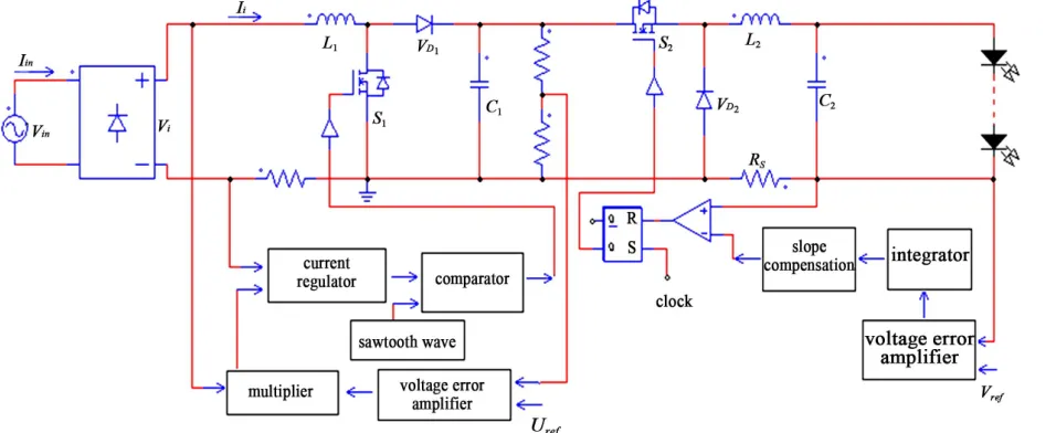
From the analysis of the Boost-Buck converter it can be known that the converter has high stability, fast transient response and high efficiency. But the power factor is low because of harmonic distortion and the use of inductors and capacitors, and it can not satisfy the accurate regula-tion of luminance due to that the light output is propor-tional to the current delivered to the LEDs string aver-aged over the utility period. In order to improve the power factor of the input side of the grid and provide a constant average current and lighting output, the tech-nology of active PFC and ACMC is proposed through adding a PFC control loop and an average current control loop as shown in Figure 2.
The boost PFC circuit operates in CCM with trailing edge modulator, while the leading edge modulation is adopted in the Buck pulse width modulation (PWM) constant average current control circuit. Although the switches work under turned-on and turned-off state al-
ternately, the proposed converter reduces the harmonic current distortion due to the inductors operated in CCM.
From the system block schematic diagram, it can be known that the error signal between the sampled voltage of the capacitor C1 and the reference voltage is amplified
and sent to the analog multiplier for generating a half- sine reference current signal as same frequency and phase as input voltage Vi. The current regulator is used to
compare the sensing current Ii with the half-sine
refer-ence current and then generate a current error amplified signal. Compared with the sawtooth wave, the output of the comparator is the control signal of the MOS switch
S1. Thus, through adjusting the duty cycle, the current of
inductor L1 will track the half-sine reference current
sig-nal that is to say that the input current Iin tracks the
sinu-soidal input voltage Vin well for a high power factor.
To get the working stability of current loop and a good dynamic tracking ability of the average inductor current, the current regulator must be designed to have high low-frequency gain, wide mid-frequency gain, a reason-able margin steady and strong switching ripple suppres-sion ability. A compensation network G(s) with two pole
and one zero is taken as a current regulator as shown in Equation (9).
1
1 i
P
s G s
s s
Z
(9)
where
1 2
1
i i
R C C
, P 11 1 22
C C
R C C
,
1 1
1 Z
R C
.
[image:3.595.67.545.506.702.2]Design goal is to adjust the three parameters to meet the system’s open loop frequency domain index. And the specific implement circuit of the current regulator is shown in Figure 3.
245
To study the discrete control property of the current regulator, a discrete mathematical mode of current sens-ing is created and then transformed into He(s) at the
complex frequency domain.
1 22n z n
s s
He s
Q
(10)
where n S
T
,Qz 2.
[image:4.595.56.227.136.192.2]To avoid aberrance in the inductor current, PFC volt-age error amplifier design can’t seek rapidity excessively and the output voltage should be relatively constant in a frequency cycle. From the perspective of frequency analysis, the voltage regulation loop bandwidth should be limited. And proportional integral voltage regulator is a good candidate and its implement circuit is shown in
Figure 4.
The transfer function of the voltage regulator is
1 z
g Gu s
s s
(11)
where g is the proportional integral coefficient, and
1
2 z
i
C R
according to the stability analysis.
From the system block diagram in Figure 2, we can
see that there is a sensing resistor Rs to sense the output
current. After the output current flowing through the high power LEDs and Rs, the sensing feedback voltage can be
acquired. The integral voltage of error value between the feedback voltage and the reference voltage Vref is sent to
the slope compensation. Compared with the sensing feedback voltage, the comparator output is obtained to control the RS flip-flop and then the output of RS
flip-flop controls the MOS switch S2 and regulates the
[image:4.595.318.539.461.691.2]output average current precisely.
Figure 3. The implement circuit of current regulator.
[image:4.595.104.239.530.594.2]Uref
Figure 4. The implement circuit of voltage regulator.
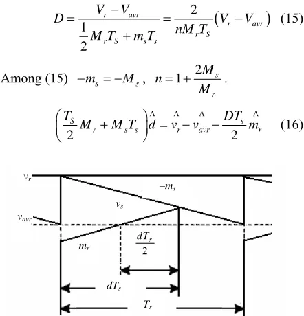
In order to gain the accurate average current, the slope compensation technique is adopted, as shown in Figure 5. r is the reference voltage, and dotted line is
the average voltage of sensing feedback voltage
v vavr
s v in a
switching period. ms, r are the slope of the slope
compensation voltage and the sensing voltage
m
s v
re-spectively. From the steady-state waveforms, it can be seen that the sensing average voltage vavr presents the
average current of high power LED.
re
From the steady-state waveforms, we have
1
2m dTr S vr vavrm dTs s (12)
Take small-signal perturbation of the relevant vari-ables as follows.
r r r avr avr avr
r r r
v V v v V v
m M m d D d
(13)
Among them, the capitalized letters are steady-state values and the variables with “ ” are small-signal dis-turbances.
Substituting (12) into (13), we have
2 S
r r
r r avr avr s
T
M m D d
V v V v m D d T
s
(14)
With ignorance of second-order small-signal variables, we can get the characteristics equations of DC steady-
state (15) and AC small-signal (16).
2 1 2 r avr r avr r Sr S s s V V
D V
nM T M T m T
V
(15)
Among (15) ms Ms,
2 1 s r M n M . 2 2 S s
r s s r avr
T D
r
T
M M T d v v m
(16)
v mr –ms vs vavr r v 2 s dT Ts dTs
Figure 5. The steady-state waveforms with constant average current control.
r
vr
–ms
vs vavr
s dT
mr 2
dTs
[image:4.595.119.224.632.702.2]As a result of the new control technique, the driver provides a precise constant average output current and high power factor under pieces of LED series connection. Moreover, the proposed converter operating in CCM has many better performances such as variable input source voltages, wide frequency bandwidth, high efficiency and stability.
4. Simulation and Experimental Results
To verify the feasibility of the proposed LED driver, a laboratory prototype with the following specifications were designed and tested.
Input voltage: 100 - 240 Vrms
Switching frequency: 200 kHz
LED current: 350 mA
The circuit parameters for the laboratory prototype are as follows: the rectifier sampling coefficient is 0.0032; the inductor L1 = 1.47 mH and L2 = 0.22 mH; the
ca-pacitor C1 = 3500 uF and C2 = 470 uF, the sensing
resis-tor Rs is 0.1 Ω and the reference voltage Vref = 0.035 V.
The series connected LUMILEDS emitter type LEDs is used in this experiment. This LUMILEDS diode is a 1 W high-luminance LED with a nominal forward voltage of 3.42 V. The laboratory prototype is designed to get a high power factor and a constant output average current 350 mA when the input source voltage varies from 100 Vrms to 240 Vrms. Figure 6 shows the tested
wave-forms of the input voltage Vin and input current Iin at the
input source voltage of 110 Vrms and 220 Vrms, respec-tively. It could be seen that Iin has a good near-sinusoi-
dal waveform and in phase with the input source voltage
Vin. Power factor under different input source voltages
variations are shown in Figure 7 and the high power
factor is over 0.95.
(a)
[image:5.595.310.538.181.332.2](b)
Figure 6. The tested input voltage and current waveforms at
Vin = 110 Vrms and 220 Vrms. ((a) The tested input voltage
and current waveforms at Vin = 110 Vrms; (b) The tested
input voltage and current waveforms at Vin = 220 Vrms).
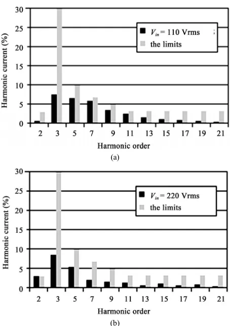
Figure 8 shows that the line-current harmonics are
below the limits set by IEC 61000-3-2 class C
[image:5.595.310.537.361.683.2]regula-tions with enough margin at the input source voltage of 110 Vrms and 220 Vrms, respectively. It can be seen that these high performances such as phase-following, high power factor, low THD are the results of the improved APFC block.
Figure 7. Power factor vs different input voltages.
(a)
(b)
Figure 8. The measured line-current harmonics at Vin = 110
Vrms and 220 Vrms. ((a) Line-current harmonics at Vin = 110
[image:5.595.58.288.508.670.2]247
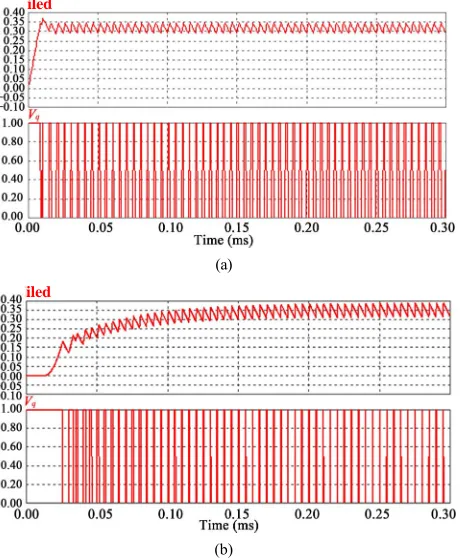
Without the ACMC technique, the LED constant av-erage current is 320 mA below the reference current as shown in Figure 9(a). However, with the proposed
method the constant average current of 350 mA can be achieved as shown in Figure 9(b). It is evident that the
LED average current and luminous flux can be regulated by adjusting the duty cycle of MOS-FET switch. And the steady and slowly-rising LED current of the new driver can protect the MOS switch due to the improved ACMC block.
All the test results are consistent with expectations well.
5. Conclusions
In this paper, we proposed an improved non-isolated LED converter operating in CCM with PFC and ACMC for driving high power LED lamps. A laboratory proto-type with LUMILEDS emitter proto-type LEDs is used to ver-ify the feasibility of the proposed driver. From the meas-ured results, it can be seen that the proposed LED driver achieves a power factor of 0.99 and a THD of 12.2% at input voltage 110 Vrms and a power factor of 0.96 and a THD of 10.4% at input voltage 220 Vrms. Many better
(a)
[image:6.595.60.290.386.665.2](b)
Figure 9. The LED current simulated waveforms and the switching signal. ((a) The LED current simulated waveforms and the switching signal Without the ACMC; (b) The LED current simulated waveforms and the switching signal With the ACMC).
performances such as high power factor, accurate aver-age current control, low current harmonic and switch protection are confirmed and the experimental results match well with the analysis results.
6. References
[1] J. Y. Tsao, “Solid-State Lighting: Lamps, Chips and Ma-terials for Tomorrow,” IEEE Circuits Devices Magazine, Vol. 20, No. 3, 2004, pp. 28-37.
doi:10.1109/MCD.2004.1304539
[2] T. Komine and M. Nakagawa, “Fundamental Analysis for Visible-Light Communication System Using LED Lights,” IEEE Transactions on Consumer Electronics, Vol. 50, No. 1, 2004, pp. 100-107. doi:10.1109/TCE.2004.1277847
[3] R. Mehta, D. Deshpande, K. Kulkarni, S. Sharma and D. Divan, “LEDs—A Competitive Solution for General Lighting Applications,” IEEE Energy 2008, Atlanta, 17-18 November 2008, pp. 1-5.
doi:10.1109/ENERGY.2008.4781063
[4] “Electromagnetic Compatibility (EMC), Part 3-2: Lim-its—Limits for Harmonic Current Emissions (Equipment Input Current ≤ 16 A per Phase),” International Standard IEC 61000-3-2, 2001.
[5] Energy Star Program Requirements for Solid State Light-ing Luminaries. USA, 2007.
[6] J. P. Noon, “Designing High-Power Factor Off-Line Power Supplies,” Proceedings of Unitrode Power Supply Design Seminar Manual SEM1500, Texas Instruments, August 2003, pp. 2-6.
iled
[7] C. K. Tse, “Circuit Theory of Power Factor Correction in Switching Converters,” International Journal of Circuit Theory and Applications, Vol. 31, No. 2, 2003, pp. 157-198.
[8] H. van der Broeck, G. Sauerlander and M. Wendt, “Power Driver Topologies and Control Schemes for LEDs,” IEEE Applied Power Electronics Conference, Anaheim, 25 February-1 March 2007, pp. 1319-1325. [9] G. Spiazzi and J. P. Pomilio, “Interaction between EMI
Filter and Power Factor Pre-regulators with Average Current Control: Analysis and Design Considerations,” IEEE Transactions on Industrial Electronics, Vol. 46, No. 3, 1999, pp. 577-584. doi:10.1109/41.767065
iled
[10] M. Ogata and T. Nishi, “Gragh-Theoretical Approach to 2-Switch DC-DC Converters,” International Journal of Circuit Theory and Applications, Vol. 33, No. 2, 2005, pp. 161-173. doi:10.1002/cta.311
[11] A. Lazaro, A. Barrado, M. Sanz, V. Salas and E. Olias, “New Power Correction AC-DC Converter with Reduced Storage Capacitor Voltage,” IEEE Transactions on In-dustrial Electronics, Vol. 54, No. 1, 2007, pp. 384-397.
doi:10.1109/TIE.2006.888795
doi:10.1109/APEC.1998.647734
[13] M. Rico-Secades, A. J. Calleja, J. Ribas, E. L. Corominas, J. M. Alonso, J. Cardesin and Garcia-Garcia, “Evaluation of a Low-Cost Permanent Emergency Lighting System based on High-Efficiency LEDs,” IEEE Transactions on Industry Applications, Vol. 41, No. 5, 2005, pp. 1386-1390.
doi:10.1109/TIA.2005.853389
[14] Z. Y. Chen, H. L. Yin and P. Li, “Power Quality Problem and New Technology for Its Improvement,” Power Sys-tem Technology, Vol. 26, 2007, pp. 67-70.
[15] M. X. Han, Y. You and H. Liu, “Principle and Realiza-tion of Dynamic Voltage Regulator Based on Line Volt-age Compensating,” Proceedings of the CSEE, Vol. 23, 2003, pp. 49-53.
[16] S. Wall and R. Jackson, “Fast Controller Design for Sin-gle-Phase Power-Factor Correction Systems,” IEEE Trans- actions on Industrial Electronics, Vol. 44, No. 5, 1997, pp. 654-660. doi:10.1109/41.633465
[17] W. Aloisi and G. Palumbo, “Efficiency Model of Boost DC-DC PWM Converters,” International Journal of Cir-cuit Theory and Applications, Vol. 33, No. 5, 2005, pp. 419-432. doi:10.1002/cta.329