warwick.ac.uk/lib-publications
Original citation:
Mizokuchi, R., Torresani, P., Maurand, R., Zeng, Z., Niquet, Y.-M., Myronov, Maksym and De Franceschi, S.. (2017) Hole weak anti-localization in a strained-Ge surface quantum well. Applied Physics Letters, 111 (6). 063102.
Permanent WRAP URL:
http://wrap.warwick.ac.uk/92149
Copyright and reuse:
The Warwick Research Archive Portal (WRAP) makes this work by researchers of the University of Warwick available open access under the following conditions. Copyright © and all moral rights to the version of the paper presented here belong to the individual author(s) and/or other copyright owners. To the extent reasonable and practicable the material made available in WRAP has been checked for eligibility before being made available.
Copies of full items can be used for personal research or study, educational, or not-for-profit purposes without prior permission or charge. Provided that the authors, title and full bibliographic details are credited, a hyperlink and/or URL is given for the original metadata page and the content is not changed in any way.
Publisher’s statement:
This article may be downloaded for personal use only. Any other use requires prior permission of the author and AIP Publishing.
The following article appeared in Mizokuchi, R., Torresani, P., Maurand, R., Zeng, Z., Niquet, Y.-M., Myronov, Maksym and De Franceschi, S.. (2017) Hole weak anti-localization in a strained-Ge surface quantum well. Applied Physics Letters, 111 (6). 063102 and may be found at http://dx.doi.org/10.1063/1.4997411
A note on versions:
The version presented in WRAP is the published version or, version of record, and may be cited as it appears here.
Hole weak anti-localization in a strained-Ge surface quantum well
R.Mizokuchi,1,2P.Torresani,1,2R.Maurand,1,2Z.Zeng,2,3Y.-M.Niquet,2,3M.Myronov,4
and S.De Franceschi1,2,a)
1
CEA, INAC-PHELIQS, F-38000 Grenoble, France
2
University Grenoble Alpes, F-38000 Grenoble, France
3
CEA, INAC-MEM, F-38000 Grenoble, France
4
Department of Physics, University of Warwick, Coventry CV4 7AL, United Kingdom
(Received 12 April 2017; accepted 8 July 2017; published online 8 August 2017)
We report a magneto-transport study of a two-dimensional hole gas confined to a strained Ge quan-tum well grown on a relaxed Si0.2Ge0.8virtual substrate. The conductivity of the hole gas measured
as a function of a perpendicular magnetic field exhibits a zero-field peak resulting from weak anti-localization. The peak develops and becomes stronger upon increasing the hole density by means of a top gate electrode. This behavior is consistent with a Rashba-type spin-orbit coupling whose strength is proportional to the perpendicular electric field and hence to the carrier density. In the low-density, the single-subband regime, by fitting the weak anti-localization peak to an analytic model, we extract the characteristic transport time scales and a spin splitting energyDSO1 meV.
Tight-binding calculations show thatDSOis dominated by a cubic term in the in-plane wave vector.
Finally, we observe a weak anti-localization peak also for magnetic fields parallel to the quantum well and associate this finding to an effect of intersubband scattering induced by interface defects.
Published by AIP Publishing.[http://dx.doi.org/10.1063/1.4997411]
Holes in p-type SiGe-based heterostructures are promis-ing candidates for quantum spintronic applications.1,2 They are expected to display a relatively small in-plane effective mass,3,4 favoring lateral confinement, as well as long spin coherence times, stemming from a reduced hyperfine cou-pling (natural Ge is predominantly constituted of isotopes with zero nuclear spin and holes are less coupled to nuclear spins due to the p-wave symmetry of their Bloch states5). In addition, low-dimensional, SiGe-based structures benefit from a strong and electrically tunable spin-orbit (SO) cou-pling.4,6–10 This property could be exploited to achieve purely electric spin control11,12 which is desirable for spintronic applications such as spin field effect transis-tors,13,14spin-Hall devices,15and spin qubits.16,17
Here, we consider a SiGe-based heterostructure with a compressively strained Ge quantum well (QW) at its surface. This differs from previous studies where buried Ge QWs were investigated.9,18,19 Despite a considerable detrimental effect on mobility, having the Ge well at the surface does present some advantages and opportunities: it allows for more conventional MOSFET-type device structures where, in principle, we can expect to achieve larger electric fields perpendicular to the Ge well and, as a result, higher charge densities, and stronger spin-orbit coupling; it should enable the fabrication of quantum-dot nanostructures with stronger charge confinement and larger level spacing; finally, it will facilitate the development of high-transparency supercon-ducting contacts, thereby opening a new route toward Ge-based superconductor-semiconductor devices, such as Josephson field-effect transistors,20,21 gatemons,22,23 and, possibly, hybrid devices for topologically protected quantum bits based on Majorana fermions or parafermions.21,24
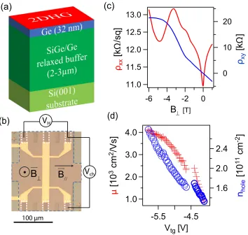
The strained SiGe heterostructure was grown on a 200 mm Si(001) substrate by means of reduced pressure chemical vapor deposition (RP-CVD). Growth was realized using an industrial-type, mass-production system (ASM Epsilon 2000 RP-CVD), which is a horizontal, cold-wall, sin-gle wafer, load-lock reactor with a lamp-heated graphite sus-ceptor in a quartz tube. RP-CVD offers the major advantage of unprecedented wafer scalability and is nowadays routinely used by leading companies in the semiconductor industry to grow epitaxial layers on Si wafers of up to 300 mm diameter. The heterostructures, shown schematically in Fig.1(a), consist of a 3lm thick reverse linearly graded, fully relaxed Si0.2Ge0.8/Ge/Si(001) virtual substrate with a 32-nm-thick
strained Ge QW surface layer. This is a typical design for sur-face channel structures employed in modern MOSFET devi-ces. The full structure was grown in a single process without any external treatment. The surface of the Si wafers was cleaned by anin situthermal bake in H2ambient at high
tem-perature, above 1000C. The Ge epilayer was grown from a commercially available and widely used germane (GeH4) gas
precursor at a relatively low substrate temperature (<450C), as it is known that the growth temperature of the compres-sively strained Ge epilayers has to be sufficiently low to sup-press surface roughening and retain comsup-pressive strain in the epilayers. Further details of material growth and characteriza-tion are described elsewhere.25 The same epitaxial growth technology resulted in the creation of strained Ge QW hetero-structures with superior low- and room-temperature electronic properties26,27 enabling the observation of various quantum phenomena including fractional quantum Hall effects,28 meso-scopic effects due to spin-orbit interactions,2,9,18,29 and tera-hertz quantum Hall effects.30
The studied devices have a Hall-bar geometry defined by a top-gate electrode operated in the accumulation mode [Fig.
1(b)]. Due to the absence of intentional doping, the Ge QW
a)Author to whom correspondence should be addressed:
0003-6951/2017/111(6)/063102/5/$30.00 111, 063102-1 Published by AIP Publishing.
contains no carrier at low temperature. Only by applying a suf-ficiently negative top-gate voltage,Vtg, the accumulation of
a two-dimensional electron gas (2DHG) can be induced in the Ge QW. Device fabrication involves the following steps: a relatively large (tens of microns wide), 55-nm-thick mesa structure is initially defined by optical lithography and dry etching in a Cl2 plasma; ohmic contacts are successively
fabricated using optical lithography, followed by Ar etching (to remove the residual oxide) and Pt deposition in an e-beam evaporator system; 30 nm of Al2O3is deposited
every-where using atomic layer deposition at 250C; finally, the Hall-bar-shaped top gate accumulation electrode is defined by e-beam lithography and deposition of 60 nm of Ti/Au.
Magneto-transport measurements were performed in a
3He cryostat with a base temperature of 300 mK. In the first
set of experimental runs, longitudinal (qXX) and Hall (qXY)
resistivities were measured as a function of the magnetic field, B?, perpendicular to the 2DHG, and Vtg. The onset
of hole accumulation was found to occur at Vtg 4 V, slightly varying from one run to the other. Examples of qXXðB?Þ and qXYðB?Þ traces are given in Fig. 1(c). From
Hall resistivity, we extracted the hole mobility (l) and car-rier density (nhole) ranging from 800 to 4100 cm2=V s and
from 1.3 to 2.8 1011cm2, respectively [data points from
two experimental runs are shown in Fig.1(d)]. The mobility is much lower than the one reported in other strained Ge het-erostructures.27This difference is likely due to the presence of charge traps at the Ge/Al2O3interface.
Following basic Hall-effect characterization, we now turn to a more in-depth investigation of the
magneto-transport properties. In Fig. 1(c), the longitudinal resistivity (red trace) exhibits a pronounced dip at zero magnetic field. Such a dip is a characteristic signature of weak anti-localization (WAL), a mesoscopic phenomenon associated with spin-orbit coupling.31At zero magnetic field, the latter leads to a reduced backscattering resulting in a resistivity minimum. This quantum interference effect is suppressed by a magnetic field perpendicular to the 2DHG, accounting for the observed resistivity dip atB?¼0:
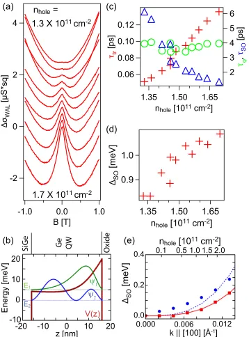
This phenomenon is further investigated as shown in Fig.2(a), where the longitudinal conductivity is now plotted as a function ofB?and for a range ofVtgvalues, after having
removed the feature-less back-ground contribution from classical Drude conductivity. As a matter of fact, DrWAL
represents the quantum correction resulting from WAL. Interestingly, this data set shows that the WAL peak devel-ops and broadens upon increasingVtgand, correspondingly,
the perpendicular electric field and the hole densitynhole in
the QW. All over the nholerange spanned, the 2DHG
occu-pies the first subband only, as confirmed by self-consistent tight-binding (TB) calculations.32 Figure 2(b) shows the valence-band profile calculated for nhole¼1:51011cm2, as well as a representation of the first two hole subbands. From the in-plane dispersion of the first subband (not shown), we obtain an in-plane effective mass m ¼0:07m0,
where m0 is the bare electron mass. This value is slightly smaller, yet close, to those reported in previous studies on buried Ge QWs.9,18,33,34
The evolution of the WAL peak in Fig. 2(a) suggests that the underlying spin-orbit coupling is gate tunable. We
FIG. 1. (a) Schematic of the hetero-structure. (b) Optical image of the Hall bar devices. The blue line highlights the mesa and the white dotted lines the Pt contacts. We measure the transverse Hall voltage (VH) and the longitudinal channel voltage (Vch) from which we extract Hall resistivity and channel resistivity, respectively. The directions of the applied fields B? and B== are
also indicated. (c) Channel resistivity qXX(red) and Hall resistivityqXY(blue)
as a function of the out of plane mag-netic field at Vtg¼ 4.8 V. Channel
resistivity shows a dip at a low field, which is a signature of weak anti-localization. (d) Mobilityl (red) and carrier densitynhole(blue) as a function
of accumulation gate voltageVtg. Data
points above and belowVtg¼ 4:5 V refer to two distinct experimental runs.
[image:3.612.54.408.58.394.2]expect it to be of a Rashba-type since Dresselhaus spin-orbit coupling terms should be negligible due to the existence of bulk inversion symmetry in the Ge QW and surface rough-ness.35The WAL peak can be fitted to the formula36
DrWALðB?Þ ¼
e2
2p2h W
1 2þ
Bu B?
þBSO
B?
þ1
2W 1 2þ
Bu B?
þ2BSO
B?
1
2W 1 2þ
Bu B?
ln Bu
B?
þBSO
B?
1
2ln
Bu B?
þ2BSO
B?
þ1
2ln
Bu B?
; (1)
whereWð ÞX is the digamma function,Buis the phase
coher-ence field, andBSOis the characteristic field associated with
the Rashba spin orbit coupling. From the fitting parameters
BuandBSO, we can extract the phase coherence timesuand
the spin relaxation time sso with si¼m=4phlnholeBi, i
being either u or SO. We note that the large width of the observed WAL peak is consistent with the relatively small values obtained for the scattering time (str ¼ml=e).
These values, as well as those forsu,sSOare displayed as
a function of carrier density in Fig.2(c). The evolution of these characteristic time scales with respect to nholeprovides a hint
on the underlying mechanism for spin relaxation. If spin relax-ation was due to impurity scattering (Elliott-Yafet mecha-nism37,38), thensSOshould increase withstrand decrease with
the carrier density (sso/str=n2hole). This does not correspond
to the observed trend. On the other hand, if spin relaxation occurred in between scattering events, due to spin-orbit-induced rotation (Dyakonov-Perel mechanism39), the spin relaxation time should decrease withstrand with the spin
split-ting energyDSO(sso/1=ðstrD2SOÞ). Our experimental
find-ing is consistent with this second scenario, which allows us to
FIG. 2. (a) Traces of the weak anti-localization contribution to the channel conductivity DrWAL as a function of
B?for different accumulation gate vol-tages and carrier densities from 1:3
1011cm2 (top trace) to 1:71011 cm2 (bottom trace, traces are offset for better visibility). The weak anti-localization peaks emerge as carrier density is increased. (b) Valence band diagram and squared wave functions of the first two hole subbands calcu-lated fornhole¼1:51011cm2. The Fermi energy isEF¼0. (c) Evolution
of scattering time str (red crosses),
phase relaxation time su (green
circles), and spin relaxation timesSO
(blue triangles) as a function of carrier density. (d) Evolution of the spin split-ting energyDSOas a function of carrier
density. (e) Spin splitting energy calcu-lated with a TB model, with and with-out interface roughness (squares and circles) and fits to DSO¼a3E?k3==
(solid and dotted lines, respectively). To simulate the interface roughness, we used a Gaussian auto-correlation function model, with root-mean-square fluctuationD¼0:2 nm and correlation lengthK¼1:0 nm. In this case, the fit reproduces well the TB calculation with a3E?73 eV A˚
3
and a35 105eA˚4
[image:4.612.50.408.51.535.2]deduce the spin splitting energy,DSOhð2ssostrÞ
1=2
, and its dependence on nhole [see Fig. 2(d)]. The obtained values of
DSOare around 1 meV, i.e., a few times larger but still
compa-rable to those reported for similar heterostructures and different experimental methods.9,18,19
In our strained-Ge QW system, where the 2DHG has a predominantly heavy-hole character, we expect the Rashba spin-orbit coupling to be dominated by a cubic term in the in-plane momentum,k==, as also reported in previous
stud-ies.9,18,19,40Figure 2(e) shows a self-consistent TB calcula-tion of DSO k== in a 32-nm thick Ge film saturated by
hydrogen atoms.32We note that the linear/k==dependence
at small k== is quickly overcome by a /k3== dependence.
Interestingly, our calculation shows that for a rough, lower symmetry film, the linear component is almost suppressed (it oscillates rapidly with the film thickness and is averaged down to0 by surface roughness). The calculated values of
DSOappear to be an order of magnitude lower than the
exper-imental values reported in Fig. 2(d). This discrepancy may be ascribed to the simplified description of the surface in the TB calculation, the magnitude ofDSObeing very sensitive to
boundary conditions.
To further investigate the nature of the zero-field con-ductivity enhancement, magneto-transport measurements were performed also with the magnetic field applied in the plane of the 2DHG, as indicated in Fig.3. For first order, an in-plane magnetic field is not expected to break the WAL effect because it produces no flux through the time-reversed back-scattering trajectories. Contrary to this expectation, the longitudinal conductivity measured as a function of the in-plane magnetic field,B==, does exhibit a clear zero-field peak
with a characteristic half width at half maximum of0:7 T, i.e., several times larger than in the case of the perpendicular field.
We can rule out the possibility of a misalignment of the magnetic field with respect to the plane of the 2DHG. In fact, from a simultaneous measurement of the Hall resistiv-ity, also shown in Fig.3, we estimate a misalignment of 2. Therefore, the out-of-plane component of the applied field is far too small to explain the observed WAL peak.
Instead, following Minkov et al.,41 the effect can be ascribed to an effective finite thickness of the 2DHG, and the WAL peak in magneto-conductivity can be expressed as
DrWALB==¼
e2
4p2h 2ln
BuþBSOþDr BuþBSO
þln Buþ2BSOþDr
Buþ2BSO
ln BuþDrþDs
Bu
þS BuþDr BSO
S Bu
BSO
; (2)
where Dr and Ds are B==-dependent corrections toBu taking
into account the effect of surface roughness and Zeeman split-ting, respectively. Following Ref. 41, we assume Dr¼rB2==
and Ds¼sB2==. TheS(x) function in Eq.(2) can be explicitly
written as
S xð Þ ¼ ffiffiffiffiffiffiffiffiffiffiffiffiffiffiffi8
7þ16x
p arctan
ffiffiffiffiffiffiffiffiffiffiffiffiffiffiffi
7þ16x
p
12x
pHð12xÞ
; (3)
where H is the Heaviside step function. For the effective fieldsBSOandBu, we take the values extracted from the
pre-viously discussed magneto-transport measurements in the perpendicular magnetic field, for the same carrier density, i.e.,BSO¼170 mT andBu¼19 mT.
The dotted blue line in Fig.3is a fit to Eq.(2)using the proportionality factors rand sas fitting parameters. The fit shows only moderate agreement with the data. An improved fit can be obtained by introducing in the expression ofDr a
second orbital term proportional to B6
==, i.e., Dr ¼rB 2 ==
þqB6
==, with the additional fitting parameter q. This
sec-ond term describes B==-induced time-reversal symmetry
breaking via the virtual occupation of higher energy sub-bands.42–44The new fit, shown by a solid red line in Fig.3, is in remarkably good agreement with the experimental data set over the entireB==range. Following Ref.43, the value of
the fit parameterqcan be related to the effective thicknessd
of the 2DHG, i.e.,d qU50=4p2n2
hole
1=14
. We find a realis-tic d14 nm, which can be regarded as a sanity check for the model used.
The authors would like to thank M. Houzet, J. Meyer, S. Oda, and M. Sanquer for fruitful discussions. We acknowledge financial support from the Agence Nationale de la Recherche, through the TOPONANO project, from the EU through the ERC Grant No. 280043, and from the Fondation Nanosciences, Grenoble.
1F. A. Zwanenburg, A. S. Dzurak, A. Morello, M. Y. Simmons, L. C. L.
Hollenberg, G. Klimeck, S. Rogge, S. N. Coppersmith, and M. A. Eriksson,Rev. Mod. Phys.85, 961 (2013).
2
C. Morrison and M. Myronov,Phys. Status Solidi A213, 2809 (2016).
3
K. Sawano, K. Toyama, R. Masutomi, T. Okamoto, N. Usami, K. Arimoto, K. Nakagawa, and Y. Shiraki, Appl. Phys. Lett. 95, 122109 (2009).
4C. Morrison, C. Casteleiro, D. R. Leadley, and M. Myronov,Appl. Phys.
Lett.109, 102103 (2016).
5C. Testelin, F. Bernardot, B. Eble, and M. Chamarro,Phys. Rev. B79,
195440 (2009).
6
H. Watzinger, C. Kloeffel, L. Vukusic´, M. D. Rossell, V. Sessi, J. Kukucˇka, R. Kirchschlager, E. Lausecker, A. Truhlar, M. Glaser, A. Rastelli, A. Fuhrer, D. Loss, and G. Katsaros,Nano Lett.16, 6879 (2016).
7N. Ares, V. N. Golovach, G. Katsaros, M. Stoffel, F. Fournel, L. I.
Glazman, O. G. Schmidt, and S. De Franceschi, Phys. Rev. Lett. 110, 046602 (2013).
8
[image:5.612.314.562.54.136.2]C. Kloeffel, M. Trif, and D. Loss,Phys. Rev. B84, 195314 (2011). FIG. 3. Black trace: Hall resistivityqXYas a function of the in-plane
mag-netic field atVtg¼ 5.8 V. The small dependence on field results from a
small perpendicular field component. We estimate an angle of only 2 betweenB==and the chip plane. Black circles: quantum correction to channel
conductivity DrWAL, revealing a weak anti-localization peak. The blue dashed line and the red solid line are fits to the model from Minkovet al.41
without and with the addition of aB6
==term, respectively.
[image:5.612.83.265.590.694.2]9C. Morrison, P. Wisniewski, S. D. Rhead, J. Foronda, D. R. Leadley, and
M. Myronov,Appl. Phys. Lett.105, 182401 (2014).
10
A. Zarassi, Z. Su, J. Danon, J. Schwenderling, M. Hocevar, B.-M. Nguyen, J. Yoo, S. A. Dayeh, and S. M. Frolov, “Magnetic field evolution of spin blockade in Ge/Si nanowire double quantum dots,” Phys. Rev. B 95, 155416 (2017).
11
N. Ares, G. Katsaros, V. N. Golovach, J. J. Zhang, A. Prager, L. I. Glazman, O. G. Schmidt, and S. D. Franceschi,Appl. Phys. Lett. 103, 263113 (2013).
12
V. N. Golovach, M. Borhani, and D. Loss, Phys. Rev. B 74, 165319 (2006).
13S. Datta and B. Das,Appl. Phys. Lett.56, 665 (1990). 14D. D. Awschalom and M. E. Flatte,Nat. Phys.
3, 153 (2007).
15
T. Jungwirth, J. Wunderlich, and K. Olejnık,Nat. Mater.11, 382 (2012).
16
K. C. Nowack, F. H. L. Koppens, Y. V. Nazarov, and L. M. K. Vandersypen,Science318, 1430 (2007).
17R. Maurand, X. Jehl, D. Kotekar-Patil, A. Corna, H. Bohuslavskyi, R.
Lavieville, L. Hutin, S. Barraud, M. Vinet, and M. Sanquer, Nat. Commun.7, 13575 (2016).
18M. Failla, M. Myronov, C. Morrison, D. Leadley, and J. Lloyd-Hughes,
Phys. Rev. B92, 045303 (2015).
19
R. Moriya, K. Sawano, Y. Hoshi, S. Masubuchi, Y. Shiraki, A. Wild, C. Neumann, G. Abstreiter, D. Bougeard, T. Koga, and T. Machida,Phys. Rev. Lett.113, 086601 (2014).
20J. Xiang, A. Vidan, M. Tinkham, R. M. Westervelt, and C. M. Lieber,Nat.
Nanotechnol.1, 208 (2006).
21
Z. Su, A. Zarassi, B.-M. Nguyen, J. Yoo, S. A. Dayeh, and S. M. Frolov, “High critical magnetic field superconducting contacts to Ge/Si core/shell nanowires,” preprintarXiv:1610.03010(2016).
22
G. de Lange, B. van Heck, A. Bruno, D. J. van Woerkom, A. Geresdi, S. R. Plissard, E. P. A. M. Bakkers, A. R. Akhmerov, and L. DiCarlo,Phys. Rev. Lett.115, 127002 (2015).
23L. Casparis, T. W. Larsen, M. S. Olsen, F. Kuemmeth, P. Krogstrup, J.
Nyga˚rd, K. Petersson, and C. M. Marcus,Phys. Rev. Lett.116, 150505 (2016).
24F. Maier, J. Klinovaja, and D. Loss,Phys. Rev. B90, 195421 (2014). 25
M. Myronov, A. Dobbie, V. A. Shah, X.-C. Liu, V. H. Nguyen, and D. R. Leadley,Electrochem. Solid-State Lett.13, H388 (2010).
26A. Dobbie, M. Myronov, R. J. H. Morris, A. H. A. Hassan, M. J. Prest, V.
A. Shah, E. H. C. Parker, T. E. Whall, and D. R. Leadley, Appl. Phys. Lett.101, 172108 (2012).
27M. Myronov, C. Morrison, J. Halpin, S. Rhead, C. Casteleiro, J. Foronda,
V. A. Shah, and D. Leadley,Jpn. J. Appl. Phys., Part 153, 04EH02 (2014).
28
Q. Shi, M. A. Zudov, C. Morrison, and M. Myronov,Phys. Rev. B91, 241303 (2015).
29J. Foronda, C. Morrison, J. E. Halpin, S. D. Rhead, and M. Myronov,
J. Phys.: Condens. Matter27, 022201 (2015).
30
M. Failla, J. Keller, G. Scalari, C. Maissen, J. Faist, C. Reichl, W. Wegscheider, O. J. Newell, D. R. Leadley, M. Myronov, and J. Lloyd-Hughes,New J. Phys.18, 113036 (2016).
31W. Knap, C. Skierbiszewski, A. Zduniak, E. Litwin-Staszewska, D.
Bertho, F. Kobbi, J. L. Robert, G. E. Pikus, F. G. Pikus, S. V. Iordanskii, V. Mosser, K. Zekentes, and Y. B. Lyanda-Geller,Phys. Rev. B53, 3912 (1996).
32Y. M. Niquet, D. Rideau, C. Tavernier, H. Jaouen, and X. Blase,Phys.
Rev. B79, 245201 (2009).
33
M. A. Zudov, O. A. Mironov, Q. A. Ebner, P. D. Martin, Q. Shi, and D. R. Leadley,Phys. Rev. B89, 125401 (2014).
34D. Laroche, S.-H. Huang, Y. Chuang, J.-Y. Li, C. W. Liu, and T. M. Lu,
Appl. Phys. Lett.108, 233504 (2016).
35
L. E. Golub and E. L. Ivchenko,Phys. Rev. B69, 115333 (2004).
36S. Iordanskii, Y. B. Lyanda-Geller, and G. Pikus, ZhETF Pisma
Redaktsiiu60, 199 (1994).
37
R. J. Elliott,Phys. Rev.96, 266 (1954).
38
Y. Yafet,Phys. Lett. A98, 287 (1983).
39M. Dyakonov and V. Perel, Sov. Phys. Solid State, USSR 13, 3023
(1972).
40
R. Winkler, D. Culcer, S. J. Papadakis, B. Habib, and M. Shayegan, Semicond. Sci. Technol.23, 114017 (2008).
41G. Minkov, A. Germanenko, O. Rut, A. Sherstobitov, L. Golub, B.
Zvonkov, and M. Willander,Phys. Rev. B70, 155323 (2004).
42
V. I. Fal’ko,J. Phys.: Condens. Matter2, 3797 (1990).
43
J. S. Meyer, A. Altland, and B. L. Altshuler,Phys. Rev. Lett.89, 206601 (2002).
44