Technical Manual Revision A, August, 1981 CENTRAL PROCESSING UNIT 803439
CONTENTS 1. GENERAL
Features
2. PHYSICAL DESCRIPTION Power-On-Jump Option 3. FUNCTIONAL DESCRIPTION
Timing Microprocessor Reset
Power-On-Jump Input Output Ports Interrupts
4. SPECI FICA TlONS . 5. INSTAllATION
Options
6. MAINTENANCE
Customer Support Service 7. REFERENCE
S-100Bus
Schematics and Replaceable Parts Engineering Change Orders
ILLUSTRATIONS
Figure 2-1 - Central Processing Unit - 803439 Figur~ 2·2 - CPU I/O Cable - 800285
Figu(e 3-1 - Central Processing Unit Functional Block Diagram
Figure 3·2 - Central Processing Unit Timing
MAINTENANCE
PAGE 1 1 2 4 4 4 4 7 7 7 9 21 23 23 24 24 24 24 24 24
PAGE
3
4
5 6
I LLUSTRA TlONS PAGE
Table 4·1 - Central Processing Unit 803439
Specifications 21
Table 7·1 - Dynabyte S-100 Bus Pin Assignments. 25 Figure 7-1 - Central Processing Unit Logic Diagram 30 Table 7-2 - Central Processing Unit Replaceable
Parts List
Table 7·3 - CPU Serial and Parallel I/O Port Pin Assignments
1. GENERAL
31
36
1.01 This manllal provides a physical and func-tional dpsniption and Llw opprating tIwory I1P('('ssary for t'ffectiv(' fit'ld s!'rvice of til(' (\'ntral Procl>ssing Unit (CPU) 80:3439. 'flIP CPU is sup-pJipd in t1w DynabyLt· 5100/5200 Computl-r Units. Features
1.02 The CPU is dpsignl'd for oIwration in tilt'
Dynabyte S-IOO Bus. F('atures of the CPU include:
•
•
•
A Z80 microprocessor.
Switch-optioned Powpr-On-Jump to any 4K hytt- boundary.
Two software baud raLe selectable I/O ports .
. Table ;-1 - S-l00 Bus Signals Used By The CPU 8 Table ;-2 - CPU I/O Port Address and Function 11
• I/O ports may be eith(-r RS-232C or 20 m.A current loop interface.
_,I DVlhlb .... lt·, Inc., l~jH)
PrJnlt'd 111 l'.S.A.
• OIW TTL 8-bit parallel I/O port with Strobe
and Data Ready lines.
• Solder masked pc board.
• Each CPU carries 3~-day wananty on parts and labor.
• Each CPU pc assembly (PCA) is burned in for a minimum of 72 hours.
1.03 Operational features of the Dynabyte S-100 Bus are described functionally in both the 5100 and 5200 Computer Technical Manuals. Table 7-1 in this manual summarizes the Dynabyte S-100 Bus pins by assignment and function.
1.04 Dynabyte maintains hardware and software compatibility with the Dynabyte S-100 Bus only. The CPU may not operate with all S-100 Bus computers. Contact Dynabyte, Inc., for specific applications.
2_ PHYSICAL DESCRIPTION
2.01 The CPU is an integrated plug-in unit incorporating all the necessary components for a high-speed S-100 Bus processor including I/O ports. This printed eircuit assembly (PCA) contains:
(1) A Z-80 microprocessor.
(2) A 8 MHz crystal-controlled dock for timing signals.
(3) A latch to hold status information.
(4) Lint" drivers and receivers connected to the S-100 Bus.
(5) Voltage regulators for powering the CPU logic.
Figure 2-1 illustrates the CPU.
Page 2
2.02 The PCA measures 5 x 10 inches. A 100-pin edge connector mates with the S-100 Bus connector of the 5100/5200 Computer mother-board. This connector is offset by 5/8 inch from the pc board centerline, i.e., the PCA cannot be inserted into the motherboard backwards.
2.03 Distinctive white s.ilkscreened marking has been provided on the component side of the PCA.
(1) The card name, Dynabyte part number and a location for the serial number have been marked on the pc board. Some early CPUs have the serial number etched on the pc board.
(2) Component reference designators are marked where practical. They facilitate locating the individual part on the schematic or replaceable parts list. Refer to Part 7.
The CPU integrated circuits and some major components derive their reference designators from the row-column matrix silkscreened onto the pc board. Refer to Figure 2-1. Rows are A to C and columns are 1 to 15. An integrated circuit located at the lower right corner is C15.
2.04 The PCA has three on-board regulators located at AI, B1 and C14.
(1) B1 provides +12 Vdc and is provided with an insulated heat sink.
(2) Al provides +5 Vdc and is provided with an insulated heat sink.
(3) C14 provides -5 V dc and is provided with an insulator.
If it becomes necessary to change one of these regulators, coat the mating surface with a thermal conductive cream. Secure the regulator to the surface with a screw and nut.
NOTE
The peA should nel'er be inserted or removed from the bus when the ac line is cOllnected
[image:2.630.56.598.294.741.2]\
~{:Pl'
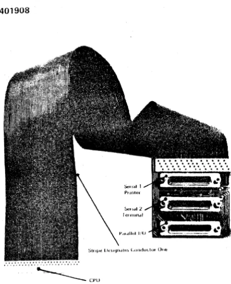
Figure 22 - CPU Port 1/0 Cable --800285
2.05 Tlw Ibn'(' groups of I/O port :;igllals an' i'x,·hallg.·d with 1.111' ,'xt('rnal data t"rIlllllals ovpr a 5()-"UIH!lH:tor COllllPclor l()call~d along the top edgt.>. 'l'lw (~PU I/O Cable, R00285, maL,'s with this COIIIH'l:tor and t.'xtl'nds the signals to lilt' r('ar panel of tht' f)100/5200 Computer Unit. 'fhi:; is a
50-conductur flat cahlt,.
IMPORTANT
ilJlllli-col/duuor I/O cables a«' po/ariz/'ll wilh (/ 1'(/ ill led Sf rip II II ('II 1/ tf II {' lor () lit'. 1'h is
. (".I-)ndue l(Jriste~rmillalt'-dal PillOue .oflht'
(·olll/I'ctor. 1'his marking ('/JIlI't'lIliol/ serl'n
II) polarize lIlilling (·OIIl/('C/OfS.
Power-On-Jump Option
2.06 ,\ fiw-position DIPswitch locatl'd at ,\7 and dl'slgnal"d SWI p .. rfonns two functIOns: (1) Pusltions 1 to 4 St't Uw high orth~r fuur-bit
addn':;:; wlwn P()W(~r-OIl-Jllmp option is ,'n"blt-d . . \1 ;), A14, ;\1:3 and A12 correspond
to 5 to ~ silkscret'ncd Iwxt to t1w switch. (~) PU;;ltl()1l [) enables the t'owl'r-()n-,Jump f"at uri'. The switch is opell in Dynabyte Disl-.. Storagt' Systems.
Page 4
3. FUNCTIONAL DESCRIPTION
3.01 Tlw basic function of a Central Processing Unit (CPU) within a computer system is to accept data and instructions, perform the opt'fations and deliver data back out.
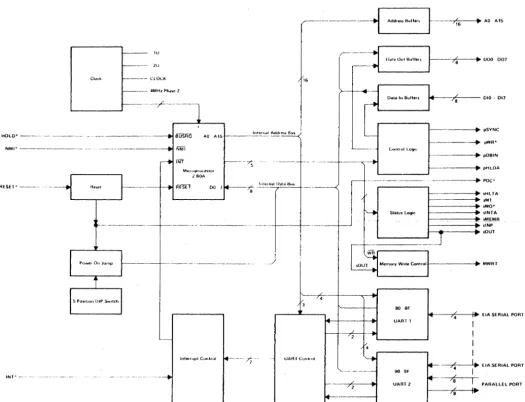
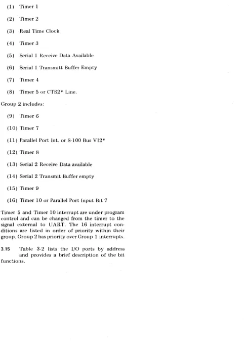
3.02 Figure 3-1 illustrates CPU S03439 in block dia!,,'l'am and should be used in conjunction with the CPU logic diagram in Part 7 for the description which follows. Table· 3-1 tabulates the S-IOO Bus signals used by the CPU.
NOTE
.1 * .mlfix /0 a signa/name il1dicatt's a logical
NOT alld active low.
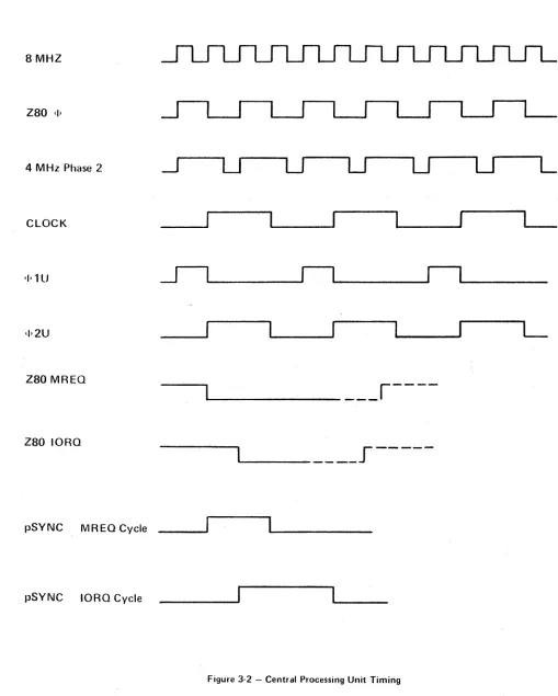
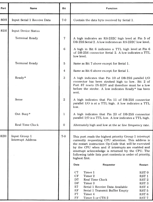
Timing
3.03 CLOCK -- An 8 MHz crystal-controlled oscillator establishes the timing reference; for the CPU and the 8-100 Bus.
(l) III is the timing reference for UART l. The UART divides this signal down to a software-controlled data communication line rate of from 110 to 76,800 baud.
(2) 2U is the timing reference for UART 2. Its function is similar to (1) above.
(3) CLOCK is a 2 MHz 40% - 60% duty cycle clock supplied to the S-100 Bus.
(4) 4 MHZ PHASE 2 is the master timing signal supplied to the S-100 Bus.
(5) 'I) is supplied to the microprocessor. Refer to Figure 3-2.
Microprocessor
3.04 The principle element of the CPU is the Microproct!sso/' (J.1P). It addresses other CPU elements over an internal 16-Bit Address Bus.
(1) A tldress Huff"r.\ - are tri-state device~
which cOl1lwd to the S-lOO Address Bus, AO -~ A15.
(2) UARTI. llN.L' IIl1d COlltrol - for data
[image:4.615.75.304.53.335.2]- - - - III
- _ . - - _ .. ]11
--r.----+
UOO 007
Clu.:k -.----.-- ClOCK
16
---/--- ~DIO-DI1
tnle'"dl Add"H~ Bu~
AO A15 - - - . - - - .
MI<:,upr"u~u(J'
i 80A
---+ pWR---... - - + pD81N - - - , , - - - . pHLDA
RESEl' - - - - . DO I
--1
h,ltorllOjI Data H .. ~ - - - .
POe-Slatu~ Logic
80 8F
UARll
tJAH I ClJlltfUl
90 9f
INf'
---UART 2
.---+ sHlTA ---+ sM1
- - - - + s W O ·
- - - _ . s I N T A
---~.~,. _s~~~R
1---.
slNP1-_---.
sOUlI+---,;~i--II~. EIA SERIAL PORl 1
---;rf--~ E1ASERIAl PORT 'J • I
/
I -PARAllEl PORT
I---;,-.;i-~I.
Figure 3-1 - Central Processing Unit Functional Block Diagram
Communications are handled by an 8-Bit bi-directional data bus. The internal data bus is tri-state.
(3)
Data III BuJJers - connect to 8-100 BusData In Lines 010 -- 017.
(4) Data (Jut Buffers -- connect to 8-100 Bus
Data Out Lines 000 - 007.
(5) UART I. UART 2 -- for data
communi-cations.
(6) Power-Oil-Jump where it conveys the
jump address when this featUre is enabled. Refer to 3.07.
The pP initiates five control signals to the 8-100 Bus from Coutrol Logic during processing
operations. The COlltrol Logic consists of data latches.
(7 ) p8YNC identifies
processing cycle.
the beginning Refer to Figure
of a 3-2.
(8) pWR* signifies the presence of valid data on the Data Out Bus, 000 - 007.
(9) pOBIN requests data from the Data In Bus, OW - 017.
(10) pHLOA is used in conjunction with HOLO* to coordinate bus master transfer operations.
(11) MWRT is the write to memory.
[image:5.621.35.560.51.453.2]8MHZ
Z80 <I>
4 MHz Phase 2
---1
U
U
U
U
U
L
CLOCK
J
L
(1·1U
I I
n
n
·1>2U
L
Z80 MREO
~
____________
r----Z80 IORO
'---
.r---pSYNC MREO Cycle
[image:6.612.69.578.80.715.2]. pSYNC IORO Cycle
Figure 3-2 - Central Processing Unit Timing
In addition, tlw 11 P supplies seven status lines to the S-IOO Hus from Status l.ogic during processing operations. The Status Logic consists of latches.
(12) sHLTA acknowledges a lILT instruction has been executed.
(13) sMI indicates the current cycle is an op-code feteh.
(14) sWO* identifies a bus cycle which transfers data from the CPU to a device.
(15) slNTA identifies the bus input cycle(s) that may follow an accepted interrupt request presented on 8-100 Bus INT* Line.
(16) sMEMR identifies the bus input cycle(s) which transfer data from memory to the CPU which are not interrupt acknowledge instruction fetch cycle( s).
(17) sINP indicates the data transfer bus cycle is from an input device.
(IS) sOUT indicates the data transfer bus cycle to an output device.
3.05 Two S-IOO Bus lines are input directly to the I1P.
(1) HOLD* is the Hold Request line and is used by temporary bus masters to request con-trol of the bus from the CPU. Refer to 3.04 (10) above.
(2) NMI* is the non-maskable interrupt. It has priority over the maskable interrupts. Refer to 3.14.
Reset
3.06 The Reset may be activated in either of two ways.
(1) An S-IOO Bus request reset is received. The RESET line goes low, e.g., when the computer operator keys the Front Pant'! RESET.
(2) AC power is applied to the computer system.
A Power On Clear (POC) is issued from Reset
to the 8-100 Bus I'OC* line and the CPU Power On
.lulII[1 circuit. POC* is the master reset line for the
Dynabytl' system.
Power·On·Jump
3.07 Option switches on the CPU provide a starting addrpss for the CPU after a POC* is issued. The Powt'r On .l1I1II1} provides for the I1P
to jump to any high-order 4-Bit address enabled and set by the !i-position I)lP Switch. This starting address is output to the 11 P over the internal data bus.
Input Output Ports
3.08 1I ART COil tro/ monitors status and supplies
controls to two' input output (I/O) ports on the CPU.
(1) UART 1 - address SOH to SFH is a serial port.
(2) UART 2 -- address 90B to 9FH can be configured to be a serial port and as-Bit parallel port.
Both of these ports have their operating parameters, e.g., baud rate, parity check, seri;;tl or parallel operation through software. The Operating System initializes the I/O ports when the system is reset.
3.09 1 wo serial data communications configura-tions are supported by the UARTs.
(1) 20 mA current loop.
(2) EIA RS-232C Data In, Out and Signal Common. Terminal' Ready is monitored at Pin 5 of the DB-25S connector. All these lines are at RS-232C voltage levels. Modem control and statu~ lines are at TTL levels.
Table 7-3 tabulates the Rear Panel DB-25S recep-tacle pin assignments for these ports.
3.10 CPU strap options provide for setting four modem control lines to RS-232C high or low. These are labeled on Figure 7-1, CPU schematics, as:
(1) RTS1*
(2) DTR1 *
Name
4 MHZ PHASE 2
AI·· A15
ADSB*
CLOCK
DIO -.. DI7
DOO D07
DODSB*
MWRT
NMI*
POC*
RESET*
VI2*
pDBIN
pHLDA
HOLD*
pINT*
pSYNC
pWR*
sHLTA
slNP
Page 8
Table 3-1 S 100 Bus Signals Used By The CPU
Pin
24
Various
22
49
~
Various
Various
23
68
12
99
75
6
78
26
74
73
76
77
48
46
Function
The master timing signal for the bus.
Adtln>ss bits 0 through 15.
The control signal to disable the 16 address sib>'J1als.
2 MHz (0.5'1<.,) 40% -. 60% duty cycle. Not required to be synchronous with any other bus signal.
Data in hits 0 through 7.
Data ou L biLs 0 through 7.
The control signal to disable the 16 address signals. ,~
A bus memory write signal. pWResOUT* (logic equation). This signal must follow pWR* by not more than 30 ns.
Nonmaskablt~ illt(~rrupt.
The Master l{,eseL signal. The Power-On-Clear signal for all devices. Wh"tl this signal goes low, it must stay low for at least 10 ms.
Requpsts the reset of all bus master devices. Connects to the Front Panel Reset Switch and activates POC*.
Vectored interrupt line 2.
The control signal that request data on the DJ bus.
A control signal used in conjunction with HOLD* to coordinate bus master transfer operations.
The control signal used in conjunction with pHLDA to coordinate bus master transfer operations.
The primary interrupt request line.
The control signal identifying the beginning of a processor cycle.
The control signal signifying the presence of valid data on DO bus.
The status signal which acknowledges that a HL T instruction has been executed.
[image:8.623.59.587.78.768.2]Table 3-1 - S-100 Bus Signals Used By The CPU (Continued)
Name
sINTA
sM1
sMEMR
sMREQ*
sOUT
sRFSH*
sWO*
(3)RTS2*
(4) DTR2*
Pin
96
44
47
65
45
66
97
Function
The status signal identifying the bus input cycle(s) that may follow an accepted interrupt requested presen t on INT*.
The status signal which indicates that the current cycle is an op-code fetch.
The status signal identifying bus cycles which transfer data from memory to a bus master, which are not interrupt acknowledge instruction fetch cycle(s).
The status signal identifying bus cycles which reference memory read, write or refresh.
The status signal identifying the data transfer bus cycle to an output device.
The status signal identifying the current address on AO - A6 is a dynamic memory refresh address.
The status signal identifying a bus cycle which transfers data from a bus master to a slave.
(9) FLAT2 OUT*
3.12 Ten interval timers are part of the two Part 5 explains the installation procedure.
UARTs. Each timer may be counted down from a programmed count of 1 to 255. Each count is 64 ps, resulting in intervals of 64 ps to 16.32 ms. At zero an interrupt pending bit is set and under program control can generate an interrupt to the pP.
3.11 An 8-Bit parallel I/O port is also supported by V ART 2. The input lines are:
(1) INO _. IN7, the Data In lines,
(2) READY*
(3) SENSE
(4) PORT*
(5) OUTBUSY*
The output lines are:
(6) OUTO - OUT7, the Data Out lines,
(7) OUT STROBE
(8) FLAG10UT*
3.13 Pin 55, Real Time Clock, of the S-100 Bus is monitored. R TC is at the ac line frequency. It's sine wave undergoes wave shaping and is supplied to VA RT I sense input. The sense input can be programmed to set a status bit or cause an interrupt in synchronism with the ac line frequency. The Operating System may use this for time-of-day applications.
Interrupts
3.14 In addition to INT*, the maskable interrupt, and NMI*, the non-maskable interrupt, supplied from the S-100 Bus, the UARTs provide the CPU with sixteen individually maskable inter-rupts. Group 1 includes:
(1) Timer 1
(2) Timer 2
(3) Real Time Clock
(4) Timer 3
(5) Serial 1 Receive Data Available
(6) Serial 1 Transmitt Buffer Empty
(7) Timer 4
(8) Timer 5 or CTS2* Line.
Group 2incl-udes:
(9) Timer 6
(10) Timer 7
(11) Parallel Port Int. or S-100 Bus V12*
(12) Timer 8
(13) Serial 2 Receive Data available
( (14) Serial 2 Transmit Buffer empty
(15) Timer 9
(16) Timer 10 or Parallel Port Input Bit 7
Timer 5 and Timer 10 interrupt are under program control and can be changed from the timer to the signal external to UART. The 16 interrupt con-ditions are listed in order of priority within their group. Group 2 has priority over Group 1 interrupts.
3.15 Table 3-2 lists the I/O ports by address and provides a brief description of the bit functions.
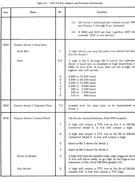
[image:10.620.45.527.58.748.2]Table 3-2 - CPU I/O Port Address and Function
Port Name Bit Function
80H Input Serial 1 Receive Data 7-0 Contain the data byte received by Serial 1.
81H Input Device Status
Terminal Ready 7 A high indicates an RS-232C high level at Pin 5 of OB-25S Serial 2. A low indicates an RS-232C low level.
6 A high in Bit 6 indicates a TTL high level at Pin 6 of OB-25S connector Serial 2. A low indicates a TTL low level.
Terminal Ready 5 Same as Bit 7 above except for Serial l.
4 Same as Bit 6 above except for Serial 1.
Ready * 3 A high indicates that Pin 10 of OB-25S parallel I/O connector has been strobed high to low_Bit 2 of Port 87 resets IN-ROY and therefore must be a low before the strobe. A low indicates Ready* has been sent.
Sense 2 A high indicates that Pin 11 of OB-25S connector parallel I/O is at a TTL high. A low indicates a TTL low.
Out Busy* 1 A high indicates that Pin 23 of OB-25S connector parallel I/O is a TTL low. A low indicates a TTL high.
Real Time Clock 0 Alternately high and low at the ac line frequency rate.
82H Input Group 1 7-0 This port reads the highest priority Group 1 interrupt Interrupt Address currently requesting CPU attention. This address is the restart instruction Op-Code that will be executed by the CPU when and if interrupts are enabled and interrupt acknowledge is returned by the CPU. The following table lists port contents in order of priority, highest first.
Data Requestor Restart
C7 Timer 1 RSTO
CF Timer 2 RST 1
07 Real Time Clock RST2
OF Timer 3 RST3
E7 Serial 1 Receive Data Available RST4 EF Serial 1 Transmit Buffer Empty RST5
F7 Timer 4 RST6
FF Timer 5 or CTS 2 RST 7
Table 3·2 - CPU I/O Port Address and Function (Continued)
Port Name
8aH Input Serial 1 Status
Page 12
Start Bit Detect (SBD)
Full Bit Detect (FBD)
Interrupt Pending (IPB)
Transmit Buffer Empty (TBE)
Received Data Available (RDA)
Serial Received (SRB)
Overrun Error (ORE)
Bit
7
6
5
4
3
2
1
Function
This port can be used to service interrupts by polling. After reading, the highest priority interrupt is reset.
If none are pending OFFH will be read. When interrupts re-enabled and unmasked, the indicated restart instruction will be executed.
A high indicates that Serial 1 has received the start bit . . . Th' bit . h· i h until ofanmcommgcharacter.. IS..I.emamS ... 19I .... ' ... __ _ the entire character is received or until a reset command is issued. This bit is used for testing.
This bit is identical to bit above except that it indicated the first data bit ill an incoming character instead of the start bit.
A high indicates that one or more Group 1 interrupts have been requested and are unmasked. This bit is high when a Group 1 hardware interrupt is requested of the CPU. This bit is used to service interrupts via polling.
A high indicates that Serial 1 Transmit Buffer is ready to accept a character. The Serial Transmitter is buffered and the user may load a new character even before the previous character is totally transmitted. TBE is set high by the reset command and can request a Group 1 interrupt.
RDA is set high when the Serial 1 Receiver buffer is
loaded with a new character and remains high until the buffer is read or a reset Serial 1 command is received.
If the buffer is not read before the next character is received, the new character will overwrite the old and set the overrun error flag. RDA can request a Group 1 interrupt.
Monitors the Serial 1 Data Input Signal which pro-vides break character detection. A high indicates a high at the Serial Data Input and a low indicates a low.
[image:12.617.47.571.81.755.2]Port
84H
Table 3-2 - CPU I/O Port Address and Function (Continued)
Name Bit
Frame Error (FEB)
o
Output Signal Serial 1 Command
7
6
Test (TB5) 5
High Baud (HBR) 4
INTA Enable (INE) 3
INT7 Select (INT7) 2
Break (BRK) 1
Reset (RST)
o
Function
A high indicates that an incorrect number of stop bits have been received on Serial L FEB is cleared each time Port 83H is read or when a reset Serial 1 command is received.
Bits 5 - 1 are latched.
Unused.
Unused.
TB5 is a test bit that should be low at all times. TB5 is latched between outputs to Port 84H.
A high multiplies the Serial 1 standard baud rate by 8 and divides the standard count rate by 8. A low sets the standard baud rate and count. HBR is latched between outputs to Port 84H.
A high will enable Group 1 unmasked int~rrupts to gate a restart instruction to the processor during interrupt acknowledge time. A low IN E will cause no restart instruction to be gated even though an inter-rupt has bet'n generated. An interinter-rupt with no gated restart instruction will default to RST7. INE is latched between outputs to Port 84H.
A high connects an Interrupt 7 (RST7) request to the low to high transition of RS-232C signal Serial 2 Terminal Ready. A. low at IN7 connects Interrupt 7 to Timer 5 zero count. IN7 is latched between outputs to Port 84H.
A high will cause Serial 1 Transmitter to send a Break character (continuous spacing). A low will set Serial 1 to normal operation. If RST and BRK are both high, RST will override (see below)_ BRK is latched between outputs to Port 84H.
A high will:
(1) Clear Serial 1 receive register and set low: SBD, FBD, RDA, ORE and FEB. Receive buffer will contain last received character.
(2) Serial 1 transmitter data output is set high (marking) and TBE is set high.
[image:13.617.43.558.87.739.2]Table 3-2 - CPU I/O Port Address and Function (Continued)
Port Name
85H Output Serial 1 Baud Rate
Stop Bits
Rate
86H Output Serial 1 Transmit Data
87H Output Device Control Word
Reset In-Ready
Out Strobe
Page 14
Bit
7
6-0
Function
(3) All Group 1 interrupts are cleared except TBE and Timers 1 through 5 are inhibited.
(4) If BRK and RST are high together, RST will override. RST is not latched.
A high selects one stop bit and a low selects two stop bits for Serial 1.
A high in Bit 6 through Bit 0 selects the indicated Serial 1 baud rate as standard or high depending on HBR of Port 84H. If niore than one bit is high, the highest rate will prevail.
6 9,600 or 76,800 baud 5 4,800 or 38,400 baud 4 2,400 or 19,200 baud 3 1,200 or 9,600 baud 2 300 or 2,400 baud 1 150 or 1,200 baud
o
110 or 880 baud7-0 Loaded with the data byte to be transmitted on Serial 1.
All bits are latched between Port 87H outputs.
7 A high will output a TTL low at Pin 4 of DB-25S connector Serial 2. A low will output a high.
6 A high will output a TTL low at Pin 20 of DB-25S connector Serial 2. A low will output a high.
5 Same as Bit 7 above for Serial 1.
4 Same as Bit 6 above for Serial 1.
3
2
A high will reset the parallel ready edge triggered latch. A low will allow ready to go high on the high-to-Iow transition of Pin 10 of DB-25S parallel I/O.
[image:14.624.43.557.60.757.2]Port
88H
89H
8AH
8BH
Table 3·2 - CPU I/O Port Address and Function (Continued)
Name Bit
. Flag 2 Out* 1
Flag 1 Out*
o
Output Group 1 Interrupt Mask
Timer 5 or Serial 2 Terminal 7
Ready
Timer 4 6
TBE (Serial 1 ) 5
RDA(~ri~l) 4
TIm~3 3
Real Time Clock 2
Timer 2 1
Timer 1 0
Output Timer 1 Count
7-0
Output Timer 2 Count
7-0
Output Timer 3 Count
7-0
Function
A high will output a TTL low at Pin 25 of DB-25S parallel I/O. A low will output a TTL high.
A high will output a TTL low at Pin 12 of DB-25S parallel [/0. A low will output a TTL high.
Each bit of the Group 1 interrupt mask corresponds to one of the eight Group 1 interrupts. A high will pnable and a low will inhibit that interrupt. The interrupt request is latched independently of the mask and therefore will remain active if masked until a reset occurs or the mask is changed and the interrupt acknowledged.
This port is loaded with the count to start Timer 1.
The count is then decremented by one every 64 micro-seconds until zero. At zero an interrupt is requested at the priority level of the timer if it is unmasked. Maximum time interval is 255 x 64 IlS
=
16.32 ms. Loading a zero will cause an immediate interrupt request. A count may be changed any time. If the HBR bit of Port 84H is high, the count rate is 8 IlSinstead of 64 for Timers 1 through 5.
Same as Port 89H for Timer 2.
Same as Port 89H for Timer 3.
Table 3-2 - CPU I/O Port Address and Function (Continued)
Port Name Bit Function
8CH Output Timer 4 Count 7-0 Same as Port 89H for Timer 4.
8DH Output Timer 5 Count 7-0 Same as Port 89H for Timer 5.
8EH 7-0 Not used.
8FH 7-0 Not used.
90H Input Serial 2 Receive Data 7-0 Contain the data byte received from Serial 2.
91H Input Parallel Card Data 7-0 Contain the data byte received from the Parallel Input Port.
92H Input Group 2 Interrupt 7-0 This address is the restart instructions op-code that Address will be executed by the CPU when and if interrupts are enabled and interrupt acknowledge is returned by the CPU. The following table lists port contents in order of priority, highest first:
Data Requestor Restart
, C7 Timer 6 RSTO
CF Timer 7 RSTI
D7 Port Interrupt RST2
DF Timer 8 RST3
E7 Serial 2 Receive Data Available RST4 EF Serial 2 Transmit Buffer Empty RST5
F7 Timer 9 RST6
FF Timer 10 or parallel input Bit 7 RST7
This port can be used to service interrupts by polling. After reading the highest priority interrupt is reset.
If none are pending OFFH will be read. When inter-rupts are enabled and unmasked, the indicated restart instruction will be executed.
93H Input Serial 2 Status
Start Bit Detect (SBD) 7 A high indicates that Serial 2 has received the start bit of an incoming character. This bit remains high until
.... c
Table 3·2 - CPU I/O Port Address and Function (Contlllued)
Port Name
Interrupt Pending (IPB)
'iTansinit Buffer Empty
(TBI~)
Received Data (RDA)
Serial Received (SRB)
Overrun Error (ORE)
Frame Error (F EB)
94H Output Serial 2 Command
Test (TB5)
Bit
5
Function
the entire cha.rader is l"l'c!'ived or until a reset com-mand is issued. This bit is uspd for testing.
A high indicates that one or more Group 2 interrupts have been requested and are unmasked. This bit is high when a Group 2 hardware interrupt is requested of the CPU. This bit is used to service interrupts via polling.
4 I 1\ high indicates thcifSt'ritiJ2 Tfailsriiil
Suffer-is rea.dy
to accept a character. The Serial Transmitter is buffered and the user may load a new charader even before the previous character is totally transmitted. TBE is set high by the reset command and can request a Group 2 interrupt.
3
2
1
o
RDA is set high when the Serial 2 receiver buffer is loaded with a new charader and remains high until the buffer is read or reset Serial 2 command is received.
If the buffer is not read before the next character is received, the new character will overwrite the old and the overrun error flag. RDA can request a Group 1 interrupt.
Monitors the Serial 2 data input signal which provides break character detection. A high indicates a high (marking) at the serial data input and a low (spacing) indicates a low.
A high indicates that a new character has been loaded into the Serial 2 n'ct'iver buffer before the old character is lost. ORE is eleared each time Port 93H is read or when a resd Serial 2 command is received.
A high indicates that an incorrect number of stop bits have been received on Serial 2. FEB is cleared each time Port 39H is read or when a reset Serial 2 com-mand is received.
7 Not used.
6 Not used.
5 TB5 is a test bit that should be low at all times. TB5 is latched between outputs to Port 94H.
[image:17.613.50.567.102.782.2]Table 3-2 - CPU I/O Port Address and Function (Continued)
Port Name
High Baud (HBR)
Inta Enable (INE)
lnt 7 Select (IN7)
BREAK (BRK)
RESET (RST)
95H Output Serial 2 Baud Rate
Stop Bits
Rate
Page 18
Bit
4
3
2
1
o
7
6-0
Function
A high multiplies the Serial 2 standard baud rate by 8 and divides the standard count rate by 8. A low sets the standard baud rate and count. HBR is latched between outputs to Port 94H.
A high will enable Group 2 unmasked interrupts to gate a restart instruction to the processor during interrupt acknowledge time. A low in INE will cause no restart instruction to be gated even though an interrupt has been generated. An interrupt with no gated restart instruction will default to RST7. NE is latched between outputs to Port 94H.
A high connects an interrupt 7 (RST7) request to the low to high transition of parallel port bit 7. A low of IN7 connects interrupt 7 to timer 10 zero count. IN7 is latched between outputs to Port 94H.
A high will cause Serial 2 transmitter to send a break character (continuous spacing). A low will set Serial 2 to normal operation. If RST and BRK are both high, RST will override (see below). BRK is latched between outputs to Port 94H.
A high will:
(1 ) Clear Serial 2 receive register and set low: SBD, FBD, RDA, ORE and BEF. Receiver buffer will contain last received character 2.
(2) Serial 2 transmitter data output is set high (marking) and TBE is set high.
(3) All Group 2 interrupts are cleared except TBE and Timers 6 through 10 are inhibited.
(4) If BRK and RST are high together, RST will override. RST is not latched.
A high selects one stop bit and a low selects two stop bits for Serial 2.
[image:18.630.33.543.84.744.2]Table 3·2 - CPU I/O Port Address and Function (Continued)
Port Name
... 96H.. Qutput Serial Transmit Data
97H Output Parallel Port Data
98H Output Group 2 Interrupt Mask
I
Timer 10 or Parallel Bit 7
Timer 9
TBE (Serial 1)
RDA (Seriall)
Timer 8
Port Interrupt or VI2
Timer 7
Timer 6
99H Output Timer 6
Bit Function
6 9,600 or 76,800 baud 5 4,800 or 38,400 baud 4 2,400 or 19,200 baud 3 1,200 or 9,600 baud 2 300 or 2,400 baud 1 150 or 1,200 baud
o
11 0 or 880 baud7:0. ....Loaded with the .data byte to_be transmitted on Serial
2.
7-0 Data output on this port will appear latched at TTL levels at the parallel port DB-25S connector.
Each bit of the Group 2 interrupt mask corresponds to one of the eight Group 2 interrupts. A high will enable and a low will inhibit that interrupt. The interrupt request is latched independently of the mask and, therefore, will remain active if masked until a reset occurs or the mask is changed and the interrupt acknowledged or polled.
7
6
5
4
3
2
1
0
7-0 This port is loaded with the count to start Timer 6. The count is then decremented by one every 64 [J.S until zero. At zero an interrupt is requested at the priority level of the timer if it is unmasked. Maximum time interval is:
Table 3-2 - CPU I/O Port Address and Function (Continued)
Port Name Bit Function
255 X 64 J.ls = 16.32 ms
Loading a zero will cause an immediate interrupt request. A count may be changed any time. If the HBR bit of Port 94H is high, the count rate is 8 J.lS
instead of 64 for Timers 6 through 10.
9AH Output Timer 7 Count 7-0 Same as Port 99H for Timer 7.
9BH Output Timer 8 Count 7-0 Same as Port 99H for Timer 8.
9CB Output Timer 9 Count 7-0 Same as Port 99H for Timer 9.
9DB Output Timer 10 Count 7-0 Same as Port 99H for Timer 10.
9EH 7-0 Not used.
9FB 7-0 Not used.
[image:20.629.38.555.76.759.2]4. SPECIFICATIONS
4.01 Table 4-1 summarizes the CPU, 803439, functional and physical performance
deviations from these not affect the computer excluded from the specifications. Minor
specifications which do system operation are Dynabyte, Inc. warranty.
Table 4·1 - Central Processing Unit 803439 Specifications
PARAMETER CHARACTERISTICS
Processor Section
Microprocessor Z-80A
Clock Rate 4MHz
Instruction Set 158
Interval Timer
Number 10
Time Unit 64 llS per count
8 llS per count under program control Range 1 to 255 units (8 llS -16.32 ms)
Interrupt Interrupts on count 0 under program control.
Real Time Cloc k
Frequency Ac line synchronous
Indication Sets status bit or causes interrupt Interrupts
Number 16
Priority, highest Timer 6 Timer 7 Port interrupt Timer 8
Serial 2 Receive Data available Serial 2 Transmit Data available Timer 9
Timer 10 or Parallel Port Input Bit 7 Timer 1
Timer 2
Real Time Clock Timer 3
Serial 1 Receive Data available Serial 1 Transmit Buffer empty Timer 4
Priority, lowest Timer 5
Levels of Interrupt Masking
Levell Masks all interrupts
Level 2 Individual masking or interrupts
Off-Card Interrupts One maskable One unmaskable
[image:21.613.47.560.157.745.2]PARAMETER
Input/Output Section Serial Ports
Rates
Rate Selection Connector
Data In Data Out Signal Common Data In
Data Out Parallel Port
Input
Ready flag Sense Output
Strobe Flags Connector Power Requirements
+16 Volt Bus + 8 Volt Bus -16 Volt Bus
Table 4-1 - Central Processing Unit 803439 Specifications (Continued)
CHARACTERISTICS
2
110, 150, 300, 800, 1200, 2400, 4800, 9600, 19,200, 38,400, 76,800 baud
Software programmable
DB-258, refer to Table 7 -2 for pin assignments RS-232C
RS-232C RS-232C
20 mA current loop 20 mA current loop 1
8 bits
Edge triggered
1 bit 8 bits 1 bit
2
DB-25S, refer to Table 7-2 for pin assignments
Regulated to +12 Vdc Regulated to + 5 Vdc Regulated to -12 Vdc Opprating Temperature
Relative Humidity Dimension, width
Page 22
, depth , height , Weight
[image:22.635.42.557.59.697.2]5. INSTALLATION
5.01 Refer to the 5100/5200 Computer Unit Technical Manual for unpacking, inspection and return of material procedures.
NOTE
Always check the peA options agree with the individual system equipment conriguration berore turning on the Dynabyte computer
sysrem.
Options
5.02 Power-On-Jump is enabled by SW 1 on the CPU. This feature should not be optioned in Dynabyte Disk Operating Systems. In these applications the switches should be set as shown in Figure 2-1. The switch functions by position are silkscreened on the pc board to the righ t of the switch. Closing switch position:
(1) Sets high order Address Bit 12.
(2) Sets high order Address Bit 13.
(3) Sets high order Address Bit 14.
(4) Sets high order Address Bit 15.
(5) Enables the Power-On-Jump to the address set in positions 1 to 4.
5.03 RS-232C Levels - CPU modem control lines lab led :
(1) RTSI *
(2) DTR1 *
(3) RTS2*
(4) DTR*
on CPU schematic, Figure 7-1, can be strapped high (+5 Vdc) or low (-5 Vdc) to meet individual installation requirements. Refer to Figure 2-1 for the procedure which follows.
STEP PROCEDURE
1 Using a sharp blade, cut one or more Traces at the silkscreened "X" on the pc board. The silkscreened numbers correspond to the control lines listed above. This opens the line(s) between the lines driver(s) and the output line(s).
2 Install an insulated #22 strap between the hole marked (+) or (-) to the hole nexLto the cut . trace. This. pulls the control line high or low.
3 Repeat Step 2 to the next cut line.
5.04 The CPU can be installed in any of the 12 card cage positions. As a matter of cabling convenience,it should be installed as shown in Figure 2-3 of the 5100/5200 Computer Unit Technical Manual.
STEP
1
PROCEDURE
Install the CPU Port 1/0 Cable 800285 to the Rear Panel of the 5100/5200 Computer Unit. The Connector PC Assembly is secured to the rear panel by the six 4-40 DB-25S connector nuts.
2 Install the CPU into the card cage.
3
NOTE
The 50-conductor I/O cables are polarized with a stripe on
conductor 1.
Connect the Port I/O Cable to the CPU. Be sure the cable connector Pin 1 mates with PI silkscreened onto the CPU pc board.
6. MAINTENANCE
6.01 The CPl r 80:3439 is a result of several years of design, development and modern ele<.:tronic manufacturing. The pc assembly IS designed around the latest sem icond Uclors and integrated circuits. All components operate at relatively low power and components dissipating power are heat sinked. Each CPU is bunwd in at the Dynabyte factory for 72 hours bt'fort' shipnlt'nt. 6.02 No routine maintenance should be
per-formed to the CPU. Customer Support Service
6.03 Maintenance and procedures dt'scribed in this manual should be performed in accord-anc(> with local instructions and the individual uspr's maintenance plan. Maintenance and repair of the CPU during the warranty period should be limited to returning the pc assembly to Dynabyte, Inc. The Dynabyte Customer Support staff is available by telephOlw for assistance in troubl(!-shooting and recommendations for repairs. All communications and material should be directed to:
DYNABYTE, INC. Customer Support 521 Cottonwood Drive
Milpitas, CA. 95035 (408) 263-1221
Telex 346·359
The 5100/5200 Technical Manual, Part fl, outlines the procedure for returning material.
NOTE
nynabyte Authorized Service Cenlers (ASe) are staffed with factory-trained technicians that are supplied witlt technical manuals and rOlltinely receive serl'ice bulletins alld design change information on DYllabyle equipment.
Page 24
7. REFERENCE S-100Bus
7.01 Tabl(~ 7-1 tabulates the Dynabyte S-100 Bus pins by assignment and function. Schematics and Replaceable Parts Lists
7.02 Figure 7-1 will furnish the user with the schematic diagram for the CPU 803439. Table 7-2 is the replaceable parts list for the CPU indexed by reference designator appearing on the schematic. Enough information is furnished so the maintenance technician should be able to purchase rpplaceable parts from a local supplier or make a substitution if necessary. CPUs as completed assem-blies, ROMs and other special parts should be ordered directly from Dynabyte Customer Support Service.
Engineering Change Notices
7.03 Dynabyte makes changes to drawings and products through engineering change noticps (ECN)s. Before a change toa product is approved or made:
(1) Thp implications to systems in the field are determined,
(2) Rework instructions are included for the equipment in the field when appropriate. Dynabyte Customer Support Services receives copies of all ECNs and advised Dynabyte Authorized Service Centers through seminars and periodic bulletins.
Pin
No.
1
2
3
4
5
6
7
8
9
10
11
12
Signal - Type
+8 Volts (B)
+16 Volts (B)
XRDY (S)
VlO* (S)
VIl
*
(S)V12* (S)
V13* (S)
VI4* (S)
VI5* (S)
VI6* (S)
VI7* (S)
NMI* (S)
13 Dynabyte Reserved
14 Dynabyte Reserved
15 Dynabyte Reserved
16 Dynabyte Reserved
17 Dynabyte Reserved
18
SDSB* (M)19
eDSB* (M)20 Dynabyte Reserved
21 Dynabyte Reserved
Table 1-1 - Dynabyte S-100 Bus Pin Assignments
Active level
H
Loe
LOC
Loe
Loe
Loe
Loe
Loe
Loe
Loe
Loe
Loe
Description
Instantaneous mInllnUm greater than 7 Volts, instan-taneous maximum less than 25 Volts, average maximum less than 11 Volts.
Instantaneous minimum greater than 14.5 Volts, instan-taneous maximum less than 35 Volts, average maximum less than 21.5 Volts_
One of two ready inputs to the current bus master. The bus is ready when both these ready inputs are true. See pin 72.
Vectored interrupt line O.
Vectored interrupt line 1.
Vectored interrupt line 2.
Vectored interrupt line 3.
Vectored interrupt line 4.
Vt>dored interrupt line 5.
Vectored interrupt line 6.
Vectored interrupt line 7.
Nonmaskable interrupt.
The control signal to disable the 8 status signals.
The control signal to disable the 5 control output signals.
[image:25.617.46.556.87.754.2]Pin No.
22 23 24 25
26
27 28 29 30
31
32 33 34 35
36
37 38 39 40 41 42 43
·14
Page 26
Table 7·1 -- Dynabyte S-100 Bus Pin Assignments (Continued)
-,---_. Signal - Type
ADSB* (M)
DODSB* (M)
4 Mllz Phasp 2 (B)
Dynabyte Reserved
plfLUA (M)
DYllailytp I{eserved Dynabyte Reserved A5 (M)
A4 (M)
A3 (M)
A15 (M) A12 (M) A9 (1\1) DOl ( 1\,1 )
DOO (M) A10 (M)
D04 (M)
D05 (M)
D06 (M)
DI2 (S)
DI3 (S)
DI7 (S)
sM1 ( 1\1)
Active level
Loe
Loe
Description
The control signal to disable the 16 address signals. The control signal to disable the 16 address signals. The master timing signal for the bus.
II A control signal used in conjunction with HOLD* to coordinate bus master transfer operations.
H AJJress bit 5. II Address bit 4.
If AJdress hi t 3.
II Address bit 15 (most significant). II Address bit 12.
H Address bit 9, II Data out bit 1.
If Data out bit O.
H Address bit 10.
H Data out bit 4. II Data out bit 5. H Data out bit 6. II Data in bit 2. II Data in bit 3. H Data in bit 7.
[image:26.618.51.563.68.735.2]Pin No.
45
46
47
48
49
50
51
52
53
54
55
56
57
58 59
60
61
62
63
64
Table 7·1 - Dynabyte S-100 Pin Assignments (Continued)
Signal - Type
sOUT (1\1)
sINP (M)
sMEI\1R (M)
sHLTA (M)
CLOCK (B)
GND (B)
+8 Volts (B).
-16 Volts (B)
Dynabyte Reserved
Dynabyte Reserved
Dynabyte Reserved
Dynabyte Reserved
Dynabyte Reserved
Dynabyte Reserved
Dynabyte Reserved
Dynabyte Reserved
Dynabyte Reserved
Dynabyte Reserved
Dynabyte Reserved
Dynabyte Reserved
.
Active Level
H
H
[(
Description
The status signal identifying the data transfer bus cycle to an output device.
The status signal identifying the data transfer bus cycle from an input device.
The status signal identifying bus cycles which transfer data from memory to a bus master, which are not interrupt acknowledge instruction fetch cycle(s).
H .. The . status signai which acknowledges that a H-LT
instruction has been executed.
2 MHz (0.5%) 40 - 60% duty cycle. Not required to be synchronous with any other bus signal.
Common with pin 100.
Common with pin 1.
Instantaneous maximum less than -14.5 Volts, instan-taneous minimum greater than -35 Volts, average minimum greater than -21.5 Volts.
[image:27.617.49.565.96.736.2]Pin Signal - Type No.
65 sMRE(~* (M)
(56 sRFSH* (M)
67 PHANTOM*
68 MWRT (8)
69 Dynabyte Resprved
70 Dynabyte Reserved
71 Dynabyte Resprved 72 ROY (S)
73 INT* (S)
74 HOLD* (M)
75 RESET* (8)
76 pSYNC (M)
77 pWH* (M)
78 pDBIN (M)
79 AO(I\1)
80 Al (M)
81 A2(M)
82 A6(M)
83 A7(M)
84 A8(M)
Page 28
Table 7·1 - Dynabyte S-100 Pin Assignments (Continued)
Active Level
L
L
LOC
H
HOC
LOC
LOC
Loe
H
L
H H H H H
1-1
1-1
Description
The status signal identifying bus cycles which reference memory read, write or refrpsh.
The status signal identifying the cu[[pnt address on AO - A6 is a dynamic memory refr<'sh address.
A bus signal which disables memory during disk controller ROM access.
A hus nwmory writf~ signal. pWH.esOUT* (logic equation). This signal must follow pWR* by not more than 30 ns.
See comments for pin 3.
The primary interrupt request bus signal.
The control signal used in conjunction with pHLDA to coordinate bus master transfer operations.
Rt'quests thp reset of all bus master devices. Connects to the Front Panel Reset Switch and activates POC*.
TIlt' control signal identifying the beginning of a processor cycle.
The control signal signifying the presence of valid data on DO bus.
The control signal that requests data on the DI bus.
Address bit 0 (least significant);
Address bit 1.
Address bit 2.
Addwss bit 6.
Address bit 7.
[image:28.620.45.556.68.735.2]Table 7·' - Dynabyte S·'OO Pin Assignments (Continued)
Pin Signal - Type Active Description
No. Level
85 Al3 (M) H Address bit 1:~.
86 A14 (M) H Address bi t 14.
87 All (M) H Address bit 11.
88 D02 (M) H Data out bit 2.
89 D03 (M) II Data out bit 3.
90 D07(M) H Data out bit 7.
91 DI4 (S) H Data in bit 4.
92 DI5 (S) H Data in bit 5.
93 DI6 (S) H Data in bit 6.
94 DIl (S) H Data in bit 1.
95 DW (S) H Data in bit 0 (least significant for 8-bit data).
96 sINTA (M) H The status signal identifying the bus input cycle(s) that may follow an accepted interrupt request presented on INT*.
97 sWO* (M) L The status signal identifying a bus cycle which transfers data from a bus master to a slave.
98 Dynabyte Reserved
99 POC* (B) L The Master Reset signal. The Power-On-Clear signal for all devices. When this signal goes low, it must stay low for at least 10 ms.
100 GND (H) System ground and common to Pin 50.
NOTES:
(1.) Signal Type (B) Bus
(M) Bus Master (S) Bus Slave
* Logical NOT
(2.) Active I..evel H High
L Low
OC Open Collector
~'"".' ..
~ " ..
.
....
,-
.
"0
t~,~ ..
' .. ~.
_ - 4 _ • • _ _ ' ; .. ;'_"
<I, ... <.AI-.
'"
,~"
----i!'---_
--~~
~ ... • .1.,; 4~:' 'L~
-~~~~. ~;~~ ~~-. ~;" ~~~- . ~~ .. --~---- tL -~,
-. ---vs- @-~.~,-~);
,.
9B
i080A
~
.v~-ttr·~~~-.·-
"
w::r,"':'"
~: ______ .~--_,--::--_~-7
~.L t~'---- ... ,-:.;~s ...
~--'---¢IV
~.=
.-.~~ ~M ;~--~-+li;,;,f:
":-.-' __ +'~o:.--'
.---!: .. ~<
1 - ,.;:~
." -. -_.'
t",~~-~"
..
-':".f~~{ _L~=~:---_.. ----u_~' "'~~ I.e. --~~
.- __ ~" .. LO ...
---F~1~:1 -'h
'C
4 .. fI'", ,.R. .... ~,~.,.O .. !. ... --.£ ... ,.,..S.Sl
S ... ,. .,."' .... ~,!..,.O,,'5 ... 11\£ M""~";t'"
" ~II"', ~ :VT o:."Tm ... ; T ... -.
"l. I)", "V~-"'t II, ... .;, ~, : , "( P ... , •
• ~ .. c ,,_ ~"'- ! ~
[image:30.793.74.737.61.517.2]Reference Description Manufacturer Manufacturer's Part Number Dynabyte PIN
F'C('~ : CPU DYN(~n'r·T[ ElO3439 G0343S)
CABLE •
•
CPUI/O
DYNAB··t"TE f:lO()2B~::; 800~~El~')F'C('~ : INTERCONNECT DYNr:':)BYTE B03420 803420
C 0:1. C! FXD TANT 1. 0;·;; :~5~} :LOUr SPRAGUE :t 96 D1. ()(~)X90 2 ::'jf{ A:/, ?()?2~)4
C O~?
c:
FXD TANT :l 0:;;: 25 1,)lour
~)F'Rf:,:)GLJ[ :/. 96D J ()6X90:::.>:::;I-( fi J 70?:2::'j4C 03
c:
FXD CER ~~ () ~;~ 121 .. 1 • 1UF CEN T F<t==lL (-iI~ UI, 12·_·104 7032<~'4C 04 C+ '
.
FXD c 1::: I:;: :~ () ;-:: :I. :?\) • lUr CENrf;:{~LAB LJI< 12·-J 04 7032<;"4C 05 C·
...
FXD CER 1 OJ;, H~V .OO:l.UF CENTRr~I...AB DDlO;:':- /033:1. :2C 06 Ci. FXD CER 20';~ 1
::?,)
·
1UF· CENTF~I:,:)I ... AB UI<1?····104 ::.:.003294C O;! C+
..
FXD CER ~:.~ 0 ~.~; :1.:21) • lUF CEN T (=::(:':)1 ... f~ E~ UI<1?····:/.04 /03:294 C O[J C~ FXDCEP
1 o:.~;·; :1.1·;':1) -4 ?OF'F CENTF~()L(.~n DI:IA/l )'0334UC 0</ C·
...
FXD CLF: :::~ () :;~ :1. ::.) \}•
lUr LEN TF<fiL (-)F: UI<12····104 ·?O3294C 10
c·
'.
FXD CEF, ::~O;~ 1 :~I,) • 1UF· CE N Tf;: (:11... ()El UI<12····104 7032(;)4C 1:1
c;
FXD CEF: 20:1:' :I. ::),.J
,.
1UF eLN T F<f~L. (1 E~ UI\:f :::) ... :1. 04 703::?94C 12 C! Fxn eEl:;: 20:1. :I. 2,)
·
J UF CENTF':r~lL (lE~ 111\:1. :2····:1. 04 ·::'03294C 13 C~ F·XD eLF;: 20/."; :l.2V + :fur CE N T F;: ()I ... (.:lB UK12·-104 }032'?4
C 14 C! FXD CEF~ ;.~o:;;: 1 '::, II • "" •• Y
·
1 UF C F N T F;: '::1 L. f~ r:~ Ut<:I. 2····:/ 04 ·/03294 C :1.5 (: ! FXD TANT 10;·;; 2~~iVlOUF
~:; F' I:~ f':J C:~ U E 1 <?f.:.D :1. ()(:)<:(?02~5Kf~ 1 '7 () ? ::.~ ~::.i ·4c
16c+
.. +
FXD CER 2 ();.:.; 1.2V • lUF CF N TI~f~L. r:~ El UI< 12····1 04 1'()3294C 1.7
c·
'.
FXD CEF~ ::.-.~()
:i~ :I. 2t) • :l.UF CENll:~I:~I... I:~B UI<1::?····:104 )'O:.:)2ci4C tEl . ,
c+
J • FXD eER :I.O;~ :I.t~V 1. 20F:'F CFNTF~AL.(lB DD:I.:::.' :I. /03330C 19 C! FXD CEF: 10% :1.1-( ,} :l.20F'F CENTF~f:)Lf':J B DIIl21 )'033::':;0
c
20c:
FXD CER :~?Oi~ :1.21) • :I.UF CEN TF~f:,:)L.I~B UK I. )··-1 04 ·/03/<;'4C 2:1.
c·
' + FXD CER :1.0% :I ~;l,..1 -4·.:?OF'F CENlF<r:,:)L.(lB 0[14):1. ·/O:.;>;:34Hr
r)...
'1:. c+ J • FXD CFR ::~ () ::~: :1.::.'1)
•
:l.UF CFNTf~I:,:)LAB UK:I.)····:l.04703:::.:"94
C 23
C·
.. ".
FXD CEF: lO% :I.t<V .OO:l.UF CENTf;:f~LAB DD:I.():~.) )03312C 24 C: FXD C:ER ::~ ();{. :1.21) • :l.UF C F N TF~('~L (-i B UK:l.2·_·104 )' 0 3 ::::' <"f"
C' ., 26
c:
(=")(D CER :1. 01. :l.KV ,.Oc)lLJF CENTF;:tILAB DD:l.02 /0331 :"C r ) "7
C·
FXD CEF: :I. O:~:. 1 K,J :1. :: .. ) () F' FCENTF<~~Lf~B DO:l.:::'> :I. /03330
,10"_ I ,
.
C 29 C
...
t FXD CER ;::?O% 1 ::.'1)•
:l.UF C[NTF;:(~t...{~B (JI\:I.2····:/.04 /032<jl4C 3:1.
r
., + t FXD CER ;! () ~~; L?V•
lUF CENTr~r-)/"'An UK12····:/.04 7032()14C 32
c:
FXD CER
2();~ 12V • :I.UF C[NTF~AI ... AFl UI-( :1. 2·_·:1. 04 ?O3294C 33 C· ' + FXD C[F~ 20% 12V • :I. U~- CENTF:At...~iB UK :1.2·_·:1. 04 7032<"f4
C 34 C+ FXD ..
.
CER
20i~ :1.21),
.
:l.UF CENTf~AI ... AD UK:I. 2·_·1 04 ?O3294~
.,.
II> C 3~:)
C·
FXD rANT to% 2~~jlJ :lOUFSF'F~AGU[ :/. 96D:l 06X902::)I·(A
l.
70 ".72::'i4 0co III ' + ...
C
3.:::-
c;
! FXD CEF: 20/;; :l.2V lUF CENTF~r:,:)/"'AB UK12··-104 703294 I.CeN
•
0
[image:31.797.67.696.55.582.2]r.; 10 Ie
W
N Reference
C 3)'
CF;: 0:1. CR 02
CI:~ 03 CR 04 CF~ O~:i Cf~ 06 CF~ .. )
..
'.
t· / CF~
OB
J 0:1.
C~ 01
n
02G 03
(~
04
C! O:::i
n
OilG 0"7 l'
(~
OB
U Os-'F<
Ol
F< 02 F~ 03 I=-< 04 F~ O!:) H 06
,...
.\ O?F<
on
r'
.~ 09F~ 10 F< :Ll F~ 1 A. 'J
F~ 13 1:< 14
Description
C: FXD CEF< 20 ;~; :!.21J
,.
:LUFDIODE! f:;t..1 ITCH EIf~ :l.N9:1.4 DIDDE: f:;WITCH EI{l
:l.N9:1.4
DIODE! f:;W J TeH [ I f~ :I. I'N:I. 4 DIODE: f:;W J TCH EIf~
:l.N9:l.4
DIODE:
SWITCH EII~) :l.N<.' ':I. 4DIODE!
f3W ITCH EI,~~ :I.N9:1.4DIODE:
SWITCH FI(.:l :l.N9:1.4DIDDE:
f:;t..IJ Tel--! EJ ():l.Wil4
CONNECTOR: :::jO··· CON Due T CJ F;: Tf;TI:~ : F'NF' ~:;~JJTCH
Tf:;TF, : F'NF' ~:;I,J I Tel--! T~1Tf< : NPN S~JITCH Tt;TI=-<: NPN t)WITCH Tf.;TF< : NF'N f:;t..II Tel--! Tf.;TF< ! F'NF' f31,J I TCI--! Tt;TF< : NPN SWITCH
T~:;TF~ : F'NF' SWITCH T~:;TI:;; ! NF'N ~:;W I TeH
1"' • "\
.
FXD CF
~:)/~ O.2!:5W 1. 01,I=-< :
FXD CF
r::· ... ,.1.1" o • ~.~:jkl 1 .01\I:U
FXD
CF 1::'11,...,.J I. () .2::51,J :/. .0/\
po
FXD CF
I"'''·' () .2!5W 100~
.
:.! .I.r' •
FXD CF
I::' " I () .2!:5kltl?O
.\
.
'\.0.1/"FU
FXD CF
~)% o + 2~~iW :/.01\Fd
FXD CF
1::"1,.. ..tIn O.2!:.:;W 101,
r' •
.~ +FXD CF
~:):x.
o. 2~':;W lOI\Fd
FXD CF
!::.;/~ () • 2~.:;kl :I. 01,I=-< !
FXD
cr::-
I::' ",... J.'II o + 2~)W :1.01\
1"' •
.
~.
FXD
eF
•. ! I r::-"," .. o. 2~5W 330R:
FXD
CF !:.:; ~;~ o + 2~:.)W :1.00F' • ~
.
FXD
CF ~);~o
+ ~.~!:)w :?'70p+ ~
.
FXD CF
~:;/. 0.~!!5W 2?OOHi"i OHM DHM DHM OHM OHM OHM OHI1 OHM
OHM
ClHI1OHM
OHM
DHI"i Manufacturer1'10 T 0 F< 01... tl hoTCJF~OI...;::l I'io T OF<OI... i~l
MClTClF<OI...(:)
110 TUhDI... (:1
I'iClTDF~()I...':) .
MDTCJF;:DI...(:)
I'iCJTCJF<OI...Fl
f'.li~TIUN()1...
NI~)TIoN(lL
N() T I UNI~i.. N(~ T J UNM Ntl T J ONf':Jl...
N;:"iTJONI~1...
N(~TION{)I...
N(~ T J ClNtll...
N(:) T J CJNi~1...
F<OHri F<ClHM F~ClHM F<UHM F<CJHM I:~CJH/,i F<CJHM F<OHM F<ClHM· F~CJHM F<OHM I"OHM F~DHri FWHM
Manufacturer's Part Number
UI,:l.2···:/.04
IN';;)J4
1 N(';; 14 1N<?J··Q IN(?J4 IN<;)14
:I. N(?:I. 4 :I. I'-I<?:I. 4 :l.N<?:1.4
11 F' ~3 6 ~:.:i 3 4
l·j F' ~:; 6 ~::j :3 -4 MF'f:;6:~j31 M F' ~:; <'; ::.:i 31 MF'~:;6::-.;3 J Hi==' ~;/) !~j:-5-4 11 F' ~:; 6 !~.i :3 l
M F' ~:; (~.) ::5 :3 -4 I"j F' ~:; ,~i
:::i
:-5 1I" 2 ~.:.i J :I ()-4 R~~~:)J :1. 0:2
'" 2 :::i J J 0 :::'
R2~:jJlO:l.
F< ~:' !:.:i J D 2:1 F~2~:jJ:I. 04 1~:2::5J:I 04 R2:::.iJ J 04 F<::::'!:)J:L 04
1:~2:::j,J:I 04 1=-<2~5J331 I:;: ~:.~ :~j J :I 0 :I. F~2:::; • .J:2/, :I. F~2!:5J27 :1.
Dynabyte PIN
/03:1.','50 '.703:1.:::;0
7031:'.:iO
7031 ~:i()
)' () :3 I. ::.". 0 703:1. ~:jO
703:l !::iO
·.?03:1.~:j()
703:?04 ?02934 70?934 702<)) 1 (,) 702<i 16
7029l
c)
/0)934
/02<i:l c)
"702934 702916 70?<';>~.:j2. 70:1.620 /0:1. 6::.)0 703024 ?03060 7()29~52 "7 () 2 (;' :::.i ::::'
7()29~:S2
"70 :! 9 ::5 :::.)
703042 /03024
"7:J. c'l\oS20
7:1.f.1620
~ o
...
~
[image:32.792.82.734.27.553.2]Reference
F< J !~j
f< 1.6
f;: 17
F< 1El
f< :J. (? F< 20
F< 21 F~ 22 f~ 23 F< 24
f:< 2~:j
F< 26
F< 27 F~ 2El
/:( 29
F< 30 H 3J. F< 3~'.
I:~ 3;3 F< 34
f< 3!5
r;: 36
1:< 37 I~ 30 F< 39
F< 40 F< 41. Fi: 4;!
F< 43
1:( 44 F< 4~:;
F< 46 R 40
f< 49
F~
50
F< ::'j:l. F< 5)
Description
F<: F.XD CF
5% 0.)5W )70
OHMCF 5% 0.25W 1.0K
OHMCF 5% O.25W 1.OK
OHMCF 5% 0.25W
4.7K OHMr;:!
FXD
F<! FXD
F<! FXD F<! FXD
F<!
FXDF<:
FXD
F::
FXVF<! FXD
CF ~:'i::·~ CF !::i:/~
CF :::;;~
c
F ~,:,:,i :x;CF :::j%
O. 2~5W 4. /1< DH11 O.2::5\..1 4.71\ OHI"I
().2!::iW
2?O DH11O.2:::iW
4.71<DH/':i
O.2::5W
:3.31< OHM F<!FXD
CF5% O.25W 1.5K
DHM F<: F X [I C F !::.i :1. O. 2:~j(.,1 4. 71< OH~i5% O.25W 1.OK
OHM5% O.25W
4.7KDHM
5% 0.25W 330
OHM5% 0.25W 330
OHMFU FXD CF
F<! FXD CF' F:! FXD CF
fU
FXD
CFf<:
FXII CF !::,i% O.2::5kl 2/0 UHi1(). 2:~,iW 2)'() OHM
().
~,~::5W1 (.
:::jl<
OHI"i ().2::.:iW 1 :~::I< DHf1(). ;?:::it~1 330 UHf'1
O.
2~5W330
UHMO.2::;t,,/ :1..01\ OHM ().2::;W 1.01< DHM O. ;?::5kl :l. 01< DHI"i X 21< OHM
f<! FXD 1:<: FXD F\: FXD R!
FXD
F<:
FXD
f<! FXV
R! FXD 1:<:
FXD
R:
FXDR: FXD
R:
FXD
F<: FXD F<: FXD
f<! FXD
F<:
FXDR:
FXD
R:
FXDI=\:: FXD
R:
FXDF<:
FXD
F::
FXDCF !:5/~
CF !:,:i::;:
CF :5%
CF ::,:i;~
CF ~5:y' CF ~5:y'
CF :::,i/~
CF ~):/;
SIF' 7
CF ~:;:/; CF ~'i% CF ::,:;;'::
CF
::5/;O.2::,;W
3.31< OHMo •
2 !:) \..1 :I.. :::jl'\ DHMo •
2::5W 4.71< DHMO.
2~5W 1.01< OHMCF 5% O.25W
4.7K OHMCF 5%
O.25W10K
OHMCF 5% O.25W 10K
OHMCF 5%
O.25W330
OHMCF 5% O.25W
820 OHM CF5% O.25W 4.7K
OHI"i CF5% O.25W 270
OHMCF 5% O.25W
4.7K OHMManufacturer f<OHM I:~DHM fWHM I:<DHM h:CJHM F;:CJHM F<OHI1 F~DHM ':;:DHM F;:UHM F;:DHM FWHI"i F;:ClHM F~()HM r<DHi'1 F;:UHh F<UHh F<UHI"i j;:CJHI"i h:DHM j~ ClI"IM F<CJHM FWHM f<CJHM BE C 1< ~i(.l N F;:DHM F<OHM F<DHri F<OHM F;:OHM F<DHM I=\:CJHM F<DHM F<D H t'l I:<DHM I:<OHM F~UHr1
Manufacturer's Part Number
f<2!~j.J271 I=\: 2 !::,i , .. J :1, () 2 1=i:2~:;,.J:I. o~.> R2:::jJ472 1:< 2 :::i -..14)' 2 F;:2!:-i..J472 1:<2:::,;,.J27:1.
r~2!::jJ4 7:2 1:< :;~ ::,:j ... J 3
3
2h:?~:;J:I.
::)2
F<2!:-j,..I4 ?~! F?2~)J:l.02 F<2:::j-.147:? h:2:~;J33 :I. F<2!5...1331 F? :.) ::,:j ,.1 :~: 7 :I.
F:? :::.; J ~,)? :I.
I:;:~)::=;J:I. ~,:i2
F<>~:::jJ 1 ::.>3
F<:? !::,;,J:3 3 J
F<.? !::i..J 33 1 F<:?::)-.!:I. 0:2
1:<2::5..J 1 O~:! F: :;? :::.i..J :I. () 2 7U!::;"-:I. .... F<:?I<
,:;:2::,:j..J33::.:.)
F: 2 !::j ,.I :I. !::i 2 1:< 2::,j ,.J 4 72 F<:? ::,:;...1:1. 0:2 1:< ::~ !::j ..J -4 )' :!.
I~:?!::;J:I. 04
R?!::.i,.J:I.04 I:;: ::,~ ~.:,i ...13 :3 J
F<2::j,J021 F<:? :::i..J -4 '/ ::,~ F<2:5J27 :I. F<::> !:,,J -4:72
Dynabyte PIN
7166:20 70:1.620 7016:~O ?0307B 70307t:l 7030}U 7166:;:.>() 7030·.?i:l :7 () 1 ::~i f) I:>
/O:L674 7030/S 701620 7030'::'8
7030A ~'
70304:; 7:1.6(J20 :7:1. 66:?O
'/0:1.674 ?()30'l,h
}()3()42
/()3042
',70 1 (~:.)O
[image:33.795.62.699.57.574.2]