z
RESEARCH ARTICLE
STUDY THE INFLUENCE OF IRRADIATION BY GAMMA-RAY ON THE STRUCTURAL AND OPTICAL
PROPERTIES OF CDO THIN FILMS
*Bushra. K.H. Al-Maiyaly
Department of Physics, College of Education for Pure Science, Ibn Al-Haitham, University of Baghdad, Iraq
ARTICLE INFO ABSTRACT
Cadmium oxide (CdO) thin films have been deposited on glass substrate at R.T (300 K) by thermal oxidation with exist air. All samples were exposed to Gamma –Ray (γ – rays) source type (Cs 137) with energy (0.611MeV) for different irradiation time (2, 4 and 6) hours. In this study determines the effect of irradiation by (γ – rays) at different time on the structural, optical properties of as deposited films. X-ray techniques were used to characterize structural properties which indicate the formation of polycrystalline cubic CdO phase with preferential orientation along (111) plane. However, intensity of all peaks increases after irradiation which indicates that the crystallinity increases with increasing irradiation time. The transmission and absorptions spectrum of the films as a function of wavelengths in the range (300-1100) nm were used to study the optical properties before and after irradiation. The optical constants such as absorption coefficient, refractive index, extinction coefficient, real and imaginary parts of the dielectric constant and the electrical conductivity were investigated and calculated.
Copyright © 2014 Bushra. K.H.al-Maiyaly. This is an open access article distributed under the Creative Commons Attribution License, which permits unrestricted use, distribution, and reproduction in any medium, provided the original work is properly cited.
INTRODUCTION
Transparent Conductive Oxide (TCO) thin films have received much attention because of their wide applications in the field of thin-film (Khalil Arshak and Olga Korostynska, 2006). Cadmium Oxide (CdO) is one of the most important transparent Conductive Oxide (TCO) materials which is a compromise between low resistivity and high optical transmittance in visible and NIR spectral regionsmainly due to
oxygen vacancies (Zaien et al., 2013 and Viswanath et al.,
2012), which make it useful for many application such as
photodiodes, phototransistors, gas sensors (Mane et al., 2006
and Sinatirajah, 2008), photovoltaic cells, optical
communications and other optoelectronic applications. With the development of these optoelectronic devices, the pursuing of novel TCO materials with improved electrical and optical properties which may contribute to better device performances is continuing (Calnan and Tiwari, 2010 and Dakhel, 2013). Cdo films one of the element sensor arrays would enhance the performance of the radiation detection system, the sensitivity of metal oxide films to γ -radiation exposure depends on their composition and thickness (Khalil Arshak and Olga Korostynska, 2006). It is n-type semiconducting having a narrow direct band gap (2.2 -2.7) eV and a high electrical
conductivity (10-2-10-4) Ω·cm (Sinatirajah, 2008 and Dakhel,
*Corresponding author: Bushra. K.H. al-Maiyaly
Department of physics, College of Education for Pure Science, Ibn Al-Haitham, University of Baghdad, Iraq
2013). Therefore many researchers focused on Cadmium oxide in the recent years and used various deposition techniques such
as pleased laser deposition (Gupta et al., 2008), spray pyrolysis
(Viswanath et al., 2012 and Amutha et al., 2012), sol-gel
(Aksoy et al., 2009), electron beam evaporation (Ali et al.,
2009), solid vapor deposition (Zaien et al., 2013), RF
magnetron sputtering (Saha et al., 2008), chemical path
deposition (Perumal et al., 2012) etc. In the present paper we
have prepared (Cd) thin films by thermal evaporation technique then oxidation these films to get CdO films. The structural and optical properties of CdO thin films before and after irradiation by (γ – rays) at different time was studied and investigated.
Experimental
The pure metal Cadmium thin films have been prepared in a
high vacuum system of (3x10⁻⁶) torr at R.T (300 K) on glass
substrate by thermal evaporation technique using Edward coating unit model (E 306) from molybdenum boat, the distance between the substrate and boat was about (18cm). The thickness of these films was about (350±50) nm which determined by using weighing method, the deposition rate (1.1 nm/sec). Then we get CdO thin films by thermal oxidation processes at temperature of (673) K for one hour with exist air flow by using (Kilns Furnaces). These films were exposed to
gamma ray form Cs137withenergy (0.611MeV) during different
irradiation time (2, 4 and 6) hours. The crystal structure of these films has been examined by X-ray diffraction technique
ISSN: 0975-833X
Available online at http://www.journalcra.com
International Journal of Current Research
Vol. 6, Issue, 11, pp.10105-10110, November,2014
INTERNATIONAL JOURNAL OF CURRENT RESEARCH
Article History:
Received 17th August, 2014
Received in revised form 23rd September, 2014
Accepted 15th October, 2014
Published online 30th November,2014
Key words:
Cadmium oxide, Thin Films, Structural properties,
(XRD) using Siemens X-ray diffract meter system (SHIMADZU Japan XRD 600), by records the intensity in the
range of Bragg’s angle θ from (10-80). Source Cu Kα radiation
of wavelength (λ=1.5405 Ȧ) was employed with generator setting of current (20mA) and Voltage (40kV).
The lattice constant (a) calculated from the relation: (Usharani
et al., 2013)
a=d (h2+k2+l2)1/2 ………. (1)
Where d (hkl) is the inter planer distance for different planes which estimated from Bragg's law:
2dsin θ=n λ ……… (2)
Where n is the reflection order.
The grain size dimension (D) of the films could be calculated from diffraction line broadening using the Scherrere quation (Blackmore, 1974):
D=k λ/ βcos θ ………(3)
Where k is a constant (0.9), and β is full width half maximum (FWHM) of the preferential plane. We can calculate the dislocation density (δ) from the equation (Suryanarayana and Norton, 1998):
δ = 1/ D2 ………(4)
While the number of crystallites per unit surface area (N) was calculated using the formula:
N =t / D3 ……….(5)
The transmittance (T) and absorbance (A) spectrum were recorded in the range of wavelengths (300-1100) nm using a double beam spectrophotometer (UV/VIS).
The incident photon energy (E=hν) was calculated as a function of wavelength (λ) from equation:
Egopt(eV) = 1240 / λ(nm) ……… (6)
The absorption coefficient (α) was calculated from equation: (Blackmore, 1974)
α = 2.303 (A / t) ………. ……….(7)
The absorption coefficient (α) and the incident photon energy (hν) is related by Tauc formulas: (Taus, 1974)
(αhν) = B (hν – Egopt) r ……… (8)
Where B is a constant inversely proportional to amorphousity, r is constant and may take values 2, 3, 1/2, 3/2 depending on the material and the type of the optical transition. We can determined the value of optical energy gap when the straight
portion of the plot of (α hν)1/r against (hν) is extrapolated to (α
hν)1/r =0.
The extinction coefficient (K) can be determined by using the relation: (Taus, 1974)
K = α λ / 4π ……… (9)
Refractive index (n) can be calculated using equation: (William and Callister, 2003)
n = {[4R / (R-1)2]-K2}1/2 – [(R+1) / (R-1)]……….. (10)
Where R is the reflectance which calculated by using equation:
R = 1-T-A ……… (11)
The dielectric constant were obtained using the formula: (Kasap, 2002)
ε = ε1-i ε2 ……….. (12)
Where ε1 is real part of dielectric constant and can be
calculated from:
ε1= n2-K2 ……… (13)
ε2is imaginary part of dielectric constant and calculated from:
ε2 = 2nK ………. (14)
The optical conductivity (σ) was calculated using the relation: (Pankove, 1975)
σ = αnc / 4π ……….. (15)
Where (c) is the velocity of light.
RESULTS AND DISCUSSION
Structural Properties
X-ray diffraction pattern of cadmium oxide films before and after irradiation are shown in Figure (1). This figure shows smooth surface and well adhesive nature of these films with substrate. The peaks are observed due to diffraction from (111), (200) and (222) planes indicate the polycrystalline nature of the CdO films with cubic phase formation as compared with ASTM card No.05-0640 (JCPDS, 1997). The observed lattice constant (a) and d (hkl) values are I n good agreement with standard values taken from ASTM data as shown in Table (1):
We notice from Figure (1) part (B and C), that the intensity of CdO thin films after irradiation becomes stronger and sharper due to the improvement of the crystallinity in the films.
Figure 1. X-ray diffraction pattern of CdO thin films before and after irradiation
Table 2. results of grain size,δ and N of Cdo thin films for the (111) preferred peak
State D (nm) δ* 1014 (m-2) N*1015 (m-2)
Before irradiation 58.37 2.9346 1.508
after irradiation (2houre) 60.956 2.691 1.324
after irradiation (6houre) 63.773 2.4588 1.1566
Optical Properties
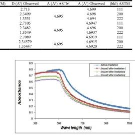
Fig.(2) shows the variation of absorbance (A) as a function of wavelength range (300 – 1000) nm for CdO thin films before and after irradiation, from this figure we can notice that the absorbance values decreased generally as the wave length increases and has low values in the NIR region, we can also observe that these films exhibit an absorption edge and the absorption edge shifts to lower wavelength after irradiation. It is clear from this figure that the value of the absorbance of CdO thin films decreased with increase their radiation time for all values of the wavelength due to improvement of the crystallinity in the films after irradiation leads to growth small grain and decrease grain boundaries; it yields to decrease the absorbance values. Also we can see a strong absorption at wavelength range of (300-500) nm, which is made Cadmium Oxide films suitable for solar cell. The transmittance (T) versus wavelength of CdO thin films before and after irradiation is shown in Fig(3), we can see from this figure that the transmittance value increase with increase irradiation time. Also we can see from this figure the transmittance values increase with increase wavelength and have high values in the NIR region, all samples demonstrate (20-80) % transmittance at wavelengths longer than 500 nm which makes these films
[image:3.595.45.307.85.359.2]Figure 2. The variation of absorbance versus wavelength for cadmium oxide thin films
Figure 3. The variation of transmittance versus wavelength for cadmiumoxide thin films
suitable for solar energy collection. The shift of absorbance and transmittance due to the fact that these are related to the
changes in the films characteristics (Dakhel et al., 2003). The
variation of the absorption coefficient values (α) of CdO films as a function of photon energy before and after irradiation were calculated from equation (7) and shown in Fig (4).We can notice from this figure that all the films have high values
of absorption coefficient (α > 104 cm-1) this means that the
direct transition is possible occurs. This result is in agreement
with refs (Majid H. Hassouni et al., 2013 and Mahaboob
Beevia et al., 2010). Itis clear from this figure thatthe
absorption coefficient values decrease with irradiation time within the whole range of the spectrum and shifts toward higher energy. This behavior may be due to the changes in crystal structure of these films after irradiation, the absorption is not attributed to the free carriers only, but to impurities or Table 1. XRD results of CdO thin films before and after irradiation
State 2 θ (ASTM) 2 θ Observed D (Aº) (ASTM) D (Aº) Observed A (Aº) ASTM A (Aº) Observed (hkl) ASTM
Before irradiation
33.00 38.283 69.284
32.98 38.27 69.28
2.7120 2.3490 1.3550
2.713 2.3499
1.3551 4.695
4.699 4.698 4.694
111 200 222
after irradiation (2houre)
33.00 38.283 69.284
33.02 38.3 69.29
2.7120 2.3490 1.3550
2.7105 2.3482
1.3549 4.695
4.6947 4.696 4.6937
111 200 222
after irradiation (6houre)
33.00 38.283 69.284
33.04 38.34 69.32
2.7120 2.3490 1.3550
2.7089 2.34579
1.35447 4.695
4.6919 4.6915 4.6920
111 200 222
[image:3.595.313.556.388.535.2] [image:3.595.44.280.431.474.2]localized electronic states. We plot (α hν)2 versus photon energy (hν) to find the type of the optical transition for (CdO) films before and after irradiation, which describes the allowed direct transition as shown in Fig.(5) and calculated the optical
energy gap (Egopt) values from Tauc equation (8)by select the
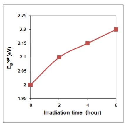
optimum linear part, which determined by the extrapolation of the portion at (α =0). It is clear from Fig. (6) and Table (3) the optical energy gap increased from (2eV) to (2.2eV) when the irradiation time increased. This behavior can be attributed to the decrease of the density of localize states in the Eg after irradiation which caused the energy gap seems large as well as
the reduction in the number of defects in films and the increases in stoichiometric composition, might also lead to the
increase in the optical band gap. The value of the optical
energy gap is agreed with refs (Mahaboob Beevia et al., 2010
[image:4.595.325.540.51.261.2]and Mohamed and Mahmoud Ali, 2008). It can be seen from the Figure (7) the variation of the refractive index values (n) versus wave lengths for (CdO) films before and after irradiation, which calculated from equation (10). It is obvious from result that the refractive index values increases with increasing photon energy followed decrease these value at higher photon energy.
Figure 4. Absorption coefficient behavior as a function of photon energy for cadmium oxide thin films
Figure 5. Variation (α hν)2 & photon energy for cadmium oxide thin films
[image:4.595.41.287.317.486.2]Figure 6. Optical energy gap as a function of Irradiation time for cadmium oxide films
[image:4.595.306.560.327.587.2]Table 3. The optical constant of CdO thin films before and after irradiation
Figure 7. Variation refractive index & photon energy for cadmium oxide thin films
At lower photon energy refractive index values decrease with increasing irradiation time while at higher photon energy after 1.9eV showed an opposite trend these values increases with increasing irradiation time, this behavior may be due to change in the films structure after irradiation. We can notice all samples have a peak refractive index which increase from (1.88 to 2.58) after irradiation and this peak shift to higher photon energy. Fig. (8) shows a plot of the extinction coefficient (K) versus photon energy for CdO thin films as a function of irradiation time, we can notice from this figure that the extinction coefficient behavior nearly similar for all the
State Eg
opt
(eV)
Optical constant at λ =550 nm α x 104
cm-1 n k ε1 ε2
Before
irradiation 2 4.675 1.889 0.2047 3.5269 0.7735
after irradiation
(2houre) 2.1 3.497 2.433 0.1531 5.9007 0.7455
after irradiation
(4houre) 2.15 3.1978 2.526 0.1400 6.3650 0.7076
after irradiation
[image:4.595.53.277.524.723.2]range of the wavelength spectrum to that of the absorption coefficients, this means the extinction coefficient values decrease with irradiation time within the whole range of the spectrum for the same reasons as we mentioned before and have peak shifts toward higher energy. The variation of the
real (ε1) and imaginary (ε2) parts of the dielectric constant
[image:5.595.43.285.172.309.2]values as a function of photon energy for CdO thin films before and after irradiation was seen in Figures (9), (10) respectively.
Figure 8. Variation extinction coefficient & photon energy for cadmium oxide thin films
[image:5.595.310.555.214.356.2]Figure 9. Variation real part of the dielectric constant & photon energy for cadmium oxide thin films
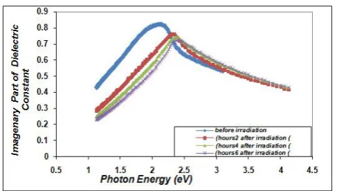
Figure 10. Variation imaginary part of the dielectric constant& photon energy for cadmium oxide thin films
From this figure we can deduce that the values of the real part are higher than those of the imaginary part, the real part of the dielectric constant behavior nearly similar for all the range of the wavelength spectrum to that of the refractive index because of the real part depends mainly on refractive index according
[image:5.595.42.289.347.491.2]to the equation (13), while the imaginary part depend on the extinction coefficient values which are related to the variation of absorption coefficient, we can see from Fig.(10) the imaginary part value decrease with increasing irradiation time at lower photon energy followed increase this values with increasing irradiation time at higher photon energy and the peak shift tohigher photon energy. This behavior is due to the imaginary part is directly related to the density of states within the forbidden gap of semiconductor materials (Mohamed and Mahmoud Ali, 2008). Some of the optical constants values are shown in Table (3). The variation of optical conductivity as a function of photon energy of CdO films before and after irradiation is shown in Fig.(11).
Figure 11. Variation optical conductivity & photon energy for cadmium oxide thin films
We can notice from this figure that the optical conductivity value decreases after irradiated with gamma ray at lower photon energy followed increase this values with increasing irradiation time at higher photon energy. This behavior is due to the optical conductivity value depends mainly on refractive index and absorption coefficients according to the equation (15). The value of the optical conductivity is a good agreement
with refs. (Majid H. Hassouni et al., 2013).
Conclusion
The present study determines the effect of Gamma –Ray irradiation on the structural and optical properties of CdO films.XRD pattern confirms the formation of CdO phase with preferential orientation along (111) plane. Structural analysis results demonstrate that increase the degree of crystallinity and grain size as we exposed the samples to Gamma –Ray. The Optical studies carried out on the films reveal that the absorbance values decrease while the transmittance values increases after irradiation, the average transmittance is more than 70% for wavelengths in the (500–1100) nm range, indicating these films have high transmittance in the NIR region, which makes it suitable for solar energy collection. It also shows that all films prepared before and after irradiation
have high values of absorption coefficient (α > 104 cm-1) and
band gap increases with increase irradiation time. The values of all optical constant (absorption coefficient, refractive index, extinction coefficient, dielectric constant, and optical conductivity) affected after irradiated with gamma ray.
[image:5.595.42.286.527.665.2]REFERENCES
Aksoy, S., Y. Caglar, S. Ilican, M. Caglar, 2009. "Effect of heat treatment on physical properties of CdO films
deposited by sol-gel method, "Int. J. Hydrogen Energy",
34, 5191.
Ali, H., H. Mohamed, M. Wakkad, M. Hasaneen, 2009. Optical and Electrical Properties of Tin-Doped Cadmium Oxide Films Prepared by Electron Beam Technique,
"J. Appl. Phys.", 48 ,041101.
Amutha, S., R. Chandiramouli and B.G. Jeyaprakash, 2012. Microstructural and electrical properties of Mn doped nano structured CdO, "Microstructural and Sciences", 12, 1641-1645.
Blackmore, "Solid state physics", Philadelpia and Tokyo 1974. Calnan, S., Tiwari, A.N. 2010. High mobility transparent
conducting oxides for thin film solar cells, "Thin Solid
Films", 5181839-1849.
Dakhel, A.A. 2013. Germanium doping to improve carrier
mobility in CdO films, "Advances in Opto Electronics",
804646-804652.
Dakhel, A.A; Henari, F.Z. 2003. Optical characterization of
thermally evaporated thin cdo films, "Crystal Research
and Technology", 38, 11, 979-985.
Gupta, R., K. Ghosh, R. Patel, S. Mishra, P. Kahol, 2008. "Structural, optical and electrical properties of In doped
CdO thin films for optoelectronic applications","Mater.
Lett." 62, 4103.
JCPDS, 1997. International Center for Diffraction Data,
ASTM data files 5-64 card No. 05-0640.
Kasap S.O., 2002. ”Principles of Electronic Materials and Devices”, 2nd edition, Mc Graw Hill.
Khalil Arshak, Olga Korostynska, 2006. Gamma radiation
sensors arrays based on metal oxide thick films , "Sensor
Review", 26 Iss: 1, pp.70 - 75
Mahaboob Beevia, M., M. Anusuyab, V. Saravananc, 2010. Characterization of CdO Thin Films Prepared By SILAR
Deposition Technique, "International Journal of Chemical
Engineering and Applications", 1, 2, 151-154.
Majid H. Hassouni, Khudheir A. Mishjil, Sami S. Chiad, Nadir F. Habubi, 2013, Effect of Gamma Irradiation on the Optical Properties of Mg doped CdO Thin films deposited
by Spray Pyrolysis, "International Letters of Chemistry,
Physics and Astronomy", 11, 26-37.
Mane, R.S., H.M. Pathan, C.D. Lokhande and S.H. Han, 2006. An effective use of nano crystalline CdO thin films in dye-sensitized solar cells, "Solar Energy", 80, pp 185-190. Mohamed, H.A.; Mahmoud Ali, H., 2008. Characterization of /TO/cdo /glass thin films evaporated by electron beam
technique, "Sci. Technol. Adv. Mater.", 9, 025016-025025.
Pankove, J. I. “Optical processes in semiconductors”, Dover
Publications, Inc. New York, 1975, 91.
Perumal, P., A. Gowri. Santiyagu, Adaikalamand Jin-Koo Rhee, 2012. Influence of deposition time on the microstructure and transport properties of cdo thin films
prepared by chemical bath deposition, "JSEMAT.", 2, 2,
71-75.
Saha, B., R. Thapa, K. Chattopadhyay, 2008. Wide range tuning of electrical conductivity of RF sputtered CdO thin
films through oxygen partial pressure variation, "Sol.
Energy Mater. Sol. Cells", 92, 1077.
Sinatirajah, P. 2008. Formation of CdO films from chemically
deposited Cd(OH)2films as a precursor, "Applied Surface
Science", 254, 13, 3813-3818.
Suryanarayana, C. and Norton, M.G., "X-ray diffraction, a practical approach", Plenum Press. New York 1998. Taus, J. 1974. “Amorphous and Liquid Semiconductor”,
Plenums Press. New York and London.
Usharani, K. Balu, A. Shanmugavel and G. Suganya, 2013. Transparent conducting cdo thin films fabricated by low cost simplified spray technique using perfume atomizer, "IJSRR.", 2, 3, 53-68.
Viswanath, Aishwarya, N. Nirmmala, Jeyaprakash, and Chandiramouli, 2012. Preparation and characterization of highly conducting and optically transparent fluorine doped
CdO thin films, "Journal of Applied Sciences", 12, Issue
16,p1641 .
William, Callister D., J 2003. ”Materials Science&
Engineering. An Introduction 6th edition, John Wiley Sons
Inc, p.96.
Zaien, M., N.M. Ahmed, and Z. Hassan, 2013. Structural and optical properties of nanocrystalline CdO thin film growth
by solid-vapor deposition, "Advanced Materials
Research", 620, pp241-245.