Dielectrics and Semiconductors
for Thin Film Transistor Applications
Dimitrios Afouxenidis
MSc Materials Physics and TechnologyA thesis submitted in partial fulfilments for the degree of
Doctor of Philosophy
Engineering Department, Lancaster University, UK
2
Transparent thin film transistors (TFTs) have been the subject of extensive scientific research over the last couple of decades, for applications in displays and imaging, as their implementation in active-matrix liquid crystal displays backplanes is expected to improve their performance in terms of switching times and stability. To this end, several material systems have emerged as contenders to address this need for a high performance, low power, large-area electronics i.e. thin film silicon, organic semiconductors and metal oxides. The electronic limitations of thin film silicon are well documented, and although organic semiconductors have seen significant improvements in recent years, their persistent low mobility and instability means that they are unlikely to progress beyond niche applications.
This thesis is focused on the investigation of the physical properties of metal oxides and their implementation in TFTs. Metal oxide based TFTs were fabricated by spray pyrolysis, a simple and large-area-compatible deposition technique.
More precisely, the implementation of titanium-aluminate and niobium-aluminate both wide band gap and high-k gate dielectric metal oxides in solution processed ZnO-based TFTs was studied and high performance, low operational voltage devices were fabricated. ZnO-based TFTs employing stoichiometric Al2O3-TiO2 (k~13, Eg~4.5 eV) or Nb2O5-Al2O3 (k~13.5, Eg~5.1 eV) as gate dielectric exhibited low leakage currents, high on-off current modulation ratios, high field-effect mobilities and low subthreshold voltage swings.
3
I declare that this thesis is my own work and has not been submitted in substantially the same form for the award of a higher degree elsewhere
Dimitrios Afouxenidis
Date:...Monday, 1 October 2018...
4 First and foremost, Ι would like to thank my academic supervisor, Dr George
Adamopoulos, for his unconditional support, constructive criticism and academic guidance throughout the years. Besides great scientist and source of inspiration, I consider him a good friend as well.
I would like to thank Prof Anthony Krier and Prof Claudio Paoloni, for their valuable feedbacks during my research. I would like to express my acknowledgments to Prof Oleg Kolosov and his research group members, for familiarising me with the atomic force microscopy. I would also like to thank the senior lab technician, Mr. Peter Jones, for always having time for me; familiarising me with experimental equipment, answering my queries and helping me to tackle technical problems during experiments.
To that point, I should express my deeply acknowledgements to my friends and colleagues for their help, for inspiring me, and for all the good time we had together; Dr George Polymeris, Dr Lefteris Danos, Dr Emmanouil Papaioannou, Dr Ioannis Tsitsimpelis, Dr Eleftherios Kastis, Dr Anna Κarapiperi, Dr Angelo Greco, Tilly Alton,
Mazran Esro, Mohamed Milad, Armin Yousefi Kanani, Chiemela Victor Amaechi, Ryan Smith, Finn Redman, Gareth Ellis, Apostolis Akritidis, Nikolaos Gkountas, Kostas Tarpanis, Vassiliki Markoulaki, Epaminondas Patiris, Stavroula Lappa, Vasileios
Mantaras, Athina Κommata, Sophia Anastasia Rattan and Zoi Kalou.
5
6
Table of Contents
Abstract ... 2
Declaration ... 3
Acknowledgments ... 4
List of Figures ... 10
List of Tables ... 18
1. Introduction ... 20
1.1 Functional Metal Oxides for Electronic Devices ... 21
1.2 Deposition Techniques: A Brief Overview ... 27
1.2.1 Vacuum Based Deposition Techniques ... 27
1.2.2 Solution Based Deposition Techniques ... 29
1.3 Thesis Outline ... 31
1.4 References ... 32
2. Solution Processed Metal Oxides: An Overview ... 39
2.1 Solution Processed Transparent Oxide (Semi)Conductors ... 40
2.1.1 Binary Oxides ... 40
2.1.2 Multicomponent Oxides ... 49
2.2 Solution Processed Metal Oxide Dielectrics ... 68
2.2.1 Low-k Dielectrics ... 68
2.2.2 High-k Dielectrics ... 68
2.3 References ... 79
3. Theory and Operational Characteristics ... 99
3.1 Introduction ... 100
3.2 MIM Devices ... 101
3.2.1 Impedance Characteristics ... 103
3.2.2 Leakage Current and Conduction Mechanisms ... 107
3.3 Metal Oxide Semiconductor (MOS) ... 113
3.3.1 Accumulation ... 114
3.3.2 Depletion ... 115
3.3.3 Inversion ... 116
7
3.4.1 TFT Operating Characteristics ... 119
3.5 References ... 123
4. Experimental Methods ... 128
4.1 Introduction ... 129
4.2 Deposition Techniques ... 129
4.2.1 Thermo-Chemical Spray Coating ... 129
4.2.2 Thermal Evaporation ... 131
4.3 Characterisation techniques ... 132
4.3.1 Simultaneous thermal analysis (STA) ... 133
4.3.2 X-Ray Diffraction (XRD) ... 134
4.3.3 Atomic Force Microscopy (AFM) ... 135
4.3.4 Ultraviolet-Visible-near IR absorption spectroscopy (UV-Vis-NIR) ... 136
4.3.5 Fourier Transformed Infrared Spectroscopy (FT-IR) ... 138
4.3.6 Ellispometry ... 139
4.3.7 Impedance spectroscopy ... 140
4.3.8 Current Voltage Measurements ... 141
4.4 References ... 143
5. Aluminum Titanate Ti1-xAl2xOy Thin Films ... 147
5.1 Introduction ... 148
5.2 Experimental ... 150
5.2.1 Precursor Solution Chemistry ... 150
5.2.2 Device Fabrication ... 151
5.2.3 Thin Film & Device Characterisation Techniques ... 152
5.3 Results and Discussion ... 153
5.3.1 Precursor thermal properties ... 153
5.3.2 X-Ray Diffraction (XRD) ... 155
5.3.3 Atomic Force Microscopy (AFM) ... 156
5.3.4 UV-Vis-NIR Spectroscopy ... 157
5.3.5 Spectroscopic Ellipsometry ... 159
5.3.6 Impedance Spectroscopy ... 161
5.3.7 I-V characteristics and leakage currents ... 163
8
5.4 Conclusions ... 168
5.5 References ... 169
6. Niobium Aluminate Nb1-xAlxOy Thin Films ... 174
6.1 Introduction ... 175
6.2 Experimental ... 176
6.2.1 Precursor and Solutions ... 176
6.2.2 Device Fabrication ... 177
6.2.3 Thin Film & Device Characterisation Techniques ... 178
6.3 Results and Discussion ... 179
6.3.1 Precursor thermal properties ... 179
6.3.2 UV-Vis-NIR Spectroscopy ... 180
6.3.3 FTIR Spectroscopy ... 182
6.3.4 X-Ray Diffraction (XRD) ... 183
6.3.5 Atomic Force Microscopy (AFM) ... 184
6.3.6 Impedance Spectroscopy ... 185
6.3.7 Leakage Currents ... 187
6.3.8 Field effect measurements ... 195
6.4 Summary ... 199
6.5 References ... 200
7. Solution Processed Crystalline Indium Zinc Oxide (c-IZO) for High Performance Thin Film Transistors ... 208
7.1 Introduction ... 209
7.2 Experimental ... 214
7.2.1 Precursor Solution Chemistry ... 214
7.2.2 Device Fabrication ... 214
7.2.3 Thin Film & Device Characterisation Techniques ... 215
7.3 Results ... 216
7.3.1 Thermal Analysis of Precursor Compounds ... 216
7.3.2 Solution Processed Indium Oxide (In2O3) ... 218
7.3.3 Solution Processed Indium Zinc Oxide (IZO) ... 224
7.4 Summary ... 240
9
7.6 Appendix ... 251
8. High-Performance TFTs based on Indium Zinc Oxide (c-IZO:X) TFTs ... 252
8.1 Introduction ... 253
8.2 Experimental ... 254
8.2.1 Precursor Solution Chemistry ... 254
8.2.2 Device Fabrication ... 255
8.2.3 Thin Film & Device Characterisation Techniques ... 255
8.3 Results ... 255
8.3.1 Thermal Analysis of Precursor Compounds ... 255
8.3.2 Optical & structural properties of c-IZO:X thin films ... 258
8.3.3 Field effect measurements ... 271
8.3.4 Detailed study of IZO:Y. ... 277
8.4 Summary & Discussion ... 286
8.5 References ... 288
9. Conclusions and Further Work ... 292
9.1 Conclusions ... 293
10
List of Figures
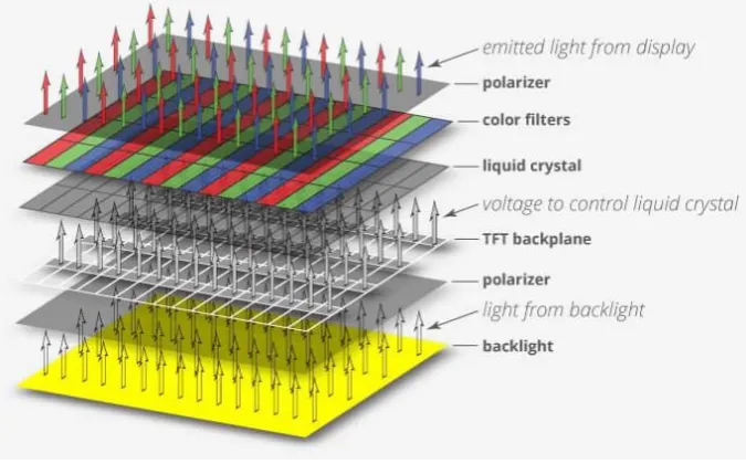
Figure 1-1: Schematic design of a LCD. (Reproduced from) ... 22 Figure 1-2: Schematic orbital drawings for the carrier transport paths (that is,
conduction band bottoms) in crystalline and amorphous semiconductors, reproduced from [10]. ... 25 Figure 2-1: Side and top view of hexagonal wurtzite crystal structure of ZnO, after [2] ... 41 Figure 2-2: Band structure of hexagonal wurtzite ZnO obtained from density-functional
theory calculations (DFT), after [3]. ... 42 Figure 2-3: Crystal structure of cubic (bixbyite) In2O3, after [26]. ... 45 Figure 2-4: Band structure of In2O3, after [31]. ... 46 Figure 2-5: The mobility and hysteresis of solution deposited IZO TFTs annealed at 550
oC by Banger et al. [70] ... 50 Figure 2-6: Variation of band gap and dielectric constant for various oxides,
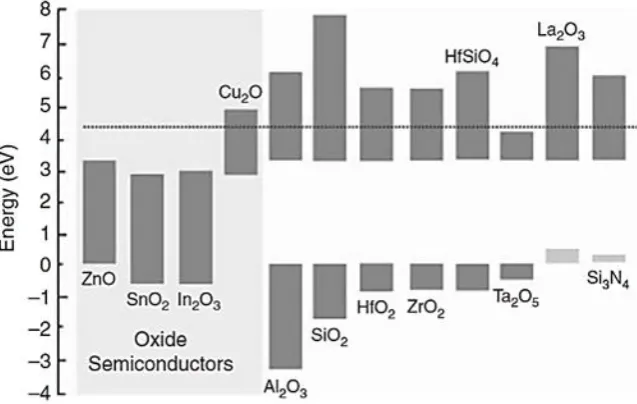
reproduced from [194]. ... 69 Figure 2-7: Calculated band offset of some dielectrics. The values are normalised to
the VBM of ZnO. The thinner line indicates the minimum of 1 eV for CBO. Reproduced from [196] ... 70 Figure 3-1: Metal-insulator-metal (MIM) structure used to assess the properties of the
insulator. ... 101 Figure 3-2: Equivalent circuit of a MIM capacitor. ... 102 Figure 3-3: Impedance vector plane representation. ... 103 Figure 3-4: Frequency response of the equivalent circuit (inset) used to describe
impedance characteristics of a MIM device. ... 105 Figure 3-5: Frequency dependence of the real and imaginary parts of the dielectric
constant, reproduced from. ... 106 Figure 3-6: Classification of conduction mechanisms in dielectric films reproduced
from [16] ... 107 Figure 3-7: Schematic energy-band diagram of Schottky emission in a MIM structure. ... 108 Figure 3-8: Schematic energy-band diagram of Fowler-Nordheim tunnelling in a MIM
structure. ... 110 Figure 3-9: Schematic energy-band diagram of direct tunnelling in MIM structure. 111 Figure 3-10: Schematic energy-band diagram of Poole-Frenkel (PF) emission in MIM
structure. ... 112 Figure 3-11: Typical metal-oxide-semiconductor field effect transistor (MOSFET)
11
Figure 3-12: Energy band diagram for ideal MOS capacitor employing n-type semiconductor at equilibrium (Vapp=0). (1) qφm: φm is the metal work function, (2) qχi: χi is the electron affinity of the insulator, (3) qχ: χ is the electron affinity of the semiconductor, (4) Eg/2: Eg is the band gap of the semiconductor, (5) qφn: φn is the Fermi potential with respect to conduction band edge, (6) qψBn: ψBn is the Fermi potential with respect to midgap edge. ... 114 Figure 3-13: Schematic energy-band diagram MOS capacitor employing n-type
semiconductor under positive voltage bias (Vapp>0). ... 115 Figure 3-14: Schematic energy-band diagram MOS capacitor employing n-type
semiconductor under small negative voltage bias (Vapp<0). ... 116 Figure 3-15: Schematic energy-band diagram MOS capacitor employing n-type
semiconductor under high negative voltage bias (Vg=Vapp<<0)... 117 Figure 3-16:Family tree of Field-Effect Transistors (FETs). Reproduced from [10] .. 118 Figure 3-17: Schematics showing some of the most conventional TFT structures,
according to the position of the gate electrode and the distribution of the electrodes relative to the semiconductor, reproduced from [40]. ... 118 Figure 3-18: Schematic of a thin-film transistor showing the source, drain and gate
contacts, dielectric layer and semiconductor with a graphic representation of the charge accumulation and depletion regions. The device is shown in the saturation regime where VD > VG– VT, reproduced from[41] ... 119 Figure 3-19: Typical a) output and b) transfer characteristics of a n-type oxide TFT,
reproduced from[40] ... 121 Figure 4-1: Schematic diagram of spray pyrolysis equipment configuration, reproduced
from [6]. ... 130 Figure 4-2: Schematic of evaporation system used to deposit metallic contacts. .... 132 Figure 4-3: Schematic design of x-ray diffraction from a periodic atom structure. .. 134 Figure 4-4: Schematic representation of an atomic force microscope setup. ... 136 Figure 4-5:Tauc plot and linear fit for analysis of the Tauc-gap. ... 137 Figure 4-6: Schematic of the operational principles of a UV-Vis spectrophotometer. ... 138 Figure 4-7: Schematic of an FT-IR experimental setup. ... 139 Figure 4-8: Single wavelength ellipsometer setup... 140 Figure 5-1:(a) MIM capacitor and (b) Bottom gate-top contact (BG-TC) ZnO-based TFT
structures used in this study, implementing Ti1-xAl2xOy thin film dielectric. ... 152 Figure 5-2: TGA and DSC data of aluminium (III) chloride powder. TGA and DSC
12
Figure 5-3: TGA and DSC data of titanium (IV) butoxide. TGA and DSC measurements conducted under nitrogen at a scan rate of 10K/min. ... 154 Figure 5-4: GIXRD patterns of selected Ti1-xAl2xOy films deposited by spray pyrolysis on
c-Si substrates. ... 155 Figure 5-5: AFM topography images (RMS roughness inset) of spray deposited Al2O3,
stoichiometric Al2TiOy, and (c) TiO2 films on silicon substrate. ... 156 Figure 5-6: Tauc plots of selected Ti1-xAl2xOy films as function of the
[Ti4+]/([Ti4+]+2[Al3+]) ratio. ... 157 Figure 5-7: Optical band gap of Ti1-xAl2xOy thin films as a function of the
[Ti4+]/([Ti4+]+2[Al3+]) ratio. The solid line is a guide to the eye. ... 158 Figure 5-8: Urbach tail energy (Eu) as a function of the [Ti4+]/([Ti4+]+2[Al3+]) ratio. The
solid line guides the eye. ... 159 Figure 5-9: Schottky barrier pinning factor S of solution processed (SP) Al2O3, TiO2, and
stoichiometric in the solution dielectrics as well as a wide range of dielectrics grown by vacuum-based deposition techniques as well as solutions. ... 161 Figure 5-10: Static dielectric constant (k) dispersions of selected Ti1-xAl2xOy films
deposited by spray pyrolysis. ... 162 Figure 5-11: Dielectric constant (estimated at 10 kHz) of Ti1-xAl2xOy films as a function
of the [Ti4+]/([Ti4+]+2[Al3+]) ratio. The solid line guides the eye. ... 162 Figure 5-12: Static dielectric constant versus band gap of Ti1-xAl2xOy gate dielectrics
deposited by spray pyrolysis. The solid line is a guide to the eye. ... 163 Figure 5-13: Current-Voltage characteristics of selected Ti1-xAl2xOy spray deposited
dielectrics with different [Ti4+]/([Ti4+]+2[Al3+]) ratio. ... 164 Figure 5-14: Leakage current density of solution processed Ti1-xAl2xOy gate dielectrics
at 2 and 3 MV/cm as a function of the [Ti4+]/([Ti4+]+2[Al3+]) ratio. The solid lines guide the eye. ... 164 Figure 5-15: a) Transfer and b) output characteristics of ZnO-based TFTs employing
spray coated Al2O3 gate dielectric. ... 166 Figure 5-16: a) Transfer and b) output characteristics of ZnO-based TFTs employing Ti 1-xAl2xOy gate dielectric ([Ti4+]/([Ti4+]+2[Al3+])~45%). ... 166 Figure 5-17: Band diagrams of ZnO, Al2O3 and TiO2 and estimated conduction and
valence band offsets on ZnO. ... 167 Figure 6-1: (a) MIM capacitor and (b) Bottom gate-top contact (BG-TC) ZnO-based TFT
structures used in this study, implementing Nb1-xAlxOy thin film dielectric. ... 178 Figure 6-2: TGA and DSC data of niobium (V) chloride. TGA and DSC measurements
conducted under nitrogen at a scan rate of 10K/min ... 179 Figure 6-3: Tauc plots of selected Nb1-xAlxOy films of different [Nb5+]/([Nb5+]+[Al3+])
13
Figure 6-4: Optical band gap of Nb1-xAlxOy thin films as a function of the
[Nb5+]/([Nb5+]+[Al3+]) ratio. The solid line is a guide to the eye. ... 181
Figure 6-5: Urbach tail energy (Eu) as a function of the [Nb5+]/([Nb5+]+[Al3+]) ratio. The solid line guides the eye. ... 181
Figure 6-6: FTIR spectra of selected Nb1-xAlxOy films and NbCl5 and AlCl3 precursors deposited on KBr substrates. ... 182
Figure 6-7: GIXRD patterns of selected Nb1-xAlxOy films of different [Nb5+]/([Nb5+]+[Al3+]) ratios. ... 183
Figure 6-8: Friction and topography (inset) images (RMS roughness inset) of solution-processed AlOx, stoichiometric Nb0.5Al0.5Oy, and (c) NbOx films on silicon substrates. ... 184
Figure 6-9: Static dielectric constant (k) dispersion of selected Nb1-xAlxOy films in the frequency range of 1 kHz-10 MHz ... 185
Figure 6-10: Dielectric constant of Nb1-xAlxOy films as a function of the [Nb5+]/([Nb5+]+[Al3+]) ratio. The solid line is a guide to the eye. ... 186
Figure 6-11: Static dielectric constant (k) vs band gap for Nb1-xAlxOy dielectrics grown by spray pyrolysis. The solid line is a guide to the eye. ... 186
Figure 6-12: Leakage current density-electric field characteristics of selected Nb1-xAlxOy spray deposited dielectrics as a function of the [Nb5+]/([Nb5+]+[Al3+]) atomic ratio (in the solution). ... 187
Figure 6-13: Leakage current density of solution processed Nb1-xAlxOy gate dielectrics at 0.5 and 1 MV/cm as a function of the [Nb5+]/([Nb5+]+[Al3+]) atomic ratio in the solutions. The solid lines are guides to the eye. ... 188
Figure 6-14: Schottky emission (SE) plots of selected Nb1-xAlxOy films. ... 189
Figure 6-15: Fowler-Nordheim (FN) plots of selected Nb1-xAlxOy films. ... 190
Figure 6-16: Poole-Frenkel (PF) plots of selected Nb1-xAlxOy films. ... 191
Figure 6-17: Schematic energy-band diagram of Schottky emission in a MIM structure. ... 192
Figure 6-18: a) Electron effective mass in the Nb1-xAlxOy and b) barrier height at the Au/Nb1-xAlxOy interface as a function of the [Al3+]/([Nb5+]+[Al3+]) ratio. The lines are guides to the eye. ... 193
Figure 6-19: Energy band diagrams of selected Nb1-xAlxOy films. The conduction bands (black solid lines) are presented in respect to gold’s fermi energy (EF). The calculated effective masses included as well. ... 193
Figure 6-20: Fowler-Norheim plot of the stoichiometric Nb1-xAlxOy film. ... 194
Figure 6-21: a) Transfer and b) output characteristics of ZnO-based TFTs employing spray coated AlOy gate dielectric. ... 195
14
Figure 6-23: Field effect mobility (left Y-axis) and on/off current modulation ratio (right Y-axis) of ZnO-based TFTs employing spray coated Nb1-xAlxOy gate dielectrics. ... 197 Figure 6-24: Conduction band offsets (ΔΕc) of spray coated Nb1-xAlxOy gate dielectrics
with ZnO. ... 198 Figure 6-25: Band diagrams of conduction band offsets for dielectric (a) without gap
states, (b) with gap states close to conduction band minimum. (Ec1: conduction band minimum of zinc oxide, Ev1: valence band maximum of ZnO, EF1: Fermi level of ZnO, Ec2: Conduction band minimum of a dielectric, EF2(=Eg/2): Fermi level of dielectric assuming no gap states in its band gap, E’
F2: Fermi level of dielectric assuming gap states in its band gap, ΔΕF2: the transposition (in eV) of Fermi level from midgap, ΔEc: conduction band offset for dielectrics without gap states, ΔE’c=ΔΕc-ΔEF2: conduction band offset for dielectrics with gap states). ... 199 Figure 7-1: Schematic orbital contours for charge transport pathways in the
conduction band of crystalline a) covalent semiconductor, b) metal oxide semiconductor, disorder c) covalent semiconductor and d) metal oxide semiconductor. ... 210 Figure 7-2: (a) Single-crystal InGaZnO4, (b) plane, and (c) cross-section transmission
electron microscopy (TEM) images of a c-axis-aligned indium gallium zinc oxide (CAAC IGZO) thin film (In:Ga:Zn=1:1:1). The InO2 layer has a compositional ratio of In:O=1:2 and the (Ga,Zn)O layer has a compositional ratio of Ga:Zn:O=0.5:0.5:1. In: Indium. Ga: Gallium. Zn: Zinc. O: Oxygen. Reprinted from [49] ... 212 Figure 7-3: TFT fabrication routine followed in this study: a) ultrasonically clean
glass/ITO substrate, b) heated glass/ITO substrates were spray coated with the Al2O3 precursor solution, c) deposition of IZO semiconducting channel by spray pyrolysis and d) deposition of source and drain electrodes by thermal evaporation. ... 215 Figure 7-4: TGA (black line) and weight loss rate (red line) and DSC (right Y axis) data
of 30 mg indium (III) chloride powder. TGA and DSC measurements conducted under nitrogen at a heating rate of 10 K/min... 216 Figure 7-5: TGA (black line) and weight loss rate (red line) and DSC (right Y axis) data
of 15 mg zinc acetate dihydrate powder. TGA and DSC measurements conducted under nitrogen at a heating rate of 10 K/min... 217 Figure 7-6: Tauc plots of spray deposited In2O3 films, for different deposition
temperatures. ... 218 Figure 7-7: Variation of band gap (left Y axis) and Urbach tail energy (right Y axis) with
deposition temperature of In2O3 films. ... 219 Figure 7-8: FT-IR spectra of spray deposited In2O3 thin films at different substrate
15
Figure 7-10: IDS (left axis) and IDS1/2 (right axis) versus VGS curves of spray deposited In2O3-based TFTs for different In2O3 deposition temperatures (a) 350oC, (b) 400oC, (c) 450oC and (d) 500oC. The channel length (L) and width (W) were 100 and 1000 μm respectively. ... 222 Figure 7-11: Extracted operational characteristics of spray deposited In2O3-based TFTs
for different deposition temperatures. a) threshold voltage, b) off-state current, c) field effect mobility in saturation regime and d) subthreshold swing. (The lines are guides to the eyes) ... 223 Figure 7-12: Optical transmittance of IZO thin films deposited by spray pyrolysis on
fused silica substrates ... 225 Figure 7-13: Tauc Plots of selected IZO spray deposited thin films. ... 226 Figure 7-14: Urbach tail energy Eu (left axis) and optical band gap energy (right axis) of
spray deposited IZO thin films as a function of [Zn2+]/([Zn2+]+[In3+]) in the solution. The lines are guides to the eye. ... 226 Figure 7-15: FTIR spectra of spray deposited IZO films on KBr substrates for different
wavenumber regions. ... 228 Figure 7-16: X-ray diffraction of spray deposited IZO films on Si substrates for different
[Zn2+]/([Zn2+]+[In3+]) ... 229 Figure 7-17: (a) average crystallite size, calculated from (222) diffraction peaks, (b)
interplanar spacing dhkl calculated for (222) plane, (c) lattice parameter a calculated from the (222) diffraction peak and (d) the corresponding lattice volume assuming the cubic bixbyite cubic In2O3 structure. ... 231 Figure 7-18: Representation of In2O3 lattice structure assuming a) Zn2+ interstitials and
b) Zn2+ interstitials and substitutions in In3+ site. ... 232 Figure 7-19: Atomic force images of spray deposited IZO films on Si substrates for
different [In3+]:[Zn2+] ratios. ... 236 Figure 7-20: Transfer characteristics (IDS-VGS), in saturation regime (VDS=20 V), of the
spray deposited IZO thin films for different [In]:[Zn] atomic ratios. (a) Indium rich region, (b) zinc rich region. ... 237 Figure 7-21: (a) off-state current, (b) current modulation, (c) field effect mobility, (d)
subthreshold voltage swing. The lines are guides to the eye. ... 238 Figure 7-22: Transfer (left) and output (right) characteristics of the spray deposited IZO
based thin film transistor possessing a [In3+]:[Zn2+]=6:4 stoichiometry. 240 Figure 7-23: FTIR spectra of IZO thin films and the InCl3 and Zn(O2C2H3)2.2H2O
precursors demonstrating the complete decomposition of the precursors. ... 251 Figure 8-1: TGA (black line) and weight loss rate (red line) and DSC (right Y axis) data
16
Figure 8-2: TGA (black line) and weight loss rate (red line) and DSC (right Y axis) data of 15 mg zirconium (IV) acetylacetonate powder. TGA and DSC measurements conducted under nitrogen flow at a heating rate of 10 K/min. ... 257 Figure 8-3: TGA (black line) and weight loss rate (red line) and DSC (right Y axis) data
of 15 mg gallium (III) chloride powder. TGA and DSC measurements conducted under nitrogen flow at a heating rate of 10 K/min... 258 Figure 8-4: a) Transmittance spectra and b) Tauc plots of the IZO:Ga thin films for
different Ga doping concentration. ... 259 Figure 8-5: Optical band gap and Urbach tail energy of IZO:Ga films as a function of Ga doping levels. Lines are guides to the eye. ... 260 Figure 8-6: FTIR absorption spectra of Ga -doped IZO, at two different spectra regions,
on KBr substrates for thin films of varying Ga doping ratios. ... 261 Figure 8-7: GIXRD diffraction patterns of Ga-doped c-IZO films for varying Ga doping
ratios. ... 262 Figure 8-8: a) Transmittance spectra and b) Tauc plots of the IZO:Y thin films for
different Y doping concentration ... 263 Figure 8-9: Optical band gap and Urbach tail energy of IZO:Y thin films as a function of
Y fraction. Lines are guides to the eye. ... 263 Figure 8-10: GIXRD diffraction patterns of Y-doped c-IZO films for varying Y doping
ratios. ... 264 Figure 8-11: (a) average crystal size and (b) lattice strain calculated from (222) plane
of IZO:Y thin films as a function of Y fraction. The lines are guides to the eye. ... 265 Figure 8-12: a) Transmittance spectra and b) Tauc plots of the IZO:Zr thin films for
different Zr doping concentration ... 266 Figure 8-13: Optical band gap and Urbach tail energy of IZO:Zr thin films as a function
of Zr content. The lines are guides to the eye. ... 267 Figure 8-14: FTIR absorption spectra of Zr-doped IZO on KBr substrates for thin films
of varying Zr doping ratios. ... 267 Figure 8-15: a) Transmittance spectra and b) Tauc plots of the IZO:Nb thin films for
different Nb doping concentration ... 269 Figure 8-16: Optical band gap and Urbach tail energy of IZO:Nb thin films as function
of Nb5+ content. The lines are guides to the eye. ... 269 Figure 8-17: FTIR absorption spectra of Nb-doped IZO on KBr substrates for thin films
of varying Nb doping ratios. ... 270 Figure 8-18: Transfer characteristic of (a) Ga -doped IZO, (b) Y -doped IZO, (c) Zr -doped
IZO, (d) Nb -doped c-IZO thin films with different doping ratios. ... 272 Figure 8-19: Off-state current (Ioff) of c-IZO:X, (X=Ga, Y, Zr, Nb) based TFTs as a function
17
Figure 8-20: Field effect mobility (μ) of c-IZO:X, (X=Ga, Y, Zr, Nb) based TFTs as a function of X content in the films. ... 275 Figure 8-21: Subthreshold slope (SS) of c-IZO:X, (X=Ga, Y, Zr, Nb) based TFTs as a
function of X content in the films. ... 276 Figure 8-22: (a) Tauc plots of selected c-IZO:Y films, (b) optical band gap and Urbach
energy as a function of the [Y3+]/([In3+]+[Zn2+]) atomic ratio. The solid lines are guides to the eye. ... 277 Figure 8-23: GIXRD diffraction patterns of Y-doped c-IZO films with different
[Y3+}/([In3+]+[Zn2+]) ratios. ... 278 Figure 8-24: (a) Average grain size (<d>) and (b) interplanar spacing (dhkl) calculated
from the (222) diffraction peak as a function of [Y3+]:[In3+] atomic ratio (in the solution). ... 279 Figure 8-25: Lattice parameter a for Y-doped c-IZO thin films as a function of
[Y3+]/([In3+]+[Zn2+]) atomic ratio. ... 280 Figure 8-26: Channel formation at grain boundaries and carrier transport pathway
[34]. ... 281 Figure 8-27: AFM (topography and friction) images of selected c-IZO:Y thin films. . 282 Figure 8-28: Field effect mobility of c-IZO:Y based TFTs as a function of
[Y3+]/([In3+]+[Zn2+]) atomic ratio. ... 284 Figure 8-29: Off-state current of c-IZO:Y based TFTs as a function of [Y3+]/([In3+]+[Zn2+])
18
List of Tables
Table 1-1: Thin film deposition techniques. ... 27 Table 2-1: Selected previous work on solution processed ZnO semiconductors based
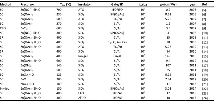
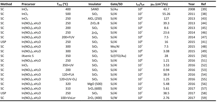
on the number of citations. (SC: spin-coating, SP: spray pyrolysis, CBD: chemical bath deposition, Zn(OAc)2: zinc acetate, ATO: Al2O3/TiO2, superlattice, LAO: lanthanum aluminate, AlTiO: Aluminum titanate, ITO: tin doped indium oxide, Tdep: deposition temperature, tox: gate dielectric thickness, SD: source drain, Ion/Ioff: current modulation, μFE: field effect mobility). ... 43 Table 2-2: Selected previous work on solution processed In2O3 semiconductors based
on the number of citations. (SC: spin-coating, USP: ultrasonic spray pyrolysis, ITO: tin doped indium oxide, Tdep: deposition temperature, SD: source drain, Ion/Ioff: current modulation, μFE: field effect mobility, iXsenic: precursor solution developed by Evonik, FUV: far ultraviolet, FLA: flash lamp annealing, VisLzr: visible laser, UV-O3: Ultraviolet-ozone), SAND: self-assembled nanodielectric. ... 48 Table 2-3: Selected previous work on solution processed multicomponent metal oxide-based semiconductors. (IJP: ink-jet printing, SC: spin-coating, ITO: indium-tin oxide, Tdep: deposition temperature, SD: source drain, Ion/Ioff: current
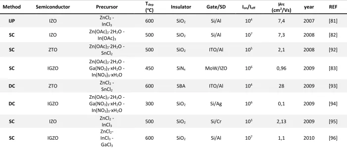
modulation, μFE: field effect mobility, IZO: indium-zinc oxide, ZTO: zinc-tin oxide, IGZO: indium-gallium-zinc oxide, YIZO: yttrium-indium-zinc oxide, LIZO: lanthanum-indium-zinc oxide, ZITO: zinc-indium-tin oxide, MIZO: magnesium-indium-zinc oxide, SrIZO: strontium-indium-zinc oxide, SiIZO: silicon-indium-zinc oxide, ZIZO: zirconium-indium-zinc oxide, GSIZO: gallium-silicon-indium-zinc oxide, LZTO: lanthanum-zinc-tin oxide, L-YIZO: lithium-yttrium-indium-zinc oxide, AIZO: aluminum-indium-zinc oxide, HIZO: hafnium-indium-zinc oxide, GeIZO: germanium-indium-zinc oxide, WIZO: tungsten-indium-zinc oxide, BIZO: borium-indium-zinc oxide) ... 56 Table 2-4 Dielectric constant (k) and band gap (Eg) values of some gate oxides,
reproduced from [202] ... 71 Table 2-5: Literature review of solution processed aluminum oxide gate dielectrics
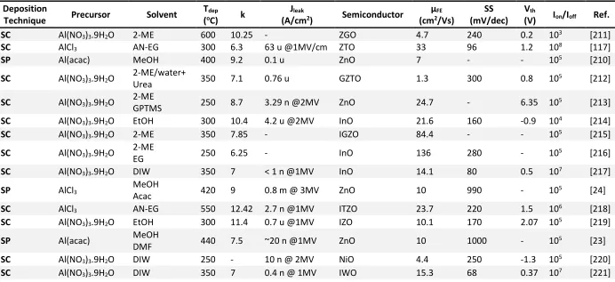
used in various TFTs. (SC: Spin coating, SP: spray pyrolysis, ME: 2-methoxyethanol, AN: acetonitrile, EG: ethyleneglycol, MeOH: methanol, EtOH: ethanol, acac: acetylacetone, DIW: deionised water, DMF: N,N-dimethylformamide, GPTMS: (3-glycidoxy- propyl)trimethoxysilane, ZGO: zinc-gallium oxide, ZTO: zinc-tin oxide, GZTO: gallium-zinc-tin oxide, IGZO: gallium-zinc oxide, ITZO: tin-zinc oxide, IWO: indium-tungsten oxide, IZO: indium-zinc oxide, Tdep: maximum deposition temperature, k: dielectric constant, Jleak: leakage current density, μFE: field-effect mobility, SS: subthreshold slope, VTH: threshold voltage, Ion/Ioff: on-off current ratio). ... 73 Table 2-6: Literature review of solution processed metal aluminate gate dielectrics.
19
acetonitrile, EG: ethyleneglycol, MeOH: methanol, acac: acetylacetone, n-buto: n-butoxide, DIW: deionised water, DMF: N,N-dimethylformamide, IGZO: gallium-zinc oxide, ITZO: tin-zinc oxide, IZO: indium-zinc oxide, Tdep: maximum deposition temperature, k: dielectric constant, Jleak: leakage current density, Eb: dielectric strength, μFE: field-effect mobility, SS: subthreshold slope, VTH: threshold voltage, Ion/Ioff: on-off current ratio, HAO: hafnium aluminate, ZAO: zirconium aluminate, TAO: titanium aluminate, LAO: lanthanum aluminate, *: no available data). .. 78 Table 4-1: Summary of the conduction mechanisms used to assess the conductivity of
thin insulating films. ... 142 Table 7-1: Operational characteristics of spray deposited In2O3 based TFTs, for
different deposition temperatures. ... 222 Table 7-2: Summary of operational characteristics of the spray deposited IZO thin films
20
21
1.1
Functional Metal Oxides for Electronic Devices
Modern transparent electronics require wide band gap conductors, semiconductors and dielectrics which are transparent in the visible range of the electromagnetic spectrum for the fabrication of electronic devices and circuits. These fundamental requirements are fulfilled by metal oxides.
Generally, the term metal-oxide refers to compounds which are formed with metal and oxygen in the form of oxide ion (O2-). Metal oxides constitute an important class of materials due to their ability to demonstrate novel and tunable properties. There are metal oxides that are insulators, semiconductors, conductors or either superconductors. These macroscopic properties strongly depend on their composition.
The most well-studied class of the metal oxides are the transparent conductive oxides (TCOs). Their applications include smart windows applications, flat panel displays (FPDs) and photovoltaic cells. Regarding the usage of TCOs for low emission windows, fluorine doped tin oxide (FTO) has been used for energy efficient windows, due to their low radiative heat loss because of their low thermal emittance [1]. For FPDs, TCOs such as crystalline indium tin oxide (ITO) and amorphous indium zinc oxide (a-IZO) has been used as transparent electrodes. The a-IZO is a relatively new entry in the FPD industry. It is of amorphous structure and can be deposited at room temperature by vacuum-based deposition techniques. TCOs are also a very important class of materials for PV applications [2], [3]. In PV industry ITO has been implemented as the front side electrode in thin film solar cells because of its high conductivity and
transparency at the same time. Because of ITO’s manufacturing cost (indium is scarce
and consequently expensive), alternative indium-free metal oxides have been considered as potential replacements. Fluorine and antimony doped tin oxide (FTO, ATO) have been considered as low-cost alternatives to ITO [4], [5].
22
[image:22.595.146.484.379.589.2]The most interesting field of metal oxides is that of high performance, fully transparent TFTs. The necessity of high performance and highly transparent TFTs has originated from the FPD market. The most common technology in FPD industry is the liquid crystal displays (LCDs). A schematic of a LCD is shown in Figure 1-1. As the light source is located on the back of the TFT backplane, enhanced optical transparency of the TFT would enhance the optical performance of the display. Additionally, metal-oxide based TFTs exhibit higher electron mobility than amorphous silicon (a-Si) which is currently in use, increasing the performance of the devices. Furthermore, the implementation of high-k metal oxide based dielectric materials in the TFT structure as gate dielectrics, could reduce the operational voltage which leads to low power consumption. The low power electronic devices are of particular interest nowadays because of the market interest on portable devices such as high performance and ultra-portable notebooks, tablets and smartphones.
Figure 1-1: Schematic design of a LCD. (Reproduced from1)
For low voltage and high-performance transparent metal oxide based TFTs several metal oxides with different electrical properties have been studied [6]. As metallic like contacts, indium-tin oxide (ITO), indium-zinc oxide (IZO), gallium-zinc oxide (GZO), aluminum-zinc oxide (AZO) are the most well studied metal oxides that
23
they have been implemented in TFT structures acting as gate and source-drain electrodes. A number of high-k, wide band gap metal oxides have been extensively studied as gate dielectrics. Aluminum oxide (Al2O3), hafnium oxide (HfO2), yttrium
oxide (Y2O3), zirconium oxide (ZrO2) are characteristic metal oxides that have been
implemented as gate dielectrics in fully transparent TFTs. Binary metal oxides such as aluminum-titanium oxide (TAO), hafnium-aluminum oxide (HAO), lanthanum-aluminum oxide (LAO) have equally been studied as potential gate dielectrics.
Finally, the most extensively studied field towards high performance TFTs is the field of metal oxides. Metal-oxide based semiconductors are in general degenerated TCOs. Transparent conductive oxides exhibit a free carrier concentration (Nc) in excess of 1020 cm-3 (Nc>1020 cm-3) while, transparent oxide semiconductors (TSOs) are metal oxides possessing a free carrier concentration typically in the range of 1014-1018 cm-3
[7]. Thus, the conductivity of the TSOs can be tuned by using proper setups like field effect transistors, where by applying a voltage to the gate electrode the current flow from source to drain electrode can be controlled.
Zinc oxide (ZnO) is maybe one of the most extensively studied TSO. There is a very high volume of research papers, dealing with the deposition methods of ZnO and how these affect the physical properties of the deposited ZnO thin films. Hoffman et al. in 2003 were prepared a fully transparent ZnO based TFT [8]. They deposited the
ZnO active layer on top of a glass/ITO/ATO stuck via sputtering resulting in a glass/ITO/TAO/ZnO stack. ITO was serving as gate electrode while ATO (alternating layers of Al2O3 and TiO2) was serving as gate dielectric. Finally, ITO was deposited by sputtering through shadow masks acting as source-drain electrodes. The device
exhibited an effective channel mobility of 0.35-0.45 cm2/Vs, a threshold voltage of
10-15 V and a high current on-to-off ratio of about 107.
24
showed impressive operational characteristics such as a field effect mobility of 80
cm2/Vs, a turn on voltage of -0.5 V and an on-off current modulation ratio of 106.
In 2004, Nomura et al. introduced for first time a flexible metal oxide-based thin film transistor, deposited at room temperature by PLD, implementing amorphous IGZO (a-IGZO) as semiconducting layer [10]. In their device Y2O3 was serving as the
gate dielectric while ITO was serving as gate and source-drain electrode.
Nomura’s work opened a whole new era for metal oxide based electronic
devices. Since then extensive studies for amorphous oxide semiconductors (AOSs) were conducted to replace the amorphous hydrogenated silicon (a-Si:H).
AOSs, in contrast to a-Si:H, are not affected by the degree of disorder. In covalent semiconductors such as a-Si:H the carrier transport pathways consist of hybrid 𝑠𝑝3 orbitals. So, the bonds, which are the main carrier transport pathway, in covalent semiconductors are highly sensitive to structural disorder. So, any kind of structural disorder significantly alters the electronic properties of such semiconductors. On the other hand, oxide-based semiconductors, especially for the
transitional metal oxide-based ones with electronic structure of (n-1)d10ns0, (n≥4), the carrier transport pathways are the bottom of conduction band or conduction band minima (CBM). The CBM of most metal oxides consists of spatially spread spherical metal s-type molecular orbitals, 𝑛𝑠 orbitals . In contrast, the maximum of the valence band (VBM) is formed of oxygen 2𝑝 orbitals [11]. Figure 1-2 shows a schematic for the carrier transport paths in crystalline and amorphous semiconductors.
25 Figure 1-2: Schematic orbital drawings for the carrier transport paths (that is, conduction band bottoms) in crystalline and amorphous semiconductors, reproduced from [10].
The majority of reported AOSs are based on the binary systems of indium oxide (In2O3), zinc oxide (ZnO) and tin oxide (SnO2). Such materials satisfy the criterion of
(n-1)d10ns0, (n ≥4), for high performance oxide semiconductors. However, these oxides are of polycrystalline nature. To form amorphous metal oxide semiconductors, blending such binary oxides has been proposed. The combination of indium oxide and the zinc oxide (IZO) results to an amorphous structure, under a particular stoichiometry (0.25<[In]:[Zn]< 0.8), which results in enhanced TFT operational characteristics such as high carrier mobility and low hysteresis [13]. Taking the advantage of its structure, a-IZO exhibits a wide range of conductivity depending on the [In]:[Zn] atomic ratio and the deposition conditions. A number of TFTs have been reported by various research groups based on a-IZO [14]–[20]. Despite the fact that a-IZO based TFTs have been reported, the control of carrier concentration still remains
26
carrier concentration the inclusion of various metal cations such as Ga3+ [10], [21]–
[25], Zr4+ [26]–[29], Hf4+ [30]–[34], Y3+ [35]–[38], La3+ [39], [40], have been studied.
Among these, Ga3+ is the most studied after Nomura’s pioneering work [10]. It has
been reported that metal cations such as Ga3+, could effectively suppress the carrier
concentration down to 𝑁𝑐 < 1017 cm-3, as a result of gallium’s high ionic potential.
Because of the high ionic potential of Ga3+ metal cations, Ga3+ attracts oxygen ions and binds them, suppressing the formation of oxygen vacancies.
Besides the advantages of AOSs, instability issues such as threshold voltage shift (ΔVth) and deterioration of subthreshold voltage swing (ΔSS) under negative (NBS) or positive (PBS) bias, or illumination (NBIS, PBIS) conditions have been reported [6], [41]–[47]. The stability of the TFTs under gate bias and illumination conditions is of significant importance for their implementation in transparent circuit applications. For instance, a shift in threshold voltage could result in an undesirable change of luminance in an OLED pixel resulting in a significant change of the brightness and contrast of the OLED based displays. The origin of such instability issues, is attributed, in general, to charge trapping, defect creation, vacancy ionisation and environmental conditions [12], [48]. Bias stress has been considered as responsible for carrier generation or carrier trapping at the dielectric-semiconductor interface or at the semiconductor itself. Illumination has been found that is responsible for vacancies ionisation resulting in carrier generation shifting the threshold voltage [49].
Different approaches have been followed to tackle the reliability issues of AOSs. Very recently, Yamazaki et al., introduced crystalline IGZO or more precisely c-axis aligned crystalline IGZO (CAAC-IGZO) and they showed that it provides higher reliability than the amorphous counterparts [50]. Besides CAAC-IGZO, nanocrystalline IGZO (nc-IGZO), In-Sn-Zn oxide either as nanocrystalline (nc-ITZO) or c-axis aligned crystalline (CAAC-ITZO) have been considered as channel materials for backplane TFTs in LCD panels [51]. Such materials, developed by Yamazaki’s group exhibit high
27
1.2
Deposition Techniques: A Brief Overview
Metal oxide films have been deposited on various substrates by using a variety of deposition techniques, divided into two main groups, i) vacuum and ii) solution-based deposition ones. Both the techniques show advantages and disadvantages over each other.
In Table 1-1 a summary of the most common used vacuum and solution-based deposition techniques is presented.
Table 1-1: Thin film deposition techniques.
Vacuum Deposition Techniques Solution Deposition Techniques
Thermal Evaporation (TE) Chemical Bath
Electron Beam Evaporation (EBE) Spin Coating
Molecular Beam Epitaxy (MBE) Dip Coating
Sputtering Doctor Blade
Plasma Enhanced-
Chemical Vapour Deposition (PECVD) Spray Pyrolysis
Pulsed Laser Deposition (PLD) Inkjet Printing
Atomic Layer Deposition (ALD)
1.2.1 Vacuum Based Deposition Techniques
Vacuum-based deposition techniques include physical vapour deposition (PVD) as well as chemical vapour deposition (CVD). Physical vapour deposition (PVD) include among others, thermal (TE) and electron beam evaporation (EBE), molecular beam epitaxy (MBE), sputtering and the pulsed layer deposition (PLD). On the other hand, the vacuum-based chemical vapour (CVD) deposition techniques include metal organic chemical vapour deposition (MOCVD), plasma enhanced chemical vapour deposition (PECVD) and atomic layer deposition (ALD).
Deposition of thin films by vacuum-based techniques requires high vacuum
28
(source/target) is either a metal or metal-oxide material which pulverised to ions or vapours and it deposited on the substrate.
In thermal evaporation (TE) or resistance heating technique, the source material is heated by an electrical current through a filament or a resistance heated
boat under high vacuum (<10-5 mbar). The source solid material is turned into vapour which travels in the chamber and is deposited on the substrate to form a thin film. In contrast, in the electron beam evaporation (EBE) instead of a heated filament or a resistance heated boat, the source material is tuned into vapours by high energy electron beam bombardment on the material to be deposited. An electron gun is used to generate the electron beam by thermionic emission of electrons from a filament and the electrons are accelerated by an electric field.
In molecular beam epitaxy (MBE) the thin films are being epitaxial grown. This combines both the physical and chemical vapour deposition methods. The source material is heated to its evaporation point, turns into gaseous form and the beams of atoms or molecules are forwarded toward a heated monocrystalline substrate [54]. In
this technique the crystalline substrate is very important, and the properties of the deposited film strongly depend on it. The deposition rate is low, but the films are of high crystalline quality.
The most widely used technique for thin films deposition is the sputtering. In its simplest configuration, it consists of a vacuum chamber which is filled with an inert gas such as argon and a metallic anode and cathode to produce a glow discharge.
Sputtering is the process that atoms from the target’s surface is physically vaporised
by momentum transfer from bombarding energetic atomic sized particles [55]. There are two common types of sputtering process: direct current (DC) and radio frequency (RF) sputtering.
In plasma enhanced chemical vapour deposition (PECVD) gaseous precursors are used to deposit the requested materials. The gaseous precursors are turned into reactive ions, atoms, molecules by plasma.
29
surface of the source material. The ablated, from a pulsed laser, atoms are deposited on the substrate. PLD is a deposition technique that in general does not require an ultra-high vacuum, as other vacuum-based techniques. A major drawback of PLD is the large area incompatibility [59].
Atomic layer deposition (ALD) is a chemical vapour deposition technique. In ALD two or more gaseous precursors are used sequentially. Firstly, the deposition chamber is vacuumed to remove any kind of unwanted air molecules. The first gaseous chemical is then introduced into the reaction chamber by a carrier gas and it reacts with the substrate to form the first layer of the film. Then the reaction chamber is evacuated again, and the second gaseous precursor is introduced. ALD is a sequential deposition technique. It is a slow deposition technique, but it can run even at lower temperatures.
1.2.2 Solution Based Deposition Techniques
Solution based deposition techniques include among others, the chemical bath deposition, the spin and dip coating technique, the so-called doctor blade technique the spay pyrolysis or spray coating deposition technique and the inkjet printing. Among them, spin coating and spray pyrolysis are the two more frequently used techniques for the deposition of metal oxide films.
The chemical bath deposition (CBD) technique has been extensively used to deposit metal chalcogenide thin films [60]–[62]. Chemical bath deposition requires simple instrumentation; just a hot plate with a magnetic stirrer. In CBD the deposition of the films takes place on a substrate immersed in the precursor solution by chemical reactions. With CBD, a large number of substrates can be coated in a single run with a proper jig design.
30
relatively fair thickness control. The drawback of film thickness control is due to the difficulty to homogeneously wet a substrate [64].
Doctor blade and inkjet printing are both printing techniques that they have been used in the field of thin films. Doctor blade (or tape casting) is a rotogravure printing technique [65]. A blade removes the excess of the solution deposited on the desired substrate. The substrate is heated then to the desired temperature to convert the precursor to the metal oxide. Doctor blade is a deposition technique that is mainly used in the field of organic electronics.
Inkjet printing has been considered as one of the cost-effective direct write techniques for films manufacturing. The use of this technique in electronics manufacturing, where interconnects and other conductive features are required is an area of increasing relevance to the fields of electronics manufacturing, packaging and assembly [66].
Among the widely used solution processed thin film deposition techniques, spin coating is the most popular ones. Spin coating is the technique that a precursor solution is deposited onto a rotating substrate. For the deposition of thin films, the spin coater is accelerated to uniformly spread the solution and let the solvent to be evaporated. The substrate is then heated up to let the solvent be evaporated. This step is repeated several times until the desired film thickness is reached. The thickness of the film depends on several parameters, i.e. the chemistry of the solution, the nature of the substrate, the speed and the time of the spinning process. Finally, to enhance the properties of the as deposited thin film a post deposition annealing at higher temperatures is usually occurred.
31
In this research, thin films were deposited by spray pyrolysis. The parameters that influence the deposition of metal oxides are presented in a following chapter with an extended description of spray pyrolysis instrumentation.
1.3
Thesis Outline
In this thesis the physical properties of solution processed metal oxides are reported. Aiming to develop low cost, high performance and low power consumption transparent thin film transistors (TFTs) for large area compatible applications, metal oxide thin films were deposited on glass substrates by chemical spray coating or as it is widely known spray pyrolysis. Metal oxide thin films were deposited on various substrates, such as fused silica, KBr, Si, glass/ITO.
To investigate the physical properties of metal oxide thin films, several analytical techniques were used. Thermal analysis (STA), UV-Vis-NIR spectroscopy, Fourier-transform infrared (FTIR) spectroscopy, atomic force microscopy (AFM), single wavelength ellipsometry (SWE), impedance spectroscopy (IS) and electrical characterisation measurements were carried out at Lancaster University by the author. X-ray diffraction (XRD) measurements were carried out by Dr. Georgios Vourlias at Aristotle University of Thessaloniki (AUTh) and the raw data were further analysed by the author. Spectroscopic ellipsometry measurements were carried out at Queen Mary University of London and were analysed by Dr. George Adamopoulos.
The thesis presented here is organised in four parts. The first part includes an overview of solution processed metal oxide thin films, chapter 3 in which the theory governing the operation and operational characteristics of thin metal oxide film-based devices is presented.
The second part includes the deposition and characterisation methods. A brief demonstration of spray pyrolysis technique and the features that governing this technique are included.
32
aluminate (TAO) as gate dielectric in all-solution processed ZnO based TFTs is studied. Another metal aluminate, the niobium aluminate (NAO) as high-k wide band gap dielectric was also studied. ZnO based TFTs employing NAO as gate dielectric are also reported.
The forth part investigated the solution processed wide band gap semiconductors. While amorphous semiconductors attracted to much of the scientific interest over the last decades, their crystalline counterparts reconsidered after the pioneering work of Shupnei Yamazaki [49]. The optical structural and electronic properties of crystalline indium-zinc-oxide (c-IZO) thin films and c-IZO based TFTs are presented. Furthermore, the performance of metal cation doped c-IZO thin films, is studied.
1.4
References
[1] C. G. Granqvist, ‘Transparent conductors as solar energy materials: A panoramic
review’, Sol. Energy Mater. Sol. Cells, vol. 91, no. 17, pp. 1529–1598, Oct. 2007. [2] F. U. Hamelmann, ‘Transparent Conductive Oxides in Thin Film Photovoltaics’, J.
Phys. Conf. Ser., vol. 559, no. 1, p. 012016, Nov. 2014.
[3] A. E. Delahoy and S. Guo, ‘Transparent Conducting Oxides for Photovoltaics’, in
Handbook of Photovoltaic Science and Engineering, 2011, pp. 716–796.
[4] M. Esro, S. Georgakopoulos, H. Lu, G. Vourlias, A. Krier, W. I. Milne, W. P. Gillin,
and G. Adamopoulos, ‘Solution processed SnO2:Sb transparent conductive oxide as an alternative to indium tin oxide for applications in organic light emitting
diodes’, J. Mater. Chem. C, vol. 4, no. 16, pp. 3563–3570, 2016.
[5] E. Elangovan and K. Ramamurthi, ‘A study on low cost-high conducting fluorine and antimony-doped tin oxide thin films’, Appl. Surf. Sci., vol. 249, no. 1–4, pp. 183–196, Aug. 2005.
[6] H. Frenzel, A. Lajn, and M. Grundmann, ‘One decade of fully transparent oxide
thin-film transistors: fabrication, performance and stability’, Phys. status solidi - Rapid Res. Lett., vol. 7, no. 9, pp. 605–615, Sep. 2013.
[7] M. Grundmann, H. Frenzel, A. Lajn, M. Lorenz, F. Schein, and H. von Wenckstern,
33
[8] R. L. Hoffman, B. J. Norris, and J. F. Wager, ‘ZnO-based transparent thin-film
transistors’, Appl. Phys. Lett., vol. 82, no. 5, pp. 733–735, Feb. 2003.
[9] K. Nomura, ‘Thin-Film Transistor Fabricated in Single-Crystalline Transparent
Oxide Semiconductor’, Science (80)., vol. 300, no. 5623, pp. 1269–1272, May 2003.
[10] K. Nomura, H. Ohta, A. Takagi, T. Kamiya, M. Hirano, and H. Hosono, ‘Room -temperature fabrication of transparent flexible thin-film transistors using
amorphous oxide semiconductors.’, Nature, vol. 432, no. November, pp. 488–
492, Nov. 2004.
[11] H. Hosono, ‘Recent progress in transparent oxide semiconductors: Materials and device application’, Thin Solid Films, vol. 515, no. 15 SPEC. ISS., pp. 6000–6014, 2007.
[12] J. F. Conley, ‘Instabilities in Amorphous Oxide Semiconductor Thin-Film
Transistors’, IEEE Trans. Device Mater. Reliab., vol. 10, no. 4, pp. 460–475, Dec. 2010.
[13] K. K. Banger, Y. Yamashita, K. Mori, R. L. Peterson, T. Leedham, J. Rickard, and H.
Sirringhaus, ‘Low-temperature, high-performance solution-processed metal oxide thin-film transistors formed by a “sol-gel on chip” process’, Nat. Mater., vol. 10, no. 1, pp. 45–50, 2011.
[14] Kyung-Bae Park, Jong-Baek Seon, Gun Hee Kim, Mino Yang, Bonwon Koo, Hyun Jae Kim, Myung-Kwan Ryu, and Sang-Yoon Lee, ‘High Electrical Performance of
Wet-Processed Indium Zinc Oxide Thin-Film Transistors’, IEEE Electron Device Lett., vol. 31, no. 4, pp. 311–313, Apr. 2010.
[15] P. Barquinha, A. Pimentel, A. Marques, L. Pereira, R. Martins, and E. Fortunato,
‘Influence of the semiconductor thickness on the electrical properties of transparent TFTs based on indium zinc oxide’, J. Non. Cryst. Solids, vol. 352, no. 9–20, pp. 1749–1752, Jun. 2006.
[16] Y.-L. Wang, F. Ren, W. Lim, D. P. Norton, S. J. Pearton, I. I. Kravchenko, and J. M.
Zavada, ‘Room temperature deposited indium zinc oxide thin film transistors’,
Appl. Phys. Lett., vol. 90, no. 23, p. 232103, Jun. 2007.
[17] E. Fortunato, P. Barquinha, G. Gonçalves, L. Pereira, and R. Martins, ‘High
mobility and low threshold voltage transparent thin film transistors based on
amorphous indium zinc oxide semiconductors’, Solid. State. Electron., vol. 52, no. 3, pp. 443–448, Mar. 2008.
[18] J.-I. Song, J.-S. Park, H. Kim, Y.-W. Heo, J.-H. Lee, J.-J. Kim, G. M. Kim, and B. D.
Choi, ‘Transparent amorphous indium zinc oxide thin-film transistors fabricated
34
[19] C. G. Choi, S.-J. Seo, and B.-S. Bae, ‘Solution-Processed Indium-Zinc Oxide Transparent Thin-Film Transistors’, Electrochem. Solid-State Lett., vol. 11, no. 1, p. H7, 2008.
[20] N. L. Dehuff, E. S. Kettenring, D. Hong, H. Q. Chiang, J. F. Wager, R. L. Hoffman, C.-H. Park, and D. A. Keszler, ‘Transparent thin-film transistors with zinc indium
oxide channel layer’, J. Appl. Phys., vol. 97, no. 6, p. 064505, Mar. 2005.
[21] H. Yabuta, M. Sano, K. Abe, T. Aiba, T. Den, H. Kumomi, K. Nomura, T. Kamiya, and H. Hosono, ‘High-mobility thin-film transistor with amorphous InGaZnO4 channel fabricated by room temperature rf-magnetron sputtering’, Appl. Phys. Lett., vol. 89, no. 11, p. 112123, Sep. 2006.
[22] P. Barquinha, L. Pereira, G. Gonçalves, R. Martins, E. Fortunato, G. Goncalves, R.
Martins, and E. Fortunato, ‘Toward High-Performance Amorphous GIZO TFTs’, J. Electrochem. Soc., vol. 156, no. 3, pp. H161–H168, 2009.
[23] G. H. Kim, H. S. J. Kim, H. S. Shin, B. Du Ahn, K. H. Kim, and H. S. J. Kim, ‘Inkjet -printed InGaZnO thin film transistor’, Thin Solid Films, vol. 517, no. 14, pp. 4007–
4010, May 2009.
[24] M. Kim, J. H. Jeong, H. J. Lee, T. K. Ahn, H. S. Shin, J.-S. Park, J. K. Jeong, Y.-G. Mo,
and H. D. Kim, ‘High mobility bottom gate InGaZnO thin film transistors with SiOx
etch stopper’, Appl. Phys. Lett., vol. 90, no. 21, p. 212114, May 2007.
[25] J. H. J. K. Jeong, J. H. J. K. Jeong, H. W. Yang, J.-S. Park, Y.-G. Mo, and H. D. Kim,
‘High performance thin film transistors with cosputtered amorphous indium
gallium zinc oxide channel’, Appl. Phys. Lett., vol. 91, no. 11, p. 113505, Sep. 2007.
[26] Y.-W. Chung, F.-C. Chen, Y.-P. Chen, Y.-Z. Chen, and Y.-L. Chueh, ‘High -performance solution-processed amorphous ZrInZnO thin-film transistors’, Phys. status solidi - Rapid Res. Lett., vol. 6, no. 9–10, pp. 400–402, Oct. 2012.
[27] T. H. Jeong, S. J. Kim, D. H. Yoon, W. H. Jeong, D. L. Kim, H. S. Lim, and H. J. Kim,
‘Study on the Effects of Zr-Incorporated InZnO Thin-Film Transistors Using a
Solution Process’, Jpn. J. Appl. Phys., vol. 50, no. 7, p. 070202, Jul. 2011.
[28] P. T. Tue, T. Miyasako, J. Li, H. T. C. Tu, S. Inoue, E. Tokumitsu, and T. Shimoda,
‘High-Performance Solution-Processed ZrInZnO Thin-Film Transistors’, IEEE Trans. Electron Devices, vol. 60, no. 1, pp. 320–326, Jan. 2013.
[29] J.-S. Park, K. Kim, Y.-G. Park, Y.-G. Mo, H. D. Kim, and J. K. Jeong, ‘Novel ZrInZnO
Thin-film Transistor with Excellent Stability’, Adv. Mater., vol. 21, no. 3, pp. 329–
333, Jan. 2009.
[30] W. H. Jeong, G. H. Kim, D. L. Kim, H. S. Shin, H. J. Kim, M.-K. Ryu, K.-B. Park, J.-B. Seon, and S.-Y. Lee, ‘Effects of Hf incorporation in solution-processed Hf-InZnO
35
[31] C.-J. Kim, S. S. S. Kim, J.-H. J. J.-H. Lee, J. J.-S. J. Park, S. S. S. Kim, J. J.-S. J. Park, E. Lee, J.-H. J. J.-H. Lee, Y. Park, J. H. Kim, S. T. Shin, and U.-I. Chung, ‘Amorphous
hafnium-indium-zinc oxide semiconductor thin film transistors’, Appl. Phys. Lett., vol. 95, no. 25, p. 252103, Dec. 2009.
[32] X. Li, E. Xin, and J. Zhang, ‘Effects of Hf incorporation on indium zinc oxide thin
-film transistors using solution process’, Electron. Mater. Lett., vol. 11, no. 1, pp. 143–148, Jan. 2015.
[33] E. Chong, K. C. Jo, and S. Y. Lee, ‘High stability of amorphous hafnium-indium-zinc-oxide thin film transistor’, Appl. Phys. Lett., vol. 96, no. 15, p. 152102, Apr. 2010.
[34] Y. Gao, X. Li, L. Chen, J. Shi, X. W. Sun, and J. Zhang, ‘High mobility solution -processed hafnium indium zinc oxide TFT with an Al-Doped ZrO2gate dielectric’,
IEEE Electron Device Lett., vol. 35, no. 5, pp. 554–556, May 2014.
[35] H. S. Shin, G. H. Kim, W. H. Jeong, B. Du Ahn, and H. J. Kim, ‘Electrical Properties
of Yttrium–Indium–Zinc-Oxide Thin Film Transistors Fabricated Using the Sol–Gel
Process and Various Yttrium Compositions’, Jpn. J. Appl. Phys., vol. 49, no. 3, p. 03CB01, Mar. 2010.
[36] C.-C. Ting, S.-P. Chang, W.-Y. Li, and C.-H. Wang, ‘Enhanced performance of indium zinc oxide thin film transistor by yttrium doping’, Appl. Surf. Sci., vol. 284, pp. 397–404, Nov. 2013.
[37] Y.-J. Lee, J.-H. Kim, B.-Y. Oh, and K.-Y. Kim, ‘Electrical and Optical Properties of Y
-Doped Indium Zinc Oxide Films Grown by RF Magnetron Sputtering’, J. Nanosci. Nanotechnol., vol. 13, no. 9, pp. 6296–6299, Sep. 2013.
[38] Y.-J. Lee, J.-H. Kim, and J. Kang, ‘Characteristics of Y2O3-doped indium zinc oxide films grown by radio frequency magnetron co-sputtering system’, Thin Solid Films, vol. 534, pp. 599–602, May 2013.
[39] J. C. Park, S. W. Kim, C. J. Kim, and H.-N. Lee, ‘Low-Temperature Fabrication and Characteristics of Lanthanum Indium Zinc Oxide Thin-Film Transistors’, IEEE Electron Device Lett., vol. 33, no. 5, pp. 685–687, May 2012.
[40] D. N. Kim, D. L. Kim, G. H. Kim, S. J. Kim, Y. S. Rim, W. H. Jeong, and H. J. Kim, ‘The
effect of La in InZnO systems for solution-processed amorphous oxide thin-film
transistors’, Appl. Phys. Lett., vol. 97, no. 19, p. 192105, Nov. 2010.
[41] J. S. Park, W.-J. Maeng, H.-S. Kim, and J.-S. Park, ‘Review of recent developments in amorphous oxide semiconductor thin-film transistor devices’, Thin Solid Films, vol. 520, no. 6, pp. 1679–1693, Jan. 2012.
[42] J. F. Wager, B. Yeh, R. L. Hoffman, and D. A. Keszler, ‘An amorphous oxide
36
[43] A. Nathan, S. Lee, S. Jeon, and J. Robertson, ‘Amorphous Oxide Semiconductor TFTs for Displays and Imaging’, J. Disp. Technol., vol. 10, no. 11, pp. 917–927, Nov. 2014.
[44] B. Ryu, H.-K. Noh, E.-A. Choi, and K. J. Chang, ‘O-vacancy as the origin of negative bias illumination stress instability in amorphous In–Ga–Zn–O thin film
transistors’, Appl. Phys. Lett., vol. 97, no. 2, p. 022108, Jul. 2010.
[45] H. Kim, D. Choi, S. Park, K. Park, H.-W. Park, K.-B. Chung, and J.-Y. Kwon, ‘Impact
of bias stability for crystalline InZnO thin-film transistors’, Appl. Phys. Lett., vol. 110, no. 23, p. 232104, Jun. 2017.
[46] J.-Y. K. Kyung Park, Hyun Soo Shin, Jonguk Bae, ‘A Study on the Characteristics of
Crystalline Indium-Gallium-Zinc-Oxide TFTs’, SID Symp. Dig. Tech. Pap., pp. 1162–1165, 2015.
[47] K. Park, H. W. Park, H. S. Shin, J. Bae, K. S. Park, I. Kang, K. B. Chung, and J. Y.
Kwon, ‘Reliability of Crystalline Indium-Gallium-Zinc-Oxide Thin-Film Transistors
under Bias Stress with Light Illumination’, IEEE Trans. Electron Devices, vol. 62, no. 9, pp. 2900–2905, Sep. 2015.
[48] J. K. Jeong, H. Won Yang, J. H. Jeong, Y.-G. Mo, and H. D. Kim, ‘Origin of threshold voltage instability in indium-gallium-zinc oxide thin film transistors’, Appl. Phys. Lett., vol. 93, no. 12, p. 123508, Sep. 2008.
[49] J.-Y. Kwon, D.-J. Lee, and K.-B. Kim, ‘Review paper: Transparent amorphous oxide semiconductor thin film transistor’, Electron. Mater. Lett., vol. 7, no. 1, pp. 1–11, 2011.
[50] S. Yamazaki, H. Suzawa, K. Inoue, K. Kato, T. Hirohashi, K. Okazaki, and N.
Kimizuka, ‘Properties of crystalline In–Ga–Zn-oxide semiconductor and its
transistor characteristics’, Jpn. J. Appl. Phys., vol. 53, no. 4S, p. 04ED18, Jan. 2014.
[51] T. Takasu, N. Ishihara, M. Oota, Y. Ishiguro, Y. Kurosawa, K. Dairiki, and S.
Yamazaki, ‘Relationship between crystallinity and device characteristics of In
-Sn-Zn oxide’, J. Soc. Inf. Disp., vol. 23, no. 12, pp. 593–599, 2015.
[52] Y. Sekine, K. Furutani, Y. Shionoiri, K. Kato, J. Koyama, and S. Yamazaki, ‘Success
in Measurement the Lowest Off-state Current of Transistor in the World’, in ECS Transactions, 2011, vol. 37, no. 1, pp. 77–88.
[53] S. Yamazaki, T. Atsumi, K. Dairiki, K. Okazaki, and N. Kimizuka, ‘In-Ga-Zn-Oxide
Semiconductor and Its Transistor Characteristics’, ECS J. Solid State Sci. Technol., vol. 3, no. 9, pp. Q3012–Q3022, Jul. 2014.
37
[55] D. M. Mattox, ‘Physical Sputtering and Sputter Deposition (Sputtering)’, in
Handbook of Physical Vapor Deposition (PVD) Processing, Elsevier, 2010, pp. 237–286.
[56] H. Krebs, M. Weisheit, J. Faupel, E. Süske, T. Scharf, C. Fuhse, M. Störmer, K.
Sturm, M. Seibt, H. Kijewski, D. Nelke, E. Panchenko, and M. Buback, ‘Pulsed
Laser Deposition (PLD) -- A Versatile Thin Film Technique’, in Advances in Solid State Physics SE - 36, 2003, pp. 505–518.
[57] I. W. Boyd, ‘Thin filmgrowth by pulsed laser deposition’, Ceram. Int., vol. 22, no. 5, pp. 429–434, 1996.
[58] D. H. Lowndes, D. B. Geohegan, A. A. Puretzky, D. P. Norton, and C. M. Rouleau,
‘Synthesis of Novel Thin-Film Materials by Pulsed Laser Deposition’, Science (80 )., vol. 273, no. 5277, pp. 898–903, 1996.
[59] J. A. Greer, M. D. Tabat, and C. Lu, ‘Future trends for large-area pulsed laser
deposition’, Nucl. Instruments Methods Phys. Res. Sect. B Beam Interact. with Mater. Atoms, vol. 121, no. 1–4, pp. 357–362, Jan. 1997.
[60] C. D. Lokhande, ‘Chemical deposition of metal chalcogenide thin films’, Mater. Chem. Phys., vol. 27, no. 1, pp. 1–43, Jan. 1991.
[61] P. K. Nair, M. T. T. S. Nair, V. M. Garcia, O. L. Arenas, Y. Peña, A. Castillo, I. T. Ayala, O. Gomezdaza, A. Sánchez, J. Campos, H. Hu, R. Suárez, M. E. Rincón, V. Garcı ́a, O. L. Arenas, Y. Peña, A. Castillo, I. T. Ayala, O. Gomezdaza, A. Sánchez, J. Campos, H. Hu, R. Suárez, and M. E. Rincón, ‘Semiconductor thin films by
chemical bath deposition for solar energy related applications’, Sol. Energy Mater. Sol. Cells, vol. 52, no. 3–4, pp. 313–344, Apr. 1998.
[62] S. M. Pawar, B. S. Pawar, J. H. Kim, O.-S. Joo, and C. D. Lokhande, ‘Recent status of chemical bath deposited metal chalcogenide and metal oxide thin films’, Curr. Appl. Phys., vol. 11, no. 2, pp. 117–161, Mar. 2011.
[63] C. J. Brinker, G. C. Frye, A. J. Hurd, and C. S. Ashley, ‘Fundamentals of sol-gel dip
coating’, Thin Solid Films, vol. 201, no. 1, pp. 97–108, Jun. 1991.
[64] D. Grosso, ‘How to exploit the full potential of the dip-coating process to better
control film formation’, J. Mater. Chem., vol. 21, no. 43, p. 17033, 2011.
[65] A. Berni, M. Mennig, and H. Schmidt, ‘Doctor Blade’, in Sol-Gel Technologies for Glass Producers and Users, Boston, MA: Springer US, 2004, pp. 89–92.
[66] G. Cummins and M. P. Y. Desmulliez, ‘Inkjet printing of conductive materials: a review’, Circuit World, vol. 38, no. 4, pp. 193–213, Nov. 2012.
38
[68] D. Perednis and L. J. Gauckler, ‘Thin film deposition using spray pyrolysis’, J.
39
2.
Solution Processed Metal Oxides:
40
2.1
Solution Processed Transparent Oxide (Semi)Conductors
The introduction of solution processed metal oxides either as transparent front contacts to several devices like displays or solar cells, or as channel material in thin film transistors (TFT), is expected to reduce the production cost of the next generation electronic devices. As it was previously reported, metal oxides based on the primary system of indium-zinc-tin have been considered as potential replacements of a-Si:H. Thin films based on binary metal oxides such as ZnO, In2O3, SnO2 have already been
deposited by various deposition techniques. Among the various deposition techniques, the solution-based ones (spray coating, spin coating, chemical bath deposition or inkjet printing) are the most studied techniques. Here a brief report on the solution processed metal oxides used as channel material in TFTs is presented.
2.1.1 Binary Oxides
Binary metal oxides such as In2O3, ZnO and SnO2 have been considered as potential materials to replace the a-Si:H in some applications as metal oxides are benefited due to their high transparency and their electrical conductivity. Thin films of metal oxides based on the indium, zinc and tin have been deposited by solution processed techniques, mainly by the spin coating. Other solution-based deposition techniques such as spray pyrolysis and chemical bath deposition have also been considered as large area compatible.
In this section a review on the solution processed binary metal oxides ZnO and
![Figure 1-2: Schematic orbital drawings for the carrier transport paths (that is, conduction band bottoms) in crystalline and amorphous semiconductors, reproduced from [10]](https://thumb-us.123doks.com/thumbv2/123dok_us/9314872.433222/25.595.125.506.87.391/schematic-drawings-transport-conduction-crystalline-amorphous-semiconductors-reproduced.webp)
![Figure 2-1: Side and top view of hexagonal wurtzite crystal structure of ZnO, after [2]](https://thumb-us.123doks.com/thumbv2/123dok_us/9314872.433222/41.595.154.479.336.502/figure-view-hexagonal-wurtzite-crystal-structure-zno.webp)
![Figure 2-4: Band structure of In2O3, after [31].](https://thumb-us.123doks.com/thumbv2/123dok_us/9314872.433222/46.595.224.381.347.557/figure-band-structure-in-o-after.webp)
![Figure 2-6: Variation of band gap and dielectric constant for various oxides, reproduced from [194]](https://thumb-us.123doks.com/thumbv2/123dok_us/9314872.433222/69.595.181.447.348.549/figure-variation-band-dielectric-constant-various-oxides-reproduced.webp)