Dynamic performance analysis of a 3.3 kV SiC
MOSFET half-bridge module with parallel chips and
body-diode freewheeling
Abdallah Hussein, Bassem Mouawad, Alberto Castellazzi
Power Electronics Machines and Control Group
University of Nottingham
Nottingham, UK
[email protected]; [email protected] ; [email protected]
Abstract— Recently, 3.3 and 6.5 kV power MOSFETs have been introduced . Based on the 3.3 kV device, a 100 A half-bridge power module has been developed , using parallel chips for current scaling and relying exclusively on the use of the transistors body-diode for current free-wheeling (i.e., no anti-parallel external diode chips are used). This paper presents a thorough parametric characterization of the module switching performance. Single-chip and parallel-chip operation are investigated in both double-pulsea type tests and realistic single-phase inverter operation.
Keywords—Silicon carbide; SiC MOSFETs; power modules; inverter.
I. INTRODUCTION
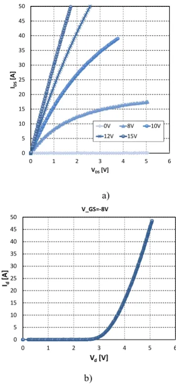
Fig. 1 shows the chips used in this study and Fig. 2 reports its output and body-diode forward characteristics [1]. As can be seen, the devices, with a nominal rating of 50 A, exhibit nearly a 4 to 5 times bigger cross-section than counterpart lower voltage rated SiC MOSFETs. Moreover, in view of the body-diode characteristics, they are clearly designed with synchronous rectification in mind for optimum performance.
Fig. 1. 3.3 kV-50 A SiC MOSFET chip. The die lateral dimensions are 7.2 x 7.2 mm2.
a) 0 5 10 15 20 25 30 35 40 45 50
0 1 2 3 4 5 6
Id
[A
]
Vd[V] V_GS=-8V
[image:1.595.343.522.247.640.2]b)
[image:1.595.99.230.499.672.2]Fig. 2. Measured MOSFET output characteristics, a), and body-diode forward characteristics, b), at ambient temperature.
Fig. 3 shows the measured temperature dependence of tehse characteristics: although, as expected, the increase of on-state
0 5 10 15 20 25 30 35 40 45 50
0 1 2 3 4 5 6
IDS
[A
]
VDS[V]
0V 8V 10V
resistance is more pronounced than the decrease of the diode forward voltage as the temperature increases, the advantages of adopting synchronous rectification for free-wheeling are manifest up to considerable operational temperature values.
a)
[image:2.595.66.247.113.429.2]b)
Fig. 3. Tempearture dependence of transistor output characteristics, a), and body-diode forward characteristics, b).
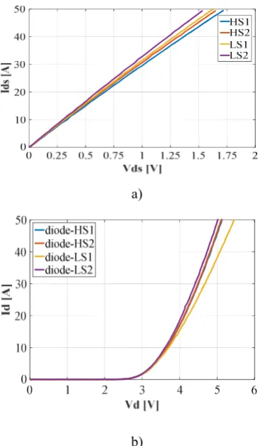
Finally. Fig. 4 shows the measured spread among 4 devices. The observed differences in the output characteristics could be relaled to a difference in threshold voltage of only some tens of mV, which is considered a very tight distribution in light of comparison with commercial products at lower voltage ratings. The spread in the body-diode on-state voltage is also very satisfactory in view of the high voltage technology maturity level. These results reasonably motivate the development of a multi-chip module.
II.MODULE DESIGN AND PROTOTYPE DEVELOPMENT The chips are assembled in a half-bridge switch architecture, as depicted in Fig. 5 a). Two parallel transistors are used for both the high-side and the low-side switch implementation to yield the target 100 A nominal current rating. As indicated in Fig. 5 a), in the case of high voltage transistors, both in reason of higher dV/dt capabilities and because of larger dies cross-sectional area for a given current rating, parasitic capacitance of the terminals switching at high frequencies, such as the middle point in the half-bridge architecture, become more relevant and require dedicated
attention in the development of a power module to avoid the circulation of excess common mode currents, which may severely impair the maximum achievable switching frequencies and transition speeds. This is true in particular of the more traditional assembly approaches, of the kind pursued here, which rely on the use of ceramic substrates soldered onto a baseplate, typically grounded.
a)
b)
Fig. 4. Measured spread in transistor output characteristics, a), and body-diode forward characteristics, b), for 4 devices.
So, the module design here is compatible with standard printed circuit board (PCB) mounting, but its design targets minimum and well balanced values of parasitic inductance and common mode capacitance towards the baseplate. The design formulated to jointly meet these design intentions is shown in Fig. 5 b): salient features of the module are:
- full separation of drive and power loops, to avoid interference of switching load currents with gate-loop parasitic inductance; the importance of the adoption of Kelvin-source type interconnects in the drive loop have been recently pointed out to be key in the case of SiC MOSFETs [2];
[image:2.595.336.518.142.456.2]only the chip cross-section is considered. However, the
minimum acceptable track size needs to be decided on the basis of the module thermal performance and, more precisely, needs to ensure uniform and symmetric electro-thermal performance among the chips. The dimensions shown in Fig. 3 are the final ones, deriving from thorough finite element based analysis of the thermal response of the module, with results as shown in Fig. 5 c);
- symmetrical parasitic inductance for the high-side and low-side switches;
- use of two separate smaller substrates for mounting of the transistors, so as to optimize ease of manufacturing and ensure good control of the quality of the solder underneath the substrate (that is, between substrate bottom-side copper track and baseplate).
Fig. 6 a) shows the assembled power module, fully covered in dielectric gel and ready for final encapsulation. The test setup is a single-phase inverter leg, designed so as to be easily modified into a double-pulse tester for initial experiments. One connoting feature of the test setup, visible in Fig. 4 b), is a heatsink equipped with both cooling fans and heating resistors, so as to decouple the switched power level from the baseplate temperature during the device and module characterization. a)
b)
c)
Fig. 5: a), schematic of a half-bridge switch with indication of common-mode capacitance, a major limiting factor for high dV/dt’s and switching frequencies; b), module layout, with fully symmetrical electro-magnetic paths, separation of drive and power loops and reduced drain-side mounting area for the low-side switch to reduce common mode capacitance; the devices are paralleled outside of the module; c), module thermal analysis showing uniform temperature distribution notwithstanding different track sizes.
a)
[image:3.595.57.267.95.598.2]b)
[image:3.595.332.535.338.642.2]III.EXPERIMENTAL TESTING
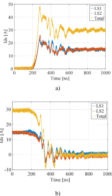
A parametric characterization of the switching performance of the module has been presented in [3]. In particular, is has been shown that the switching energy is virtually independent of the baseplate temperature over a broad range of temperature values. This finding confirms previous observations on lower voltage SiC MOSFETs, for which this particular feature has already been proven to be associated with disruptive possibilities to optimize system level power densities by joint optimization of the switching frequency and the heat-sink [4]. Here, results for the parallel operation of the transistors and their body-diodes are presented. Fig. 7 shows turn-on and turn-off switching current transient waveforms for the two transistors in the low-side switch; Fig. 8 shows the reverse recovery current in the body-diodes of the high-side-switch transistors, in a), and its stability over temperature, in b). The devices are being subjected to extensive testing pushing towards their actual limits in terms of both current and temperature. The results gathered so far indicate that the devices can be used well in parallel and achieve good power sharing even during fast transient events. Also, the body-diode works reliably and no signs of aging or any degradation have been detected.
IV.CONCLUSION
High voltage SiC MOSFETs are rapidly making their way towards becoming an industrial reality. While the technology maturity still needs further development to access a number of application domains, first results on the device performance considering both single and parallel chip operation are very encouraging, even with conventional packaging solutions.
ACKNOWLEDGMENT
The authors gratefully acknowledge the support of Mr. Takui Sakaguchi, Dr. Takashi Nakamura and Mr. Masaharu Nakanishi of ROHM Semiconductors, Japan, and Dr. Prasad Bhalerao of ROHM Semiconductors GmbH, Germany.
REFERENCES
[1] T. Sakaguchi, M. Aketa, T. Nakamura, M. Nakanishi, M. Rahimo, Characterization of 3.3kV and 6.5kV SiC MOSFETs, in Proc. PCIM2017, Nuremberg, Germany, 2017.
[2] C. Boedeker, E. Ayerbe, N. Kaminski, Impact of a Kelvin Source
Connection on Discrete High Power SiC-MOSFETs, in Proc.
ICSCRM2017, Washington D.C., USA, Sep. 2017.
[3] B. Mouawad, A. Hussein, A. Castellazzi, A 3.3 kV SiC MOSFET Half-Bridge Power Module, In Proc. CIPS2018, Stuttgart, Germany, Mar. 2018.
[4] E. Gurpinar, A. Castellazzi, Tradeoff Study of Heat Sink and Output Filter Volume in a GaN HEMT Based Single-Phase Inverter, IEEE Transactions on Power Electronics ( Volume: 33, Issue: 6, June 2018), 5226 - 5239 .
a)
[image:4.595.334.520.60.348.2]b)
Fig. 8: Transient switching body-diode turn-off current for two parallel transistors in the high-side switch, a); temperature stability of body-diode turn-off performance, b).
a)
b)
[image:4.595.63.249.349.674.2]