Implementing and communicating with SHILS
Master’s Thesis by
Remco Blumink
Committee: ir. P.T. Wolkotte dr. ir. A.B.J. Kokkeler ir. P.K.F. Hölzenspies
Abstract
Simulation can be used to check whether a design complies to its specifications. Digital hardware designs must be simulated cycle-true, bit accurate to verify timing. Performing such simulations takes prohibitively long for large hardware designs, i.e. a 6x6 NoC design requires 29 hours for simulation.
Simulation on an FPGA platform can be used to shorten the simulation time. However, a large hardware design can not be simulated in a single FPGA as a whole. To be able to simulate a large system using a single FPGA, the system is divided in sections (entities) that are simulated sequentially. The entities in homogeneous sys-tems are identical, the required logic for an entity can be reused for all entities when the state of the entities can be extracted. For extraction, a tool is provided. The re-sulting simulator performs simulations on a Design Under Test (DUT) sequentially.
To simulate a system in an FPGA, it must be supplied with stimuli and control. This thesis integrates the simulator in an FPGA design, referred to as SHILS. SHILS provides stimuli and control buffers, and a MMIO interface. SHILS is controlled by software in an embedded processor, it is a co-simulation system.
In order to extend the capabilities of SHILS, a design is proposed to link MAT-LAB to SHILS. The design is based on Xilinx System Generator, which arranges the communication between the MATLAB model and SHILS over Ethernet.
Contents
Contents iii
List of Acronyms vii
1 Introduction 1
1.1 Motivation . . . 1
1.1.1 Hardware-based simulation: emulation . . . 2
1.1.2 Sequential Simulation . . . 3
1.2 Assignment . . . 5
1.3 Thesis Outline . . . 6
2 Background 7 2.1 System design process . . . 7
2.1.1 Digital System Design . . . 8
2.1.2 Tool chain . . . 8
2.2 Co-simulation . . . 9
2.3 Sequential Simulator . . . 9
2.3.1 Simulator design . . . 10
2.3.2 Using SHILS . . . 11
2.4 Related work . . . 14
2.4.1 Hardware emulation systems . . . 14
2.4.2 Sequential Simulation . . . 14
2.4.3 Co-simulation . . . 15
3 Basic SHILS design 17 3.1 System structure . . . 17
3.2 Design . . . 18
3.2.1 Stimuli . . . 18
3.2.2 Stimuli Buffer design . . . 20
3.2.3 Output buffer design . . . 22
3.2.4 Interface bridge design . . . 23
4 Implementation 25 4.1 Platform . . . 25
4.2 Hardware implementation . . . 26
4.2.1 System Controller . . . 27
4.2.2 Memory-Mapped I/O interface . . . 28
4.2.3 Simulator . . . 29
4.2.4 Stimuli buffer . . . 29
4.2.5 Timecode checker . . . 30
4.2.6 Output buffer . . . 31
4.3 Software implementation . . . 31
4.3.1 Configure connection . . . 32
4.3.2 Test connection . . . 33
4.3.3 Configure simulation . . . 33
4.3.4 Run simulation . . . 33
5 Tool evaluation 35 5.1 Requirements . . . 36
5.2 Criteria . . . 36
5.3 Selected tools . . . 38
5.4 MATLAB . . . 38
5.4.1 MATLAB EDA link MQ . . . 39
5.5 Xilinx System Generator . . . 40
5.6 Altera DSP Builder . . . 40
5.7 CosiMate . . . 40
5.8 Ptolemy . . . 42
5.9 Simics . . . 42
5.10 Manual solution . . . 43
5.11 Comparison . . . 43
5.12 Conclusion . . . 46
6 Co-simulation system design 47 6.1 Requirements . . . 48
6.2 Global system structure . . . 48
6.3 Data transfer method . . . 49
6.3.1 Reuse MMIO interface in FPGA . . . 49
6.3.2 Add address generation to Field Programmable Gate Array (FPGA) . . . 49
6.3.3 Interconnection medium . . . 50
6.4 Xilinx-based design . . . 52
6.4.1 Performance . . . 53
6.4.2 Deployment effort . . . 53
6.4.3 Resources . . . 53
6.5 Conclusion . . . 53
7 Results 55 7.1 Simulator Scalability . . . 56
7.2 Scalability of stimuli buffer . . . 56
7.2.1 Storage scaling . . . 57
7.2.2 Control scaling . . . 57
7.3 Control buffer scalability . . . 57
8 Conclusion 59 8.1 Recommendations and Future work . . . 60
8.1.1 Improve conversion to simulator . . . 60
8.1.2 Better simulation control in FPGA . . . 60
8.1.3 Data compression of stimuli and output data . . . 60
CONTENTS v
A Memory Map 61
B Test case: IIR filter 65
B.1 IIR filter . . . 65
B.2 Homogeneous structure . . . 67
B.3 Challenges . . . 68
B.4 Results . . . 70
C C code listings 71
List of Acronyms
AHB Advanced High-Speed Bus
ASIC Application Specific Integrated Circuit
BCVP Basic Concept Verification Platform
CAES Computer Architecture for Embedded Systems
DSP Digital Signal Processing
DMA Direct Memory Access
DUT Design Under Test
EBI External Bus Interface
EDA Electronic Design Automation
EDIF Electronic Data Interchange Format
FIFO First In-First Out
FSB Front Side Bus
FPGA Field Programmable Gate Array
GPP General Purpose Processor
GUI Graphical User Interface
HDL Hardware Description Language
HIL Hardware-in-the-loop
IC Integrated Circuit
IIR Infinite Impulse Response
ISE Integrated Synthesis Environment
LUT Look Up Table
MMIO Memory Mapped In-/Output
NoC Network on Chip
OSI Open Systems Interconnection reference model
SoC System on Chip
SHILS Sequential Hardware-In-the-Loop Simulator
RAMP Research Accelerator for Multiple Processors
RTL Register Transfer Level
CHAPTER
1
Introduction
1.1 Motivation
When a system is designed, it is important to know whether the design iscorrect. Knowledge on this matter is evenly important for digital systems and digital hardware designs. Technology for digital systems has evolved greatly because of advances in Integrated Circuit (IC) technology. More flexible chips have become available, like Field Programmable Gate Arrays (FPGAs) and nowadays a complete system is constructed on a single chip (a System on Chip (SoC)) instead of several chips mounted on a Printed Circuit Board(PCB). Also, there is a tendency to design multicore processors, possibly connected to each other via a Network on Chip (NoC). Development of a SoC is a very complex task, but can be structured by the sep-aration of communication and computation. This can be implemented by means of a NoC [2]. Still, errors and mistakes are introduced in system design. SoCs can be realized in an Application Specific Integrated Circuit (ASIC). Production of an ASIC is extremely costly. Therefore, design errors need to be eliminated. Besides design verification, the facility to optimise the network’s parameters is desirable to achieve the best possible results.
Before continuing, several terms should be defined to avoid confusion.
Definition1(Verification): Based on acompletespecification (using pre- and post-conditions), give a solid proof that the postcondition holds given the truth of the precondition. Thus, if the precondition does not hold, the postcondition needs to fail too. This also holds for the system’s specification and its implementation.
In verification, an important assumption is that a system is accurately specified by means of pre- and postconditions. That is to say, if the precondition is true before an execution of the system starts, then the postcondition must be true after execu-tion. If a system is specified using pre- and postconditions, than its correctness can beformally verified(proved): just assume that the precondition holds for all input of the system, and prove that the output satisfies the postcondition. However, in practice this technique is only possible for fairly small components of a system, the system as a whole is often too complex to be proven correctly in a formal way. In real life, the best way to check whether a system is correct, is by simulation:
Definition 2(Simulation): To represent the behaviour of a design by using another system, for example by a computer program designed for this purpose. Characteristic is that simulation should imitate the internal processes and not necessarily deliver the results of the design that is simulated for the purpose of detailed analysis and prediction. Also, the execution time of the simulated entity does not necessarily match the real time.
The term verification by simulation is used when applying simulation to check the correctness of a system. This is not formal verification as only can be proven that in certain conditions a system will fail or pass. Nevertheless, verification by simulation is often used in system design to replace formal verification.
Using simulation, the behaviour of a design can thus be examined. Simulation of a synchronous digital system is possible at multiple abstraction levels, but is mainly performed at two levels: abstract (behavioural) and cycle-accurate (precise). Be-havioural simulation focuses on the way a design behaves, the exact number of clock cycles an operation requires are not taken into account. An advantage of this method is that behavioural simulation is reasonably fast to compute on a normal PC. Simu-lation is completed in an acceptable amount of time.
Another, often used, method is cycle-accurate or cycle-true simulation. The main difference with behavioural simulation is that timing is included in simula-tion. Each operation takes exactly as many clock cycles as a real ASIC. Calculating all states in each time step creates a greater computational complexity, which even-tually leads to prohibitively long simulation times when designs are large. For exam-ple, a 6x6 NoC described in the SystemC language requires 29 hours to complete [39]. When simulating a complete system, only system-wide details are required by the user. Internal details are required for precise timing and are thus calculated every simulation step although system-wide data is examined.
1.1.1 Hardware-based simulation: emulation
Due to the problems which arose with the time needed to complete a cycle-accurate simulation, and the availability of parallel hardware, several initiatives started to in-vestigate the possibilities of using FPGAs for simulation. By creating the hardware in the FPGA, the simulated design can be operated fully in parallel instead of sequen-tially in software on an ordinary PC. This will reduce the total simulation time by several factors.
Performing simulation in physical hardware is sometimes also referred as emu-lation. For the sake of completeness, emulation is defined in definition 3.
Definition3(Emulation): A system which is behaving exactly as a real system, but is mapped to a different system. The main difference with simulation is that to the system’s environment, the system acts fully identically compared to the system it replaces. It is possi-ble to replace a real design with an emulator in a system without notice of the other system parts. For developers/debugging, an emulator often provides for several facilities to monitor variables inside the emulator.
Several research initiatives started exploring the use of emulation for verifica-tion of designs, which are discussed in more detail in secverifica-tion 2.4.
1.1. MOTIVATION 3
. .
Streaming data is a model which is used when large quantities of data arrive continuously. Characteristic is that storage of this data is not needed for a long period, as it is either impractical, or just unnecessary. There are several applications which naturally generate vast amounts of data which arrive continuously, instead of simple sets of data arriving accidental, for example multimedia applications (IPTV etc.), financial markets and news organizations [28].
Focus of the University is mainly at multimedia applications.
.
Intermezzo:Streaming data
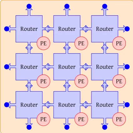
These streaming applications are mapped on homo- and heterogeneous tiled architectures which often incorporate parallelism and have a more or less regular structure, composed out of a lot of identical components. An example of this is a SoC build of 9 elements interconnected via a NoC as shown in figure 1.1. The processing elements (PE) in this figure are displayed smaller than the router for ease of drawing. This is not necessarily the case in reality.
[image:13.595.161.374.338.550.2]. . . Router . PE . Router . PE . Router . PE . Router . PE . Router . PE . Router . PE . Router . PE . Router . PE . Router . PE
Figure 1.1: System on Chip Example
Systems that are just slightly larger than this example (like a NoC of 6x6 ele-ments), are virtually impossible to simulate in software [38]. Therefore, research effort has been put into the development of a dedicated simulation system.
1.1.2 Sequential Simulation
time-multiplexing [12, 39]. System-level simulations are then performed sequen-tially in parallel hardware instead of parallel on a sequential system.
A digital system is represented by its state and logic. When logic and state be-come too large, it is not possible to update the entire state at a single moment due to resource constraints in an FPGA.
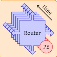
It is possible to partially update the state of a system. This is achieved by divid-ing the state is into several sections, which are then sequentially updated. These sections are referred to as entities. The number of logic needed to update an indi-vidual section of the system state is significantly less than the required logic for the entire system. Common functionality of entities can be shared by all state updates of individual sections. The logic can be reused, therefore fewer resources are required. This enables the use of a single FPGA for simulation of the entire system (when the entity requires no more resources than available in a single FPGA). The example sys-tem shown in figure 1.1 can be simulated in sections based upon the reuse of logic from single router and processing element. The modification of the figure is shown in figure 1.2.
. . .Router
[image:14.595.272.367.327.422.2]. PE . Router . PE . Router . PE . Router . PE . Router . PE . .time
Figure 1.2: Sequential System on Chip Example
The state of digital synchronous systems can alter both on the rising edge and the falling edge of the system clock. Therefore, the entire system should be evaluated for both parts of a clock period. An entity can be simulated during each simulation cycle. A single instance simulation cycle is addressed as delta cycle for readability. An example system consisting of four identical parts requires eight simulator clock cycles to complete simulation of one system clock cycle, which is shown in the ex-ample schedule in figure 1.3.
.
.Simulation clock .
.t=0 .t=1 .t=2 .t=3 .t=4 .t=5 .t=6 .t=7 .t=8 .System clock
.
Simulated entity
.
One full system simulation cycle
.
Single instance evaluation .
#1 .#2 .#3 .#4 .#1 .#2 .#3 .#4
Figure 1.3: Global simulator time line
[image:14.595.166.473.558.660.2]1.2. ASSIGNMENT 5
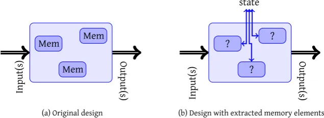
registers and other memory elements are replaced by custom components that link to an external storage location for their values. Thus instead of an entity with some memory elements shown in figure 1.4a, the memory elements are replaced with a component that fetches and updates the corresponding element of external state as shown in figure 1.4b. By storing the entire state of a system in an external memory, more efficient storage is provided compared to flip-flops as the density of RAM in FPGAs is much higher compared to that of registers.
In this way, at any moment in time, only a small section (a single entity) of the entire system is used in the simulator. Therefore, the number of required resources are much lower than for the complete system. In homogeneous systems the logic for most entities is identical, which lowers the required resources further.
. . . Mem . Mem . Mem . .Input(s) . .Output(s)
(a) Original design
. . . ? . ? . ? . .Input(s) . .Output(s) .state
[image:15.595.113.431.283.399.2](b) Design with extracted memory elements
Figure 1.4: State extraction example
Of course, emulating a system sequentially requires more time than a fully par-allel system, but this is several orders of magnitude faster compared to simulation in software. To control the simulator, hardware is added to the FPGA.
Efforts from Rutgers [33] at the University of Twente delivered a tool which:
1. Automatically extracts memory elements out of a design.
2. Provides a wrapper around the transformed entity, which provides memory for the extracted state of the simulated entity and the links between entities. Rutgers has also provided in the simulator, to which is referred as “the simulator” in this thesis.
The simulator requires external control and the simulator should be provided with stimuli. The simulator is designed to operate in a system consisting of an FPGA that houses the simulator and a processor to provide it with stimuli, according to the Hardware-in-the-loop (HIL) principle. However, the external interface of the sim-ulator is not directly linked to any physical interface like a Direct Memory Access (DMA) interface. The simulator is also not equipped with buffering capabilities for both stimuli and the output data of simulated entities. Therefore, the simulator de-livered by Rutgers is not yet able to perform simulations.
1.2 Assignment
section discusses the problems dealt with in this thesis. The main focus of this thesis is:
What measures are needed to connect a stimuli generator and an anal-ysis program operating on a PC to the sequential simulator operating in an FPGA?
This question is based upon two pillars, which explain why this problem is discussed in this thesis.
First, the simulator delivered by Rutgers was not ready for usage in the FPGA. A major concern is that the simulator and processor operate at different clock frequen-cies. Also, the frequency of producing and consuming differs. Therefore, buffering is required. The first part of this thesis is thus focused at:
How to implement the simulator in an actual FPGA, how to connect it to a processor and how to make them communicate?
Second, as noted in [38, 39], there is a significant effort required of a small pro-cessor for stimuli generation. Since a PC is equipped with a much greater amount of processing power, it is very interesting to replace this processor with a PC to save more processing power for analysis and control tasks. Also, software is available for data generation and analysis. The second question is formulated as follows:
How to connect a PC with the sequential simulator on the FPGA, how to make them communicate and process data?
The PC-based simulation system must have better performance than the system us-ing an embedded processor. Also, tool chain integration is important for more easy generation of stimuli and analysis.
For readability, SHILS is used to refer to the complete sequential simulation sys-tem hardware. Stasys-tements on the simulator exclusively apply to the simulator de-livered by Rutgers.
1.3 Thesis Outline
CHAPTER
2
Background
This chapter introduces a number of topics, which are important for the SHILS dis-cussion, they create the context for it.
Before describing the sequential simulator in detail, its role in the system design process should be pointed out. Therefore, the normal system design process is dis-cussed first. The sequential simulator is designed to aid in the verification process of a design. Using the sequential simulator in an existing design does not require many additional steps, but requires attention throughout the entire process.
SHILS is a co-simulation system. Co-simulation is discussed in general in sec-tion 2.2.
The discussion of sequential simulation also introduces the sequential simulator design of Rutgers [33] in more detail, focused towards usage of the simulator.
2.1 System design process
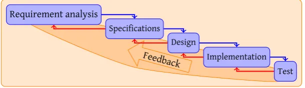
The design process is based upon the Waterfall model, which is briefly discussed next.
The Waterfall model (shown in figure 2.1) is a very well known model, introduced in 1970 by Royce [32]. In this iterative model, each successive step adds more detail to a design. The main benefit of this approach is that the number of changes is man-ageable, and it is possible to return to an earlier phase if unforeseen problems occur. This process is referred to as feedback.
.
.
.Feedback .
Requirement analysis .
Specifications . Design
.
[image:17.595.113.418.606.694.2]Implementation . Test
Figure 2.1: Waterfall model
2.1.1 Digital System Design
The methodology of both ASIC and FPGA design are identical, the main difference is the tooling which is used. Therefore, a design that shall be produced in an ASIC, is testable in an FPGA.
A design can be specified at several levels, but most digital systems are designed using a Hardware Description Language (HDL), specified at Register Transfer Level (RTL). The sequential simulator also is designed at RTL. This discussion of digital system design is therefore focused at RTL level.
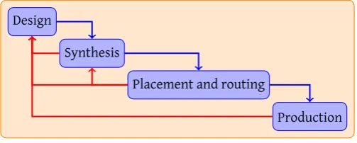
Globally, the design process can be divided into three steps, as shown in fig-ure 2.2. The Waterfall model is applicable to these steps, and to the internals of the design phase. Verification of a design, the goal of SHILS, takes place prior to the production.
.
. . Design
.
Synthesis
.
Placement and routing
.
[image:18.595.194.446.288.389.2]Production
Figure 2.2: Global design process
The synthesis phase translates the RTL design into technology dependent cells that perform a certain function, like flip flops and multiplexers and deals with in-terconnection of those cells. This is performed in two tasks:
1. Assemble all system parts to create a single integrated system
2. Translate the logic cells in the design to technology dependant cells
Subsequently, the placement and routing phase then performs two tasks:
1. Map the assembly of logic cells to a grid of available resources. In FPGAs the Look Up Tables (LUTs) are mapped into a suitable physical position on the chip.
2. Connect the logic cells which are used in the grid of an FPGA.
In the end, the production phase generates a programming file for an FPGA. The designer is mostly involved in the first phase. Tooling can solve the other phases. In special cases, the designer influences the solutions of the tooling. Still, designing remains an iterative process with feedback from previous phases, even automated tasks generate feedback that should be used in preceding phases.
2.1.2 Tool chain
2.2. CO-SIMULATION 9
speed for behavioural descriptions. Bit-accurate, cycle-accurate simulations con-sume quite a lot of time.
PrecisionSynthesis is used for synthesis. This tool, also from Mentor, is used to translate a RTL description to industry standard Electronic Data Interchange Format (EDIF). This describes the logic cells which will be used to physically realise the RTL description.
Finally, the placement and routing phase is performed by Xilinx Integrated Syn-thesis Environment (ISE). This tool accesses several tools internally:
1. ngdbuild, which combines all subparts into a single file combined with con-straints.
2. map, which maps the logic cells to the actual cells.
3. par, which places the cells at positions on the FPGA and interconnects them
4. bitgen, which generates the programming file
The tool flow can be highly automated. This saves the designer time and in-creases the ease of use, and a single command can be used to perform both synthesis, and placement and routing.
2.2 Co-simulation
Verification of a design using SHILS is closely related to co-simulation. Therefore, co-simulation basics are briefly introduced.
Embedded systems are often multidisciplinary, spanning between between pure software design, pure hardware design and mechanics. These disciplines require a combined methodology to create a system. Co-simulation is a powerful technique in virtual prototyping to provide a solution for this [16].
Co-simulation is a simulation which spans across multiple disciplines, and can be performed within a single simulation package capable of performing multidisci-plinary simulations, or by connecting several simulators specific for each discipline. For example 20-sim [6] and Ptolemy [4] can be used for multidisciplinary simulations. A number of simulators specific to a discipline can be linked with a separate in-frastructure that deals with interconnection of these simulators [10] or by linking the simulators directly together [26].
Several co-simulation environments already incorporate a form of distributed simulation. By distributing the simulation across multiple PCs, it is possible to in-crease the overall simulation speed as the available processing power is inin-creased. A similar approach could be used to connect the sequential simulator in the co-simulation environment although most co-co-simulation approaches use only software for simulation.
2.3 Sequential simulator introduction
The process of extracting memory elements from a design is extensively cussed by Rutgers [33, chapters 2 and 3]. Usage of the transformation tool is dis-cussed in section 2.3.2.
2.3.1 Simulator design
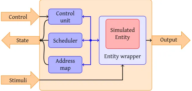
The simulator framework designed by Rutgers is globally divided into four main blocks. These are depicted in figure 2.3.
. .
. .
.
Simulated Entity
.Entity wrapper .
Scheduler
.
Address map .
Control unit
. State .
Control
.
Stimuli
.
[image:20.595.158.481.233.387.2]Output
Figure 2.3: Global simulator design
As shown, the simulator is wrapped around a simulated entity. The entity is not an integral part of the simulator, it is purely for simulation of a specific Design Under Test (DUT). To match the entity to the standard interfaces used by the simulator, a separate wrapper is provided by the transformation tool. This wrapper also holds the storage for the DUT’s state and deals with linking the entities of the DUT together in simulation; the wrapper is discussed in more detail by Rutgers [33]. The wrapper is controlled by the control unit and signals when the system can advance to a next delta cycle when the DUT has stabilised after data of a next entity has been offered. Input ports of DUT entities that are not connected internally must be supplied with data. The stimuli input of the simulator provides this data. The simulator is not equipped with any logic to check input data correctness at any moment, it requires data to be ready at the moment it needs the stimuli. The output of entity instances can be examined via the output port. The simulator control state is accessible via an output port.
The simulator is controlled using a set of commands, i.e. “RUN CYCLE”, defined by Rutgers. Another command is used to initialize connections between entities in a DUT. For each connection, the arguments of this command specify:
• Which input port reads from what entity instance?
• Which input ports are connected to the stimuli input(if any)?
• Which output port writes to what entity instance?
2.3. SEQUENTIAL SIMULATOR 11
with a vector of entities that are dependant of the entity instance that is currently simulated by the address map.
The scheduler determines which entity instance is simulated next. The imple-mentation of Rutgers uses a fairly basic Round Robin scheduling mechanism.
The dependency vector is important for the scheduler as an entity instance might change the input of a previously simulated entity instance, that must be re-scheduled for simulation. Information on changed outputs is gained from the entity wrapper. Re-scheduling is depicted in figure 2.4.
.
.Simulation clock .
.t=0 .t=1 .t=2 .t=3 .t=4 .t=5 .t=6 .t=7 .t=8
.System clock
.Simulated entity .#1 .#2 .#3 #1. .#1 .#2 .#3 .#2
Figure 2.4: Re-scheduling example
To improve performance, the simulator is pipelined. Several steps must be taken before an entity instance can be simulated, which can be performed simultaneously for several instances. Pipelining boosts performance of the simulator, it is capable of processing an entity instance each clock cycle. These simulation cycles are referred to as delta cycles. To complete a system cycle, the simulator must process simulation of all entities for both the “high” period as well as the “low” period of the system clock. This is also depicted in figure 2.4
2.3.2 Using SHILS
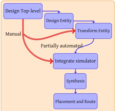
To start using SHILS, several steps should be followed. The entire system is too large to simulate in an FPGA. Therefore, the top level description is not usable for simu-lation, but it is the starting point in the design flow. The system design flow divides into two separate flows, which is depicted in figure 2.5 and discussed next.
The flow of information indicated in figure 2.5 with “manual” must be performed manually for now, as information that is described in the top-level description can-not be extracted automatically yet [33]. The developer should extract the following information manually:
1. How many entities are simulated?
2. How are entities interconnected?
3. What are the global clock and reset signals?
These questions are used in the translation process, and in the actual simulation runs.
.
. .
Design Top-level .
Design Entity
.
Transform Entity
.
Integrate simulator
. Synthesis
.
Placement and Route .Manual
[image:22.595.207.430.124.339.2].Partially automated
Figure 2.5: Sequential simulator design process
Transform entity
Memory elements in an entity are automatically extracted by a transformation tool delivered by Rutgers [33]. Besides the entity, the tool requires a number of basic arguments:
• The set of possible links between the ports of an entity
• How to order ports internally
• Specification of which signal to use for clock and reset
To specify these arguments, the information gathered in the manual sub flow(section 2.3.2) is used. Rutgers defined additional arguments for several purposes [33, chapter 4].
This tool operates on EDIF files only. Therefore, the design specified in Very High Speed Integrated Circuit Hardware Description Language (VHDL) should be synthe-sized prior to transformation. The transformation tool requires a number of options to be set in synthesis:
• Do not generate I/O pads
• Preserve hierarchy
This is required for correct integration in SHILS after transformation. Precision-Synthesis, which is used at the CAES chair, uses the following commands to set the required options:
setup_design -addio=false
set_attribute -design rtl -name HIERARCHY -value preserve NAMEOFENTITY update_constraint_file
2.3. SEQUENTIAL SIMULATOR 13
The transformation tool is run using a Makefile, which automatically executes several steps to deliver several items:
• Transformed entity in EDIF and Xilinx-proprietary NGO format1 as well as
VHDL format that can be used for simulation.
• Entity wrapper in VHDL format
• VHDL package with correct bit widths, port specifications etc.
Integrate entity in simulator
After transformation, the entity is integrated in the simulator. Some data widths are not adjusted automatically and should be modified. The simulator integrated in the rest of hardware design, described in chapter 3.
SHILS is then integrated and synthesised using the tool flow described in sec-tion 2.1.2. The synthesis tool integrates the transformed entity into the simulator during synthesis of SHILS.
Simulator usage
The synthesis tool generates a programming file which can be inserted in the FPGA. Before simulation, several configuration variables must be set. The transformation tool does not extract these variables automatically, the information gathered in the manual sub flow (section 2.3.2) is therefore used. Configuration is done at run-time, and can be changed if desired (reset is required). These configuration variables are:
Number of simulated entities The simulator is capable of simulating a certain maxi-mum number of entities. This number is set manually in the simulator VHDL code. Per simulation it is selectable how many entities are used for simulation.
Initialize connections between instances Inside the simulator, link memories are used to store data for input of other entities. Per entity, three configuration variables must be set. These are:
• Which input port reads from which entity
• Which output port writes to which entity
• Which input port is connected to external stimuli (if any)
The simulator internally uses different memories to store the read and write actions on entity ports. Therefore, these must be specified separately.
With these configuration steps, the simulation can be run. Of course, for input ports of simulated entities that should be supplied with stimuli, data should be ready.
2.4 Related work
As introduced in chapter 1, research for simulation of large embedded multipro-cessing designs has been extended with (at least partial) hardware-based simulation. Several approaches exist, which are discussed in this section.
The software industry tends towards multiprocessor systems because of the “brick wall” [21]. Compared to research in NoC and SoC verification, there are similarities with ordinary software research in multiprocessing. FPGAs have attracted the atten-tion of software researchers, too due to their flexibility and scalability. According to Chung et al. [12] a slowdown of about 100x in an FPGA compared to a real multi-processor is acceptable for software research. This figure is supported by figures of Olukotun et al. [29]. Ideas used in this research field are also applicable in simulation and verification of SoC and NoC designs.
2.4.1 Hardware emulation systems
There are several initiatives to port a basic multiprocessor system to an FPGA-based platform and to realise a basic infrastructure for simulating a large number of pro-cessors. For example the Research Accelerator for Multiple Processors (RAMP) project [3], can simulate up to 1024 MicroBlaze processors. This project is heavily sponsored by Xilinx and Intel, and has already delivered a few versions of a prototyping board, like BEE2 [9]. This approach is costly, as a single board costs about 20.000 USD and a complete simulation system is constructed out of several of these boards.
2.4.2 Sequential Simulation
Another — cheaper — approach is started by Chung et al. [11, 12] in the ProtoFlex project. The ProtoFlex project is carried out in conjunction with the RAMP project. They present a system which uses time-multiplexing to save FPGA resources and a clever hybrid mechanism to keep implementation complexity low, running at the BEE2 board [9]. The time-multiplexing mechanism used by ProtoFlex is very similar to that of SHILS, an interleaved pipeline is used to sequentially simulate all CPUs which are simulated. The idea behind the ProtoFlex approach is that computation-intensive and often used tasks are performed directly on the FPGA, whereas less used tasks are performed in software. The tasks that are executed by software are either executed in a soft-core processor residing in an FPGA or in an external PC, connected via Ethernet [12] to the FPGA board. A speedup of 39x compared to common used multiprocessor simulation software is obtained [12].
Parashar and Chandrachoodan also present a sequential simulation framework [31]. They present an algorithm intended to simulate synchronous systems of log-ical processes, using events and a simulator to test their algorithm. The algorithm is for simulation using very basic processing elements, and it eliminates the need to sort the events of single queue event based simulation algorithms. Those pro-cessing elements only support simulation of the straightforward Boolean functions AND, NAND, OR, NOR, XOR, XNOR, and NOT, and simulation of an edge-triggered D-flipflop. Nothing is stated about more complex operations. The cycle-true simulator is transaction-based in which scheduling of processing elements occurs at compile time.
2.4. RELATED WORK 15
fits in a medium sized FPGA(Xilinx Spartan XC3S1200E) after synthesis. The pro-posed algorithm is only tested in the ModelSim simulation software, not in physical hardware.
2.4.3 Co-simulation
Several systems create a co-simulation system, a simulation system assembled of both hardware and software. A considerable number of resources is required to im-plement a complete simulator in hardware. Therefore, several initiatives propose to use the versatility and power of an ordinary General Purpose Processor (GPP) for stimuli generation and analysis combined with the parallel simulation capabilities of FPGAs for the actual simulator.
The aforementioned ProtoFlex project [11,12] applies this form of co-simulation, primarily to save time and resources from implementing rarely used functionality in hardware. The key concepts behind this approach have been discussed in sec-tion 2.4.2.
Another example of co-simulation is proposed by Ou and Prasanna [30]. They use co-simulation in an entirely different manner; the novel aspect in their approach is the usage of high-level cycle-accurate abstractions of a low-level implementation to speed up the simulation process. MATLAB is used for the high-level abstractions. The origin of their approach is in the increased usage of soft core processors on FPGAs, and those processors are more customisable than normal processors. Certain parts can easily be performed in hardware, whereas other parts are executed within the soft core. By replacing the FPGA hardware with MATLAB connected to the soft core, complicated calculations can be performed at high speeds with hardware en-suring cycle-accuracy. Simulation of programs executing in a soft core processor is difficult within low-level simulation software like QuestaSim, therefore execution on a target platform is required to benefit fully from the speed-up.
Genko et al. [19] present another approach primarily intended for NoC feature exploration. Their approach uses a Xilinx Virtex 2 Pro (v20) FPGA as hardware plat-form to emulate NoCs. The system offers designers a platplat-form to quickly character-ize performance figures of a NoC, without loosing cycle-accuracy. A speed up of four orders of magnitude compared to cycle-accurate HDL simulation is reached accord-ing to the presented results. Different from other approaches is that this platform is suited purely for NoC emulation. Within the FPGA, several NoC topologies can be simulated without re-synthesis by software configuration. Primary results are latency statistics.
The presented results are based on relative small networks; presented figures are for a 2x2 mesh network. Scalability of this approach within a single FPGA is therefore poor.
Other examples of co-simulation are introduced in [16] and [35].
anal-ysis. Their approach reduces the amount of communication by a factor of 15 to 67, which results in an overall speed-up factor of 4-40 compared to existing lock-step simulation.
Co-simulation systems distribute functionality. One can argue that challenges are similar to those of distributed computing systems; therefore the problems and solutions discussed by Tanenbaum and Van Steen [34] for distributed systems, such as data consistency and data distribution, are also applicable to the co-simulation field.
CHAPTER
3
Basic SHILS design
Earlier, it was not yet possible to test the simulator of Rutgers [33] in real hardware, due to the lack of a physical interface with a controller (i.e. a GPP).
To connect the simulator shown in figure 2.3 with the physical world, a unified interface should be used to offer a sturdy connection with simulator control and analysis software.
3.1 System structure
The system is supplied with control and data by an external processor that is con-nected to the simulator. In this way, the system shown in figure 3.1 is created.
. .
. .
.
Stimuli Generator
.
Analysis of data
.
System control
.
Simulator
.
Stimuli buffer
.
Output buffer
.
System control .Processor
.FPGA
Figure 3.1: Global System structure
The figure shows the division of tasks between the processor and FPGA, as pro-posed by Wolkotte [39]. This balances both performance as well as flexibility. The interfaces require buffering of the input stimuli, output data and control. These are designed in the FPGA.
Hardware design is related to the targeted technology. The simulator design of Rutgers is not technology dependant, but the transformation tool is currently tailored to Xilinx technology dependant EDIF files.
3.2 Design
The SHILS FPGA design consists of several blocks. This design also incorporates an interface bridge for a GPP’s interface. Processors connected to an FPGA often operate at different clock frequencies than the blocks in the FPGA. As a result of this, clock domain transformations are required. This needs to be added to the implementation of the glue logic for certain parts of the system, which is called clock stretching. The blocks in which SHILS is divided are shown in figure 3.2, that also shows the primary flow of data, control and state in the FPGA.
The hardware design of Rutgers [33] is extended with:
• Stimuli buffer
• Output data buffer
• Control buffer
• Interface bridge
The design of these aspects is discussed in the following sections.
.
.
.
Simulator
.
Stimuli buffer
.
Output buffer
.
Control buffer
.
Interface bridge
. to GPP
.Data
.Control .State
Figure 3.2: System design block diagram
3.2.1 Stimuli
This section discusses general aspects of stimuli which are of importance for the design of the stimuli buffer.
3.2. DESIGN 19
The least efficient method of offering stimuli to a system is by sending new data preciselyat the moment it is required to change. It is very impractical; as the tight coupling requires that the producer and consumer of stimuli operate fully synchronous or use a tight handshake mechanism. A more flexible link is required that decouples production and consumption rates and times.
Stimuli are generated in a GPP as shown in figure 3.1. The operating frequen-cies of the GPP and FPGA differ; clock domain transition signals that are fully syn-chronous are hardly possible therefore. Because the amount of communication that is required to keep the system synchronized is very high.
To reduce the communication overhead, several measures are possible:
• Compress stimuli in time
• Produce stimuli in the FPGA
• Compress stimuli in space
Compress stimuli in time
Stimuli will not change every clock cycle, therefore not every clock cycle a sample should be transmitted. To be able to offer data efficiently in this case, a sample is ap-pended with a time stamp. This time code directs the earliest moment at which the stimuli buffer is required to offer the data to the simulator. Compression of stimuli in time is also used by Wolkotte [39].
Adding a time code to stimuli requires additional storage and communication. If stimuli is changing each clock cycle, this is not the best solution to reduce the quantity of date that is transmitted. To reduce the number of bits needed for the time code, relative timing could be used — the time code then signals the number of clock cyclesbetweentwo samples.
Produce stimuli in FPGA
To completely eliminate the clock domain transformation, the stimuli generator could also be moved to the FPGA. This can greatly enhance the system’s perfor-mance, but significantly limits the flexibility for the designer. This lowers the gen-erator speed, as most FPGAs operate at much lower clock frequencies than GPPs. A less restrictive solution is to generate a time code in the FPGA for stimuli that is generated in software. Time compression is applied in this manner without the ad-ditional communication overhead.
Compress stimuli in space
Data compression is a method which is often used to reduce the number of bits re-quired to transmit data. Previously, no data compression methods have been ap-plied to SHILS. As limited experience with data compression is available, this is left as future work.
SHILS approach
As the addition of a timestamp has already been successfully used by Wolkotte [39], it has been chosen to design the system using this approach. Time compression also offers a lot of flexibility and configurability for the stimuli generation mechanism.
3.2.2 Stimuli Buffer design
Figure 3.1 shows that stimuli are generated in a GPP. The link between GPP and SHILS requires the translation of the clock domain. The frequency at which stimuli is generated and consumed differs. The producer and consumer of stimuli must be decoupled for this reason too. Buffering is required to convert clock domains and to decouple producing and consuming frequencies. By decoupling the operating fre-quency of the simulator and stimuli generator, several issues are introduced, focused towards efficient transport of the data through the buffer.
The buffer has to maintain data consistency — the order in which data enters the buffer should be preserved. This avoids nondeterministic behaviour in simulation and analysis. In many cases generates the stimuli generator blocks of samples, which must be inserted in the buffer rapidly. For optimal data consistency, a useful feature is an interrupt mechanism. When the buffer is almost empty, the processor has to fill it fast. Another option is to temporary pause the simulator in the FPGA, but this has a significant performance penalty.
The simulator has no facilities to control the input stimuli. It just expects data to be available at the moment. Therefore, the buffer also has to be capable of extracting the oldest element out of the buffer and offer it at the right moment in time to the simulator.
Simulated entities can have multiple inputs, for example multiple ports of a router in a NoC. SHILS should be able to supply data for all these inputs. When mutual ex-clusion is ensured, a single buffer could be shared by multiple ports to reduce re-source usage. The simulator knows which port accepts a sample at what moment, therefore the same element can be offered to both ports simultaneously. Still, for input ports which are accessed by the same entity at the same moment, separate buffers or data outputs should be used. This also partially holds for multiple ports within the same clock cycle, an identifier could be used to signal which entity needs which data. The most straightforward method to create a buffer for all inputs is to provide a unique stimuli buffer for each input port. This allows data to be consumed by multiple input ports in parallel. Of course, this approach requires the most re-sources.
3.2. DESIGN 21
.
.
.
Processor clock .Simulator clock
. Select stimuli source . Stimuli generator . FIFO buffer . Timecode checker . Buffer
controller .Stimuli buffer
.Data in .Data out
.
[image:31.595.101.421.383.685.2]Control
Figure 3.3: Stimuli buffer block diagram
Stimuli buffer output timing
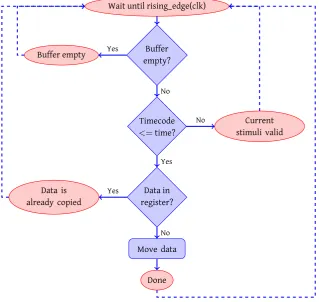
As noted, the simulator cannot control its stimuli input, it expects data to be avail-able. A separate component is introduced to offer stimuli at the designated moment to the simulator: thetime checker. This component compares the current time with the timestamp of the stimuli element that is the oldest in the FIFO buffer.
.
.
Wait until rising_edge(clk)
. Buffer empty? . Timecode <=time? . Data in register? . Move data . Done . Buffer empty . Current stimuli valid . Data is already copied . No . Yes . No . Yes . No . Yes
It monitors the top register of the FIFO buffer, and copies its value to the output of the stimuli buffer at the intended moment. The process of checking the timestamp is depicted graphically in figure 3.4. To decouple the stimuli buffer and simulator, the checker does not offer stimuli directly to the simulator, it only extracts the cor-rect sample from the buffer. The precise moment at which it is offered is arranged by the interface bridge. Data is ready within one delta cycle.
Timing is important in this stage. Based on [33, figure 5.2], timing of the sim-ulator regarding stimuli is shown in figure 3.5. To clarify the steps, a single flow through the pipeline is shown. In reality, each delta step a new address is generated and thus a sample should be available.
. .Simulation clock
.t=0 .t=1 .t=2 .t=3 .t=4 .t=5
.Step signal of simulator controller
.Generate next address .X .addr .
.Fetch input .XXX .val .XXX
.Input data and state registered .XXX .val .XXX
.Simulation
.Output of the entity .XXX . . .XXX
.
.Read address . . .XXX
.Stimuli ready
.
[image:32.595.165.473.257.471.2]Stimuli related
Figure 3.5: Timing diagram based on Rutgers [33]
After the controller of the simulator has given the “step” signal, the address of the instance that is simulated next is generated. It is available at the next rising edge of the clock. If the instance corresponding to the generated address requires stimuli, data is copied from the output register of the stimuli buffer to the stimuli input at t=1. This is determined by the developer. At t=2, is the stimulus ready for the simulator and copied to an internal register. At t=3, all data is ready for simulation, thus the actual simulation is performed at this moment in time. At t=4, the simulation of this delta cycle is done.
The simulator is pipelined. This indicates that stimulus must be buffered for 2 clock cycles in the pipeline.
3.2.3 Output buffer design
3.2. DESIGN 23
All data in the buffer should be accessible. Therefore, the entire buffer contents must be readable by the processor, which makes it similar to the producer side of the input buffer.
3.2.4 Interface bridge design
To connect all hardware parts with a GPP, an interconnection block is required. This provides glue logic to translate the data signals, which are used in the hardware, to a unified interface that connects to the GPP.. Also, clock domain translations are per-formed by the buffers of the interconnection logic. Clock domain transformations for the system’s control are performed by the control buffer. This buffer retains the same value for a minimal of one SHILS simulator clock cycle, which implies that this is the maximum frequency at which new commands can be issued by a GPP. In this way it is ensured that the command is received correctly.
The interface bridge connects the external interface to:
• Stimuli buffer
• Output buffer
• Simulator control via clock stretch buffer
• Simulator state
Also, the connector manages the overall system and provides internal connec-tions between certain parts. Therefore, it is referred to as system controller in the implementation.
SHILS incorporates several buffers that are externally addressed using Memory Mapped In-/Output (MMIO). To connect a GPP easily to the internal MMIO interface, the external interface for SHILS is also a MMIO interface. This provides in a direct link between the GPP and the internal buffers. Glue logic provides for integration of the internal MMIO interfaces. It is a common practice to use MMIO in systems consisting of both a processor and dedicated hardware for communication between them. MMIO has proved itself thoroughly in the past in numerous applications.
CHAPTER
4
SHILS Implementation
To gain more feeling with the basic FPGA/ASIC design tool flow and to have a good example of the challenges for the tool developer, an example is used for the imple-mentation of the basic simulator design discussed in chapter 3. An Infinite Impulse Response (IIR) filter is used for this purpose. A filter type often used in digital sig-nal processing. More detail about the filter and its implementation is discussed in appendix B. For a more straightforward implementation of the IIR filter in the sim-ulator, tweaks are used in the system implementation.
For future scaling possibilities, the design is made suitable for a large variety of platforms. This implementation, however, is created for a specific platform, which is discussed next.
4.1 Platform
The simulator is tested on a platform that consists of both hardwareandsoftware, to provide both flexibility and performance to the developer. The implementation is tailored for a verification platform referred as Basic Concept Verification Platform (BCVP), shown in figure 4.1.
The platform is constructed with a Xilinx Virtex 2 FPGA (3000 series) and two ARM9 processors (an ARM920 and an ARM946 processor). A single processor is used for this first application, as the test simulations are very basic and do not require many resources. The processors and FPGA operate at a frequency of 86 MHz.
The FPGA and processor are connected via the Advanced High-Speed Bus (AHB) bus and External Bus Interface (EBI), providing the processor with a direct memory interface to communicate with the FPGA. This is referred to as MMIO.
Besides the connection to the processor(s), the FPGA also offers a test/debug interface which is connected to LEDs.
For more information on the BCVP platform, see [5].
Figure 4.1: BCVP platform
4.2 Hardware implementation
The features of the BCVP platform, which are used by the hardware, are:
• EBI interface
• Test interface
• Clock divider
This leads to a system structure shown in figure 4.2 combined with the simulator design discussed in chapter 3. The simulator functions at a lower frequency than the ARM processor on the BCVP platform. To be more precise, the simulator operates at a frequency 13 times slower than that of the ARM and MMIO interface. The clock division is provided by a clock divider block in the FPGA and used therefore.
4.2. HARDWARE IMPLEMENTATION 27 . . . . Control buffer . Simulator . Stimuli buffer . Output buffer . Memory Map .System controller . Glue logic
.BCVP platform FPGA
. Clock transform . Test logic . Universal data/ address bus . Clock . Test . EBI interface
Figure 4.2: FPGA System implementation block diagram
. .BCVP platform interface .clk
. .reset .
.not output enable .
.not write enable .
.not chip select .
.not byte select 0 .
.not byte select 1 .
.not byte select 2 .
.not byte select 3 . .Address . . 18. .
.Data . . .32. .Test . . .17.
.IRQ .
Figure 4.3: BCVP port spec
4.2.1 System Controller
The required universal interface is provided by the system controller, which is con-nected to the top level entity using the ports specified in figure 4.4.
The EBI interface of the BCVP platform maps easily to this interface by logic that converts the EBI-specific signals to the universal interface. For example, the write enable signal is formed by a logic ’AND’ operation of the inverted EBI signals write enable and chip select.
For ease of implementation, the read and write data is divided into two signals instead of a bidirectional bus. It is not possible to simultaneously read and write from the bus, as the data bus of the EBI interface is bidirectional.
. .System Controller .ARM clock
.
.simulator clock .
.reset .
.write address .
.
18.
.
.write data .
.
32.
.
.write valid .
.read address .
.
18.
.
.read data . . .32.
.read valid .
Figure 4.4: System controller port specification
• Simulator
• Stimuli buffer
• Output buffer
The VHDL implementation instantiates these parts from within the system con-troller as components, which is depicted in figure 4.2.
SHILS is externally is controlled by a GPP over a MMIO interface. The MMIO interface has been chosen as it provides for a direct connection between the GPP and the stimuli and output buffer. The memory interface is used to control memory, which is efficiently and fast in the test platform. This interface is discussed in the next section.
The BCVP platform is equipped with an interrupt connection to the ARM proces-sor. The system controller does not use this interface; this is left as future work.
4.2.2 Memory-Mapped I/O interface
Memory-Mapped I/O provides a robust interface for the processor to connect to the hardware. A dedicated section of the processor’s addressing range is assigned to external hardware for this purpose. In the BCVP platform this address range is from 0x30000000up to0x301FFFFF. The sequential hardware-in-the-loop simulator requires only a small number of the available addresses. The addressing space is divided into 16 blocks, of which 4 are used, like shown in figure 4.5. For now, this provides for sufficient addressing space. This division is made by using 4 bits in the upper region of the address vector.
The physical platform used for the tests has a defect in its EBI interface. Bit 13 of the address bus is defect and replaced by shifting bits 18 downto 14 a position to the right. The primary address division is made using bits 16 downto 13 instead of 15 downto 12. By the shift introduced by the physical defect, no awkward transfor-mations should be made in addressing; only a conversion to byte addressing is still required.
4.2. HARDWARE IMPLEMENTATION 29 . . Data to stimuli buffer . Data from output buffer . Echo register . System state and control .
0x0000 .0x1000 .0x4000 .0x5000 .0x8000 .0x8001 .0xF000 .0xFFFF
.32
bits
Figure 4.5: Global address space division
4.2.3 Simulator
The simulator connects with the system controller through an interface specified by Rutgers [33], shown in figure 4.6.
. .Simulator .clok . .reset . .Stimuli . .. .
.Stimuli bus . . .. .Entity output . . .. .Simulator control
. .. .
.Simulator state . . ..
Figure 4.6: Simulator port specification
For more information on port naming and specification, see [33]. Several of the ports are design specific and therefore are not specified in detail. The reset mech-anism of the simulator isactive-low, whereas the rest of the system usesactive-high reset. Active-high reset is used as this is considered more intuitive.
4.2.4 Stimuli buffer
The FIFO principle is used by stimuli buffer to store stimuli, as noted in section 3.2.2. Circular addressing is used to reduce the amount of required addresses in the buffer. Circular addressing moves the pointer of the buffer to the start address when the end of the buffer has been reached.
at once. The GPP must prevent the write pointer from passing the read pointer; this is not done by the controller.
For initial testing of SHILS at the BCVP platform, stimuli generation in the FPGA is not required. Therefore, the implementation does not support selecting the source for stimuli. Also, the interrupt is not implemented, as no interrupt handler is avail-able.
To control the state of the stimuli buffer, two record types are introduced in this implementation, specified in listings 4.1 and 4.2. All elements are data words, 32 bits wide. Using these types, the ports of the stimuli buffer are specified as shown in figure 4.7.
The stimuli buffer instantiates the timecode checker internally. Therefore, it is not depicted in figure 4.2.
type fifo_status_t is record
size : word; -- Total capacity
full : word; -- Number of filled positions
empty : word; -- Number of available positions
ptr : word; -- Current address position
end record;
Listing 4.1: Status type specification
type fifo_status_upd_t is record
ptr : word; -- New pointer position
valid : std_logic; -- Write enable
end record;
Listing 4.2: Control type specification
. .Stimuli buffer
.reset . .simulator clock . .simulator state . .. .
.data to simulator . . ..
.memory map clock .
.buffer state . . .4*32.
.buffer control .
. 32+1. .
.address from ARM .
. 12. .
.data from ARM . . 32. . .Write enable . .IRQ .
Figure 4.7: Stimuli buffer port specification
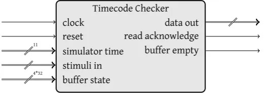
4.2.5 Timecode checker
4.3. SOFTWARE IMPLEMENTATION 31
also copied to a register that is used in the following delta cycles if the sample is still valid. This avoids incorrect consumption of data. The ports of the timecode checker are specified as shown in figure 4.8.
. .Timecode Checker
.clock . .reset . .simulator time . . 11. .
.data out . . ..
.stimuli in .
.. .
.read acknowledge . .buffer empty .
.buffer state .
[image:41.595.139.402.173.265.2]. 4*32. .
Figure 4.8: Timecode checker port specification
As noted in section 3.2.2, the timecode checker delivers data to the system con-troller, which determines the precise moment at which the data is offered to the simulator. This moment is determined using two signals in the state port of the simu-lator, namedprefetch_stimuliandprefetch_stimuli_valid. The first signal identifies the instance that will be simulated after three clock cycles. When the signal is valid (prefetch_stimuli_validbecomes high), the stimuli element for the corresponding identifier should be offered to the stimuli port of the simulator.
If A DUT has multiple external inputs, a shift register must be used to offer data at the correct moment to the simulator. The IIR filter only has a single external input. Therefore, the identifier check and shift register are not implemented.
4.2.6 Output buffer
For analysis of the simulation afterwards, the output of the simulated entities is stored in a FIFO buffer also. The implementation of the output buffer is based on the implementation of the input buffer. The controller extracts the current time from the state of the simulator. It is coupled to the output of the current entity and stored in the buffer. For fast consumption, the entire address space of the buffer is accessible by a GPP, but for data validity, only addresses which have been written may be read. The GPP must prevent this by verifying that the read pointer does not pass the write pointer. The controller of the output buffer prevents that data is writ-ten before being read. The controller can set the interrupt flag at a certain capacity level, to prevent buffer overflow, but this is not implemented.
The output buffer interface is specified as shown in figure 4.9, using the type definitions of listings 4.1 and 4.2.
4.3 Software implementation
The software is intentionally kept basic, as the test case is very basic. This means that several steps, which could be eased with procedures and functions, are left for future implementation and have to be performed manually for now. An exception is made for the initialisation procedure of the bridge with the FPGA, as this will be used often.
. .Output buffer .memory map clock .
.simulator clock .
.reset .
.read address .
. 12. .
.data to ARM . . ..
.buffer state . . .4*32.
.buffer control .
. 32+1. .
.IRQ .
.data from simulator .
.. .
.simulator state .
.. .
[image:42.595.173.462.122.246.2].acknowledge .
Figure 4.9: Output buffer port specification
The structure is initialized in a precompiler directive, which places the memory map at the correct start address. For readability, several portions are divided in an own structure. For example the simulator state and control are specified as shown in listings C.2 and C.3. For more information on the definition of these variables see [33].
In contrast with the hardware implementation, the variables likeread_fromare not yet assembled of record structures. C is byte-oriented, not bit oriented like VHDL.
To verify the behaviour of the memory map in all regions of the addressing space, the hardware implementation returns debugging data at several positions. The mem-ory position of the test registers is specified in listing C.1.
4.3.1 Configure connection
Before the ARM processor can use the connection with the FPGA, the connection must be configured correctly. The functionbridge_initconfigures the interface in 5 steps:
1. Configure (Parallel I/O)PIO clock
2. Enable PIO clock
3. Configure PIO Reset
4. Reset PIO
5. Configure memory controller
a) Configure Setup time b) Configure pulse time
c) Configure total cycle duration d) Configure read/write mode
4.3. SOFTWARE IMPLEMENTATION 33
4.3.2 Test connection
To verify whether the connection has been configured correctly, the test registers that exist in the memory map listing C.1 are examined and compared with the ex-pected value. This is included in the functionbridge_init().
4.3.3 Configure simulation
After initialization of the connection with the FPGA, the simulator is stopped to con-figure the simulation. The number of entities which are used for this simulation are set by issuing the commandENABLEon the address0x300F0300and writing a value to memory address0x300F0304. After enabling a number of entities, links between en-tities are created. A function is created for this purpose which is listed in listing C.4. This function issues several commands according to section 2.3.2:
1. CommandCREATE_LINKSat address0x300F0300
2. Instance address at address0x300F0304
3. Instance reads from at address0x300F0308
4. Instance stimuli mask at address0x300F030C
5. Instance writes to at address0x300F0310
4.3.4 Run simulation
With all settings created, stimuli should be inserted in the stimuli buffer before performing the actual simulation. Stimuli is copied to the an address in the range 0x30000000up to0x30010000, and the write pointer is updated afterwards by writing the new pointer value to address0x300F000C.
CHAPTER
5
Tool evaluation for
Hardware/Software
co-simulation
The design and implementation discussed in chapters 3 and 4 is actually the design of a co-simulation system. Basic ideas of co-simulation are discussed in section 2.2.
Previous work has shown that stimuli generation significantly increases the load on a processor [39]. A PC is equipped with a greater amount of processing power; the amount of processing power available for other tasks is far greater than in the embedded processor. A PC will be used to replace the embedded processor as shown in figure 5.1. Also enhanced stimuli generation is possible. Using a PC also opens up
.
.
. .
.
Stimuli Generation
.
Data Analysis
.
System control
.
Stimuli buffer
.
Simulation
.
Output buffer
[image:45.595.119.417.495.610.2].Computer(MATLAB) .FPGA
Figure 5.1: Co-simulation system structure
extended capabilities to perform data analysis in various tools. Several tools can be used for the connection of a PC to SHILS, which are compared in this chapter.
MATLAB is sometimes already used in initial design stages for algorithm explo-ration and other tests. To be able to reuse previously made test benches (in MAT-LAB), MATLAB is used to generate the stimuli and analyse the output data. Some-what equivalent to the computing capabilities of MATLAB is GNU Octave [18], but
that application is not directly equipped with co-simulation facilities and therefore not discussed in the context of this thesis.
5.1 Requirements
An important aspect is the operating method of SHILS. Implementations so far use a data pushing method to keep the simulator supplied with sufficient stimuli (chap-ter 3, [39]). This method is used to maximize data throughput. The simulator expects data to be ready for it all the time; therefore the synchronization mechanism is im-portant. To reduce communication overhead, it is desirable to send a large quantity of data at the same time to the simulator input buffer. MATLAB is generally used sequentially, but can function perfectly asynchronous.
The current implementation of the SHILS external interface is a MMIO interface (chapter 3). This enables transmission of data via a unified interface. Minimized effort in migration of the interface in both hardware as software towards the new co-simulation system is an advantage.
The tool discussion assumes that MATLAB is used for stimuli generation, and the tool is used to arrange the connection. However, MATLAB can also arrange the connection. It is discussed as an option for this reason.
5.2 Criteria
The tools to connect SHILS with MATLAB are evaluated according to multiple cri-teria. These criteria are based on the aforementioned requirements. In the tool comparison is the interface that will be used to connect SHILS not decided.
Damstra has defined key factors which define a good co-simulation system [16]. These key factors are purely focused on software-based simulation. The key factors of Damstra have been used to formulate the tool evaluation criteria, they are modi-fied to apply to hardware connectivity, effort to use and performance. The criteria have influence on each other and partially overlap.
The criteria are evaluated individually. The majority of the criteria are evaluated using an ideal solution that is best for each specific criterion, resulting in ++, +, o, -, -- or --- to indicate how a specific product relates to the ideal. The ideal for each criterion is discussed below. Criterion 3 and 7 cannot be judged in this manner, they are judged upon available features.
1. Hardware connectivity possible This criterion expresses whether the tool can con-nect with hardware by default. It is desirable that concon-nectivity with hardware can be enabled without great effort. The best case is that connectivity can be automatically arranged/generated.
5.2. CRITERIA 37
3. Supported I/O protocols This criterion concerns the different methods which could be used to connect the tool with hardware. This is closely related with the physical interface used by SHILS, as is must connect with software over this interface too. The evaluation of this criterion only lists the possible protocols, as the comparison of tools is performed independently of the platform used and thus the physical in-terface used.
4. FPGA integration This
![Figure 3.5: Timing diagram based on Rutgers [33]](https://thumb-us.123doks.com/thumbv2/123dok_us/1227040.646931/32.595.165.473.257.471/figure-timing-diagram-based-on-rutgers.webp)