International Journal of Emerging Technology and Advanced Engineering
Website: www.ijetae.com (ISSN 2250-2459,ISO 9001:2008 Certified Journal, Volume 5, Issue 12, December 2015)
163
High Performace Based Single Phase Interleaved Flyback Grid
Tied Inverter for Solar Application
P. Booma Devi
1, P. Saravana kumar
21Assistant Professor/EEE, 2PG Student/EEE, RVS College of Engineering, Dindigul. Abstract-- A high performance based single-phase grid
connected Interleaved fly back converter for Solar application is proposed. The inverter is derived from a boost cascaded along with a line frequency unfolding circuit. Due to its novel operating modes, high efficiency can be achieved. because there is only one switch operating at high frequency at a time, and the converter allows the use of power MOSFET and ultra-fast reverse recovery diode two-phase interleaved inverter is then designed accordingly. The double-carrier modulation method is proposed based on the inverter’s operation mode. Because of this, the carrier for boost mode is stacked on the top ofthe carrier for buck mode, as a result, there is no need to compare the input and output voltage to decide which mode the inverter should operate in. Based on similar concept, three advanced modulation methods are proposed. First method can help further improve the efficiency, and one the second method can help increase the bandwidth and gain, and the last one takes the advantage of both. This can be achieved by three dual-mode double-carrier based SPWM inverters.As a result, the common mode (CM) voltage kept constant during the whole grid period reduces the leakage current significantly. In addition, dead time is not necessary for main power switches at both the high frequency commutation and the grid zero crossing instant. With both step-up and step-down functions, this type of inverter can achieve high efficiency of about 97.4% in a wide range because only one switch operates at the PWM frequency at a time.It is the boost modeinverter in which only one power stage works at high frequency in order to achieve minimum switching loss. The minimum voltage drop of the filtering inductor in the power loop is achieved to reduce the conduction power loss.
Keywords-- Maximum power point tracking, Interleaved Flyback converter, H6 topology, SCR Bridge.
I. INTRODUCTION
With the worsening of the world’s total energy shortage and environmental pollution problems, protecting the energy and the environment becomes the specific major problems for human beings. Thus the development and application of the renewable energy. Differentsystem solarenergy, wind energy, fuel cell, tides and geothermal heat etc., are getting more and more attention. Among them, solar system power will be dominant because of its availability and reliability.
As predicted by [1], the solar will provide the total electricity up to 64% of the total energy by the End of this century. Photovoltaic (PV) power generation system has become one of the main ways to use solar energy. And the renewable energy sources mainly based distributed generation (DG) system is interfaced to the grid through power electronic converters or inverters. Thus developing a photovoltaic grid-connected interleaved inverter system is important for the mitigation of energy and environmental issues.
II. HIGHER EFFICIENCY FOR BOOST CONVERTER
For these single stage grid tied inverters, either a transformer is used for boosting the input voltage or the input voltage will be required to be higher rating the peak of the grid voltage, which is not good for PV application because the solar panel’s characteristics changes all the time. The energy storage needs to be at the front of a single stage inverter, and it is mainly implemented by electrolytic capacitors. The lifetime issue of an electrolytic capacitor is introduced. And the result can be drawn that although the electrolytic capacitors have limited lifetime, it can still be used by applying minimum voltage and current ripple to prolong its lifetime. Because the end of its life doesn’t mean it failed, the electrolytic capacitor can work maximum longer than its estimated lifetime. As the capacitance also has an impact on MPPT efficiency, the maximum capacitance leads to higher MPPT efficiency. After that, a boost-buck converter based inverter is proposed. System operates in either boost or buck mode; thus, it has a wide input voltage range or high efficiency can be achieved. Then, the system analysis of its middle capacitor and CCM/DCM operation condition is presented. Since the common-mode voltage in this flyback inverter is equal to the grid voltage, it changes at line frequency. The leakage current of it is very small even at an extreme case.
III. INTERLEAVED ACTIVE CLAMP FLYBACK DESIGN.
International Journal of Emerging Technology and Advanced Engineering
Website: www.ijetae.com (ISSN 2250-2459,ISO 9001:2008 Certified Journal, Volume 5, Issue 12, December 2015)
164
Flyback converters are generally used in low power system and Step-down applications, system less than a couple maximum watts define as that have a grid side low output current. A forward converter can also step up the PV panel voltage and provide galvanic isolation. When comparing the operation of two topologies, the flyback converter requires fewer components as there is no freewheeling diode rectified on the output or the need for an output inductor; this is why the interleaved clamp flyback topology was selected. The leakage spike is a system clamped by the clamping capacitors (Cclamp), and then the created energy is stored in the clamping capacitors. If correctly implemented, the active clamp circuit also provides Zero Voltage drop switching on the flyback MOSFET, which reduces the switching losses and improves overall efficiency.
Figure1: Active clamp flyback converter
IV. PROPOSED BUCK-BOOST BASED ON PVINVERTER
A boost-buck type of circuit dc-dc converter is proposed as the first stage with regulatedoutput inductor current, and a full-bridge converter unfolding circuit with 50- or 60-Hz line frequency is applied to the dc-ac stage, which will unfolding clamp the rectified sinusoid current regulated by the dc-ac stage into a pure sinusoidal current, as shown in Figure 3.
Since the circuit runs either in boost or buck mode, its first stage can be very efficient if the low conduction voltage drop switching power MOSFET and ultra-fast reverse recovery diode are used. For the second stage, because the unfolding circuit only operates at the no loss line frequency and switches at zero voltage and current, the switching loss can be rejected. The only loss is due to the conduction voltage drop, which can be minimized with the use of low on drop power devices, such as thyristor or slow-speed IGBT. In this version, IGBT is used in the unfolding circuit because it can be easily operate turned on and off with gating control. Since only the boost dc-dc converter or buck dc-dc converter operates with in a high frequency switching all the time in the proposed system, the efficiency is improved. And because there is only one high operating frequency power processing stage in this complete PCS, the reliability can be greatly enhanced. Other than these, the analysis of middlecapacitor and CCM/DCM operation condition is also presented.
International Journal of Emerging Technology and Advanced Engineering
Website: www.ijetae.com (ISSN 2250-2459,ISO 9001:2008 Certified Journal, Volume 5, Issue 12, December 2015)
165
Figure3: Buck-boost based PV inverter
V. BOUNDARY MODE ANALYSIS
As mentioned before, during the buck mode, the input current can be treated as the input filter’s inductor’s current, whose ripple is much reduced from the filtering effect. Similarly, during the boost mode, the output current can be treated as the output circuit filters and inductor’s current, whose ripple is also much mitigated. Due to this dual filter effect, the DCM mode operation is very rare in the proposed circuit. In fact, the circuit is always running in continuous current mode (CCM) for input current in buck mode and output current in boost mode. That also indicates that discontinuous current mode (DCM) or boundary mode can happen only in output current in buck mode and input current in boost mode. Then it can be analyzed as a normal buck and boost converter. The boundary condition can be derived based on the input current ripple for boost mode and output current ripple for buck mode as below figure.
Figure4: Boundary power condition for Input current with different input voltage.
Figure5: Boundary power condition for output current with different input voltage.
VI. LEAKAGE CURRENT ANALYSIS
The reported that the capacitance between the point of contact and a singlePV module has been calculated to range between 100 – 400 pF. The capacitance depends on weather conditions, and in the worst case as rainy days, the capacitance can be as high as 80 nF/kW. Because of there is no isolation between the input and output without a transformer, the transformer less grid tied inverter needs to consider the leakage current issue asShown in Figure 6..
International Journal of Emerging Technology and Advanced Engineering
Website: www.ijetae.com (ISSN 2250-2459,ISO 9001:2008 Certified Journal, Volume 5, Issue 12, December 2015)
166
Table 1: leakage current and corresponding decondition time.Because of this safety issue, the leakage current should be as small as possible for transformerless inverter. Many literatures analyzed the leakage current in transformerless grid-connected inverter. For the proposed topology, the negative terminal“O” of solar modules is set as the reference point, and the middle points of the bridge legs are set as phase and neutral for the output terminals. Since vgrid is not constant but sinusoidal with 60 Hz, there is a small line frequency leakage current in the proposed inverter. For a 2.5 kW system, the capacitance between the PV modules and the ground CPV would as high as 200nF. The simulated leakage current in this extreme case is shown in Figure 7. It shows that even in this extreme case, the leakage current is still far below the standard.
VII.VII CONTROL OF THE BOOST –BUCK MODE PV INVERTER
During buck mode, inductor current can be treated as normal buck converter’s output inductor current which can be easily controlled. However, it is critical to control inductor current in boost mode because the control target in this mode its output circuit filters’s inductor current. Thus, the compensator for boost mode needs to be designed first and then applies it to buck mode. In practice, if the boost mode is stable and well controlled, buck mode will be stable and well controlled as well. The loop gains of boost mode at different operating points are shown in Figure 3.13. It clearly shows that the RHP zero and double pole make 270° phase delay, which makes it difficult to be compensated. Thus, the compensated crossover frequency needs to be before double-pole’s frequency of the boost mode and to insure that the peak Q value is lower than 0dB. In order to have a compensator that is good for every operation point, the compensator design is system based on the worst conditions, which is defined as a condition with highest Qpkand the earliestphase drop.
In our case, worst condition happens when input voltage is the lowest defined value 200 V and output voltage is the peak voltage of the grid 340 V.
Figure7: Analog control for smooth
Figure8: Digital control for smooth
In order to achieve smooth waveform in transition between boost to buck modes, an offset of the sawtooth carrier right on the top of the buck mode PWM modulator needs to be applied to boost mode as shown in Figure. The high gain of buck mode can be realized by reducing the carrier magnitude for buck mode as described in 4.2. As a result, universal control for both modes can be achieved. If a digital signal processor (DSP) is employed as a controller, smooth transition between the two modes can be achieved in different ways by taking advantage of flexible algorithm implementation. For example, in our test-bed system, the signal after compensator is deducted by a unit as shown in Figure.in order to achieve smooth transition between the two modes.
International Journal of Emerging Technology and Advanced Engineering
Website: www.ijetae.com (ISSN 2250-2459,ISO 9001:2008 Certified Journal, Volume 5, Issue 12, December 2015)
167
Grid-Tie Converter Controller
To send the energy to the grid, the following controller algorithm must be realized in this system:
1. Phase-locked loop (PLL) controller. The PLL
controller logic is used to synchronize with the grid
Voltage, which can provide a reference system phase to the current controller.
2. Grid-tie current controller, the current controller
can ensure the output current is a sine
Wave signal and trace the current reference to balance the input power and the output power.
3. Maximum power point tracking, The MPPT is
used to track the panel into a maximum Power output stage.
Figure9: the controller structure
The phase error detection. Detect the phase error between the reference and the sine wave out. This detection is done in 1-ms task A0. The PLL controller. Close loop controller, the controller is executed in 1-ms task A0.The Sine generator. Systemgenerate the sine wave according to the frequency and sample time; this is done in the ISR.Equation of a load sharing transfer function,
Ipv1(s) = Gd, ipv1(s) Xd(s) (1.1)
Ipv2(s) = Gd, ipv2(s) Xd(s) (1.2) Let the error between the currents be equal to ΔI. Therefore, the currents can be seen as follows in Equation of a load sharing current error,
Ipv1(s) = Ipv2(s) = I = (Gd, ipv1(s) –
Gd, ipv2(s)) X d(s) (1.3)
The goal is to make both the currents the same (i.e.,
Make Ipv1as Ipv1(s) – ΔI/2andIpv2asIpv2(s) + Δ I/2)
byincluding correction factors of ±Δd.
Equation of load sharing the correction factor,
Ipv1(s)-I/2 = Gd, ipv1(s) X (d(s) - d(s)) (1.4)
Ipv2(s) + I/2 = Gd,ipv2(s) X (d(s) + d(s)) (1.5) Equation of a load sharing current,
I = (Gd, ipv2-Gd, ipv1) d(s) + (Gd, ipv2+Gd ipv1)
d(s) (1.6)
Assuming Gdipv2 ≈ Gdipv1 ≈Gdipv
ΔI(s) = 2Gdipv(s) Δd(s)
Figure10: current control loop
Using the system of PI controller, the controller calculation frequency is 22 kHz. The open loop bandwidth must be set to 1 to 2 kHz. Figure 10 indicates that the feedback of the close loop must be the primary side current ip, but in the real system it is the curve middle point current when Q1 is turned on in the real system. If the converter is working of a continuous mode, the relationship between the system of primary feedback and the Secondary average current is, to get a sine wave output current, the secondary average current must be a sine wave signal therefore, it is necessary to modify the output feedback current to the following model.
International Journal of Emerging Technology and Advanced Engineering
Website: www.ijetae.com (ISSN 2250-2459,ISO 9001:2008 Certified Journal, Volume 5, Issue 12, December 2015)
168
International Journal of Emerging Technology and Advanced Engineering
Website: www.ijetae.com (ISSN 2250-2459,ISO 9001:2008 Certified Journal, Volume 5, Issue 12, December 2015)
169
International Journal of Emerging Technology and Advanced Engineering
Website: www.ijetae.com (ISSN 2250-2459,ISO 9001:2008 Certified Journal, Volume 5, Issue 12, December 2015)
170
GRID And PLL Simulation
The PLL is integral to the operation of the inverter in that everything about DC/AC conversion is managed in sync with the AC line. All state management is synchronized to the line. All inversion-related control operations are synchronized to the line. The only item that is not directly synchronized to the line (although it could be) is the ripple cancellation control algorithm. The PLL is operated slightly differently than that of other PLLs for this design. A line cycle is divided into 1024 slices, or 512 slices per half-sine. And the number of slices does not change. However, the distance between each slice is allowed to change. One key advantage is that the sine
reference information is always the same.
Simulation Results:
Figure: average flyback input currents
Figure: current error
The load sharing local load and grid to control loop constantly monitors the error between the input currents of the converters and will minimize this error. the dynamically adjusting the duty ratio of each of the converters by the addition/subtraction of a small common correction factor value depending on the sign of the error.
International Journal of Emerging Technology and Advanced Engineering
Website: www.ijetae.com (ISSN 2250-2459,ISO 9001:2008 Certified Journal, Volume 5, Issue 12, December 2015)
171
[image:9.612.333.550.133.376.2] [image:9.612.51.287.322.511.2]The main role of the feed-forward compensator in the solar inverter system is to provide the steady state duty ratio, “D(t)”, to the sharing system, thereby allowing the compensator value error system. The feed-forwardNetwork will help to compensator to reject the disturbances caused by fluctuations in both the solar panel input voltage, and the output voltage of grid voltage. The load resistance has been included in the term, Rf, as the filter inductor and DCR is in series to the load resistance in the AC-equivalent circuit. From the open-loop bode plot, it can be observed that both of gain margin and phase margin of the system are low, and thus, the system inherently has a poor relative stability. Additionally, it is mainly observed that the switching frequency ripples attenuation needs improvement and that the system gain at the required system operating frequency (100/120 Hz) is very low.
[image:9.612.48.289.532.693.2]Figure: grid current and current reference
Figure: grid voltage
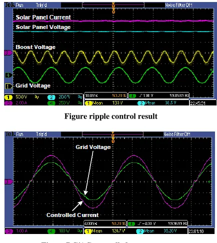
Figure ripple control result
Figure DC/AC controlled output current
Therefore, for the MPPT loop, and the current control loop appears as a unity gain system with zero or minimal phase error. The current loop modulates the Converter current into a rectified signal is a sine wave output. The MOSFETfull-bridge unfolds this rectified current into an alternating current to be delivered to the grid. The current loop bandwidth can be improved through the use of a gain feed forward compensator. The steady-state duty cycle can be dynamically computed using the measured PV panel voltage and AC grid voltage. While the feed-forward compensator supplies the steady-state modulation, the current control loop takes the account of dynamic
variations and modulates the controlled current
accordingly. The following sections discuss the function calculation mathematical modeling of the solar inverter system to obtain the transfer functions of output to control input and control output to disturbance inputs of the system.
IX. CONCLUSION
International Journal of Emerging Technology and Advanced Engineering
Website: www.ijetae.com (ISSN 2250-2459,ISO 9001:2008 Certified Journal, Volume 5, Issue 12, December 2015)
172
Along with that, three advanced control methods are also proposed Based on the operation mode concept, many topologies can be proposed. If any inverter is working based on buck converter’s concept, it can be integrated with boost part. As a result, the new inverter won’t have the limitation on its input voltage, which means the input voltage doesn’t need to be higher than the peak ofthe output ac voltage. In this way, the input voltage range could be widened. The topologies that lower switching losses and improve overall system efficiency, High efficiency was achieved by implementing a novel interleaved active-clamp flyback topology with Zero Voltage Switching (ZVS).
X. FUTURE WORKS
1) When the grid is abnormal, the PV inverter needs to disconnect from the grid. A control scheme needs to be developed and further investigated to make the inverter to operate between grid-tied mode and islanding mode. 2) Although the three dual-mode double-carrier based
Switch pulse width modulation inverters are proposed and their efficiency analysis has been provided, some more experiments should be conducted and their actual efficiency should be compared.
3) Other types of dual-mode double-carrier based Switch pulse width modulation inverters can be
Investigated, such as boost along with HERIC (Highly Efficiency and Reliable Inverter Concept) inverter. 4) For boost-FB (Full Bridge) and boost-DB (Dual Buck)
inverter, other modulation methods could be considered to eliminating their leakage currents, such as bipolar PWM modulation method.
REFERENCES
[1] German Advisory Council on Global Change WBGU Berlin 2003 www.wbgu.de; Renewable Energy Policy Network for the 21st Century, Renewables, Global Status Report 2006.
[2] J.-S. Lai, “Power conditioning systems for renewable energies,” in InternationalConference on Electrical Machines and Systems, ICEMS 07, pp. 209-218, Oct.2007.
[3] Y.T. Tan, D.S. Kirschen, and N. Jenkins, “A model of PV generation suitable forstability analysis,” IEEE Trans. Energy Convers., vol. 19, no. 4, pp. 748-755, Dec 2004.
[4] S. Duryea, S. Islam, and W. Lawrence, “A battery management system for standalonephotovoltaic energy systems,” IEEE Industry Applications Magazine, vol. 7, no. 3, pp. 67–72, Jun. 2001. [5] Strong, Steven (June 9, 2010 (last update)). "Building Integrated
Photovoltaics(BIPV)". Whole Building Design Guide. Retrieved 2011-07-26.
[6] Bangyin Liu, Shanxu Duan, Tao Cai, “Photovoltaic DC-Building-Module-BasedBIPV System-Concept and Design Considerations,” IEEE Trans. Power Electron, Vol. 26, No. 5, pp. 1418 – 1429, 2011. [7] H Chiu; Y Lo; C Yao; S Cheng, “Design and Implementation of a
Photovoltaic High-Intensity-Discharge Street Lighting System,” IEEE Transactions on PowerElectronics, vol.26, no.12, pp.3464-3471, Dec. 2011
[8] J. P. Benner and L. Kazmerski, “Photovoltaics gaining greater visibility,” IEEESpectr., vol. 29, no. 9, pp. 34–42, Sep. 1999. [9] R. Billinton, and R. Karki, “Capacity expansion of small isolated
power systemsusing PV and wind energy,” IEEE Trans. Power Syst., vol. 16, no. 4, pp. 892-897,Nov 2001.
[10] J. Selvarajand, N. A. Rahim “A novel pulse width modulation for grid-connected multilevel inverter,” Journal of renewable and Sustainable energy 1,053102, 2009.
[11] B. Yang, W. Li, Y. Gu, W. Cui, and X. He, “Improved transformerless inverter with common-mode leakage current elimination for a photovoltaicgrid-connected power system,” IEEE Trans. Power Electron., vol. 27, no. 2, pp. 752–762, Feb. 2012. [12] R. Gonzalez, E. Gubia,J. Lopez, and L.Marroyo, “Transformerless
single phase multilevel-based photovoltaic inverter,” IEEE Trans. Ind. Electron., vol. 55, no. 7, pp. 2694–2702, Jul. 2008.
[13] H. Xiao and S. Xie, “Transformerless split inductor neutral point clamped three-level PV grid-connected inverter,” IEEE Trans. Power Electron.,vol. 27, no. 4, pp. 1799–1808, Apr. 2012.
[14] L. Zhang, K. Sun, L. Feng, H.Wu, and Y. Xing, “A family of neutral point clamped full-bridge topologies for transformerless photovoltaic grid-tied inverters,” IEEE Trans. Power Electron., vol. 28, no. 2, pp. 730–739, Feb. 2012.