International Journal of Emerging Technology and Advanced Engineering
Website: www.ijetae.com (ISSN 2250-2459,ISO 9001:2008 Certified Journal, Volume 3, Issue 12, December 2013)
558
Design and Implementation of Modified Charge Pump for
Phase Locked Loop
M. Mano
1, G. Selva Priya
2, K. RekhaSwathi Sri
3 1,2,3PG Scholar, Department of ECE,Bannari Amman Institute of Technology
Abstract--A PLL is a closed loop system that locks the phase of an output signal to an input reference signal. The term “lock” refers to a constant or zero phase difference between two signals. The components of PLL are the Phase Frequency Detector (PFD), the charge pump (CP), the low pass filter (LPF), and the voltage controlled oscillator (VCO). In which the charge pump has been modified in order to overcome the leakage current. Hence power consumption is reduced through the modified structure. All the components of PLL are designed and integrated. All the components are designed in 0.35µm CMOS technology. Once the locked state of PLL is achieved the output of all the components of PLL are constant.
Keywords--PLL components, modified charge pump, Leakage current, CMOS
I. INTRODUCTION
A PLL is a closed loop frequency system that locks the phase of the outputsignal to the reference signal. The term “lock” refers to a constant or zero phase difference between two signals[1]. PLL are primarily used for communication system. The main application of the PLL includes AM Radio receivers, Frequency Demodulators, Dividers, Multipliers and Frequency Synthesizer. Recent advances in IC design techniques have led to an increased use of the PLL as it has become more reliable and economical [2].The signal from the feedback path, ffb, is compared to the input reference signal, fref, until the
two signals are locked. If the phase is unmatched, this is called the unlocked state, and the signal is sent to each component in the loop to correct the phase difference[3]. The major components of PLL are Phase Frequency
Detector(PFD), Charge Pump(CP), Low Pass
Filter(LPF), Voltage controlled Oscillator(VCO) and Frequency Divider(FD). The input to the PLL is a reference frequency depending upon the user. The Phase Frequency Detector(PFD), compares the reference signal, fref and thefeedback path, ffband generates an error signal
[4].
Based upon the error signal the Charge Pump (CP) either increases or decreases the charge to the low pass filter(LPF). This amount of charge either speeds up or slows down the VCO. The loop continues in this process until the phase difference between fref and ffb is zero or
constant this is the locked mode [6,7].
Figure: 1.1 Basic Phase Locked Loop
II. FUNDAMENTALS
A Phase Locked Loop or a PLL is a feedback control circuit. As the name suggests, the phase locked loop operates by trying to lock to the phase of a very accurate input signal through the use of its negative feedback path. A basic form of a PLL consists of four fundamental functional blocks namely
A Phase Detector (PD)
Charge Pump (CP)
A Loop Filter (LF)
A voltage controlled oscillator (VCO)
Frequency Divider(FD)
International Journal of Emerging Technology and Advanced Engineering
Website: www.ijetae.com (ISSN 2250-2459,ISO 9001:2008 Certified Journal, Volume 3, Issue 12, December 2013)
559
III. PLLCOMPONENTS
A.Phase Frequency Detector
The Phase Frequency Detector(PFD), is used to detect the phase difference between the input reference signal and the feedback signal. It provides an error signal based upon the phase difference.The PFD design uses two flip flops with reset features as shown in Figure 4.3The inputs to the two clocks are the reference and feedback signals (frand f0). The D inputs are connected to VDD
always remaining high. The outputs are either “UP” or “DN” pulses. These outputs are both connected to an AND gate to the reset of the D-FF’s. When both UP and DN are high, the output through the AND gate is high, which resets the flip flops. Thus, both signals cannot be high at the same time. This means that the output of the PFD is either an up or down pulse but not both. The difference in phase is measured by whichever rising edge occurs first.
Figure: 1.2PFD Implementation Using D Flip Flop
B.Charge Pump
Charge Pump is used to produce a charge proportional to the error signal. The function of a charge pump and loop filter is to take the digital UP and DOWN pulses from the PFD and convert them into an analog control voltage, Vcntrl.The charge pump consists of two switched current sources that are used to pump charge into or out of loop filter. Whenever the reference signal leads the feedback signal the PFD detects the rising edge on the reference signal and produces an up signal. This up signal from the PFD turns on the up switch in the charge pump and injects current into the loop filter. Whenever the feedback signal leads the reference signal the PFD detects the rising edge on the feedback signal and produces an Down signal. This Down signal from the PFD turns on the Down switch in the charge pump and sink current from the loop filter. The current through the UP switch, Iup, and the current through the down switch,
Idown, need to be equal in order to avoid any current
mismatch. The minimum charge pump current is limited by the switching speed requirements.
Figure: 1.3 Charge Pump
Figure:1.4 Charge Pump Output
Figure: 1.5 Modified Charge Pump
International Journal of Emerging Technology and Advanced Engineering
Website: www.ijetae.com (ISSN 2250-2459,ISO 9001:2008 Certified Journal, Volume 3, Issue 12, December 2013)
560
The Conventional charge pump and the modified charge pump output are shown. The modified charge pump provides an exact current match between the UP and Down signal. Hence it reduces power consumption and power dissipation in the system. Hence the modified charge pump design can be implemented for low power PLL.
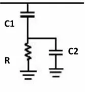
C.Loop Filter
Loop filter is an important component in PLL, as it affects and determines the loop stability. It also provides the necessary control voltage that is required to adjust the frequency of the VCO. Figure 1.7 shows the RC network, which includes a resistor in series with the filter capacitor. Each time the charge pump drives the R and C1 combination, a current is injected into the filter, and the control voltage experiences a jump. To suppress this effect, a second capacitor (C2) is added in parallel with the resistor. This results in a 3rd order LPF circuit shown below in Figure 1.7.
Figure: 1.7 3rd order LPF circuit
The newly added capacitance, C2, should be about1/10 of the C1. This is a common design practice used when designing the loop filter for a PLL. This circuit results in the following transfer function Z(s):
Z(s) = R + (1.1)
Because C2 is such a small value, it can be ignored for simplicity in the calculations. The loop becomes more stable as R increases. However, when R gets really large, the stability degrades.
D.Voltage Controlled Oscillator
An important circuit used in modern communication system is Voltage Controlled Oscillator (VCO). The VCO’s output is an AC Waveform whose frequency depends upon the input voltage. In today’s wireless communication systems, a greater maximum frequency range is required by the VCO’s. The VCO used is Ring Oscillator, it consists of odd number of open loop inverting amplifiers in a feedback loop. The simplest type of amplifier that can be used is a simple digital inverter, as shown in Figure 1.8. The circuit will oscillate and for each half-period, the signal will propagate around the loop with an inversion.
This change will propagate through all three inverters in a time of T/2, at which time the output of the first inverter will change to 0 and after an additional time of T/2 the first inverter’s output will change back to 1. Assuming each inverter has a delay of and that there are N inverters.
[image:3.595.122.206.370.460.2]Figure 1.8: 3 Stage Ring Oscillator
Figure 1.9: Stage Ring Oscillator
Figure1.10: 5 Stage Ring Oscillator Output
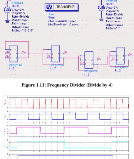
E.Frequency Divider
A clock frequency division can be implemented, with a digital logic resetting the counter after a number of input clock cycles equal to the division ratio. The main drawback of this implementation is maximum frequency of operation due to digital logic with which the counter implemented. A frequency divider operates up to few GHz. This type of frequency divider is of low power consumption and programmable by changing the resetting logic. For higher frequency division, an analog solution is considered.
In frequency divider the D type flip flop can be connected together to form a binary divider. Here the inverter output terminal Q is connected directly back to the data input terminal D giving the device feedback.
R
C2
International Journal of Emerging Technology and Advanced Engineering
Website: www.ijetae.com (ISSN 2250-2459,ISO 9001:2008 Certified Journal, Volume 3, Issue 12, December 2013)
561
The output signal at Q has a frequency that are exactly one half that of the input clock frequency. In which other words the circuit produces frequency division as it now divides the input frequency by a factor of two. For divide by 4 frequency divider we can connect together in series, two D type flip flops the initial input frequency will be divide by 2 by the first flip flop and then divide by 2 again by the second flip flop, giving an output frequency which has effectively been divided four times, then its output frequency becomes one quarter value of the original clock frequency. Each time another flip flop we add, the output clock frequency is halved again and so on, giving an output frequencyof 2n where “n” is the number of flip flops used in the sequence.
[image:4.595.339.525.226.335.2]Figure 1.11: Frequency Divider (Divide by 4)
Figure 1.12: Frequency Divider (Divide by 4) Output
IV. PLLIMPLEMENTATION
The components are designed for the given specification, all the components are integrated together to form the PLL. The design specification is given in Table 1.1. The PFD compares the input reference signal and the feedback signal and produces an error signal which produces an UP and Down signal. If UP signal is produced the Charge is injected to Loop Filter else it sink Current from Loop Filter.
[image:4.595.51.279.302.445.2]The charge from the CP is used to correct the variation in the VCO. If there is a difference in the PFD then it is in Unlocked State the loop continues until the PLL achieves Locked state. Once locked state is achieved then the output of all the components of PLL are almost constant. Thus PLL locks a particular frequency range and produces a constant frequency as output.
Table I PLL Specifications
Damping Ratio ζ=1
C1 200Pf
Icp 50 A
fref 100MHz
fout 400MHz
As displayed in Table I, the output frequency must be four times that of the reference frequency. The reason for this is that the VCO operates ideally (curve is linear) in the 400MHz range. However, that frequency is too high to be a reference frequency, as fref is usually much
less than fout. This is because in the real world, crystal
oscillators that are high in frequency are very expensive; so a smaller reference frequency is used. Thus, in order to get a higher output frequency, a divider must be put in the feedback path. For this case, a divider of N=4 was necessary to achieve the above reference and output frequency specifications.
Figure 1.13: PLL Output
V. CONCLUSION
[image:4.595.51.277.309.577.2] [image:4.595.336.524.484.658.2]International Journal of Emerging Technology and Advanced Engineering
Website: www.ijetae.com (ISSN 2250-2459,ISO 9001:2008 Certified Journal, Volume 3, Issue 12, December 2013)
562
The individual components such as Phase Frequency Detector (PFD), Charge Pump (CP), Voltage Controlled Oscillator (VCO) and Frequency Divider of Phase Locked Loop is designed and simulated. In which the Charge Pump is modified to achieve low leakage current and to reduce power consumption.
REFERENCES
[1] Long Thanh Bui • Tran-ThuyenChau - “A low phase noise PLL
using Vackar VCO and a wide-locking range tunable divider for V-band signal generation in 65-nm CMOS” Analog IntegrCirc Sig Process (2013) 76:91–102 – SPRINGER.
[2] Changhua Cao et al., “A 50-GHz Phase-Locked Loop in 0.13 m
CMOS” IEEE JOURNAL OF SOLID-STATE CIRCUITS, VOL. 42, NO. 8, AUGUST 2007.
[3] Vahideh Sadat Sadeghi et al., “A new fast locking charge pump PLL: analysis and design” Analog IntegrCirc Sig Process (2013) 74:569–575 – SPRINGER.
[4] Mehdi Kiani et al., “Low voltage low noise open loop automatic
amplitude control for voltage-controlled oscillators” Analog IntegrCirc Sig Process (2010) 62:319–325 – SPRINGER.
[5] Kun-Seok Lee et al.,“Phase Frequency Detectors for Fast
Frequency Acquisition in Zero-dead-zone CPPLLs for Mobile Communication Systems”.
[6] SijieZheng and Lili He* “The Mixed-Signal Design of PLL with
CMOS Technology” Department of Electrical Engineering San Jose State University.
[7] Tai Nghia Nguyen and Jong-WookLee “Low Phase Noise
Differential Vackar VCO in 0.18 m CMOS Technology” IEEE MICROWAVE AND WIRELESS COMPONENTS LETTERS, VOL. 20, NO. 2, FEBRUARY 2010.
[8] Woogeun Rhee “DESIGN OF HIGH-PERFORMANCE CMOS
CHARGE PUMPS IN PHASE-LOCKED LOOPS” Conexant Systems, Inc.*
[9] Scott E. Meninger,Perrott, “A 1-MHZ Bandwidth 3.6-GHz 0.18
m CMOS Fractional-N Synthesizer Utilizing a Hybrid PFD/DAC Structure for Reduced Broadband Phase Noise” IEEE JOURNAL OF SOLID-STATE CIRCUITS, VOL. 41, NO. 4, APRIL 2006.
[10] Jae-Shin Lee et al., “Charge pump with perfect current matching
characteristics in phase-locked loops” ELECTRONICS LETTERS 9th November 2000 Vol.36 N0.23.
[11] Yanping Ding et al., “A 21-GHz 8-Modulus Prescaler and a
20-GHz Phase-Locked Loop Fabricated in 130-nm CMOS” IEEE JOURNAL OF SOLID-STATE CIRCUITS, VOL. 42, NO. 6, JUNE 2007.
[12] Jeffrey S. Pattavina - Charge-Pump Phase-Locked Loop--A
Tutorial.
[13] High Frequency VCO Design and Schematics
-http://www.qsl.net/va3iul/.
[14] Allen and Holberg - CMOS Analog Circuit Design.