Design and Analysis of Dual Edge Triggered (DET)
Flip-Flops Using Multiple C-Elements
K.V.Lalitha1, T.N.L.Surekha2 1
Assistant Professor, Department of ECE Godavari Institute of engineering and technology AP, RJY 2
PG Scholar, Department of (VLSI and EMBEDDED Systems) Godavari Institute of Engineering and Technology, AP RJY
Abstract: Design of Dual-edge triggered (DET) flip-flops that exhibit unique circuit behavior owing to the use of C-elements. Five novel DET flip-flops are presented including two high-performance designs and designs that improve upon common Latch-MUX DET flip-flops so that none of their internal circuit nodes follow changes in the input signal. A common characteristic of the presented flip-flops is their low energy dissipation due to glitches at the input .Here by the designs are constructed on using pass transistors an another one is transmission gate logic. The presented analysis estimates the area and speed. These DET flip-flops are compared to existing DET flip-flip-flops using simulation in a high performance 180 nm CMOS technology and are shown to have superior characteristics such as power and power-delay product (PDP) for a range of switching activities, by using MICROWIND/DSCH 180 nm technology and simulation results obtained by using HSPICE 180 nm technology. The simulation results demonstrate that the proposed circuits are superior in terms of speed, power consumption and transistor count with respect to other designs.
Keywords:Dual-edge triggered (DET), Low power, and High performance.
I. INTRODUCTION
DUAL EDGE triggered (DET) flip-flops achieve the same data rate as single edge triggered (SET) flip-flops at half the clock frequency, which can lead to reduced power dissipation of synchronous logic circuits [2], [3]. The power savings possible using double edge triggered (DET), instead of, conventional single edge triggered (SET) flip-flops. The cost of this reduction is higher circuit complexity of DET flip-flops which usually have more transistors and more internal nodes than SET flip-flops. A common DET flip-flop design called the Latch-MUX DET flip-flop [2], [10] has two input latches multiplexed to one output. The two latches are level-triggered by opposite clock levels so that there is always a transparent latch that follows every change at the input. As a result of this transparency, glitches at the input have an adverse effect on the flip-flop’s power dissipation. It was estimated in [2] that Latch MUX DET flip-flops dissipate less power than SET flip-flops only when glitches are rare. Other DET flip-flop designs include pulsed DET flip-flops [2], [4], [5]. Generally, a pulsed DET flip- flop works by making its output latch transparent to the input signal after every clock edge for a short time interval that is sufficient to reliably latch the input value. Power dissipation of these flip-flops is less dependent on input signal transitions in between the clock edges at the cost of increased power dissipation due to clock activity.
[image:2.612.202.432.552.694.2]
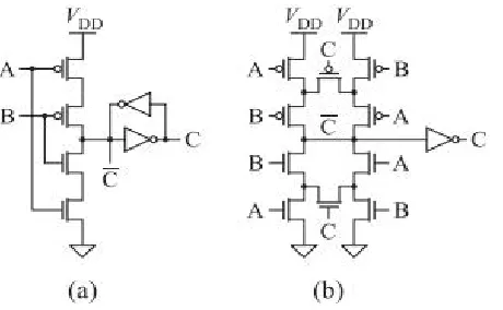
This paper presents novel static DET flip-flop designs that use C-elements. The paper consists of five sections. Section II presents five novel DET designs including the low-glitch-power LG_C flop, implicit-pulsed IP_C flop, floating-node FN_C flip-flop, and two high-performance conditional-toggle CT_C and CTF_C flip-flops. Simulation setup and the comparison methodology that is used to compare the presented flip-flops against each other and against six previously reported DET flip-flop designs.. A C-element, introduced in [6], is normally a three-terminal device with two inputs and one output. When all of its inputs are the same, the output switches to the value of the inputs; when the inputs are not the same, the previous output value is preserved. This device acts as a latch which can be set and reset with appropriate combinations of signal levels at the input. The two transistor-level implementations of C-elements that are used in this paper are shown in Fig. 1. Other implementations have been considered but have not been found to improve on performance, power, or circuit size when compared to the implementations in Fig. 1. C-elements and variations of their circuit topologies are the building blocks of the novel DET flip- flops presented below.
II. PREVIOUS WORKS EXISTING METHOD
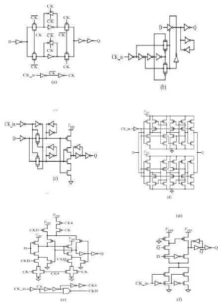
Extensive simulations have been performed to compare the five presented DET flip-flops against each other and also against six previously reported DET flip-flop designs. Two versions of the novel FN_C flip-flop have been considered: The version presented in Fig. 10 and the version with the symmetric C-element of Fig. 1(b) replacing the weak-feedback output C-element. The latter version is denoted as FN_C (sym) in the comparison. For a fair comparison, all flip-flops include input, output, and clock buffering. Transistor-level schematic diagrams of the six previously reported DET flip-flop designs that are considered in this paper for comparison. The designs are as follows:
1) LM, described in [10], is a variant of a common Latch MUX DET design.
2) b) EP is a variant of the common Explicit-Pulsed DET flip- flop that was introduced in [5].
3) c) LM_C is a Latch-MUX design, introduced in [8], that uses a C-element at the output to perform the function of a MUX.
4) d) TSP, presented in [11], is the True-Single-Phase Clock DET flip-flop design that follows the Latch-MUX approach but does not use the inverted clock signal.
5) e) CP, introduced in [2], is the Conditional Precharge DET flip-flop. f) IP, described in [4], is the Implicit-Pulsed DET flip-flop.
The flip-flops were implemented in the 180nm CMOS technology. Implementations were optimized for minimum energy-delay product. For the optimization step, the delay metric was the maximum CK-Q delay because it is straightforward to measure. Optimizations were performed by the simulation tool in an automated fashion: The tool varied transistor sizes within the specified bounds and chose the best sizes for each flip-flop after a number of iterations. The search bounds were chosen so that resultant designs would meet recommended design rules most of the time. Weak transistors were allowed to use minimum width rather than the recommended minimum width as it would otherwise result in poor circuit performance.
Simulations were performed on schematic designs. Conservative estimates of layout parasitics were included in the simulation models at both the optimization and final simulation stages. These estimates were provided by one of the features of the design kit: The kit can automatically include its own estimation of the RC parasitic interconnect network into schematic simulation models. Parasitic extraction and post layout simulations were also performed on selected designs and were compared to schematic simulations that used automatic estimation of parasitics. Post-layout simulations showed that the kit’s estimates for small designs are often conservative and that compact circuits often perform slightly faster in post-layout simulations than in schematic simulations with the automatic parasitic network estimation turned on.
Fig. 2. Transistor-level schematic diagrams of the six previous DET flip-flop designs that are considered in this paper for comparison with the presented novel DET flip-flops. All circuits include input, output, and clock buffering. The flip-flops are (a)
The CV is also known as the relative standard deviation (RSD) which is defined as the ratio between standard deviation (SD) and mean. In this technology, simulation models make somewhat conservative assumptions about sources of variation when performing Monte Carlo analysis on schematic designs. Variations in physical implementations are expected to be lower than the ones reported from these simulations.
III. PROPOSED METHOD
We propose two different designs of DET Flip-Flops
1) One Design construct in Pass-Transistors logic.
2) Another Design construct in Transmission gate logic.
A. New Circuit Design using Pass-Transistors logic.
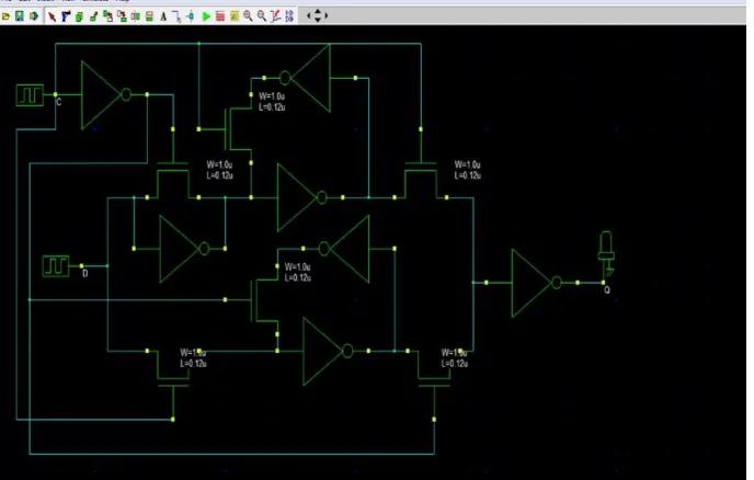
In this flip flop has 20 transistors. The flip-flop shown in Fig3:,structure having two data paths. The upper data path consists of a Single Edge Triggered flip-flop implemented using pass transistors. This works on positive edge. The lower data path consists of a negative edge triggered flip-flop implemented using pass transistors. When positive edge clock pulse is applied then the D input transmitted in upper data path this one construct by using pass transistor logic. This flip-flop operation divided into two cases i.e., When clock positive edge is applied to the circuit then the input applied to both the paths but input data flows through upper data path through data transfer through few inverters and nmos transistors but any edge pulse ‘ l5’ input is zero output ‘Q’ gets at output of ‘ l5’ inverter.
When clock negative edge is applied to the circuit then the input applied to both the paths but input data flows through lower data path through data transfer through few inverters and nmos. In this case also input of ‘ l5 ‘is zero then output directly get one but this operation explain in idle case, in practical case we can get some power consumption appear at output side due to switching transaction and some leakage powers. In this method DET flip-flop consists of 20 transistors and also power consumption is little bit large compare to previous methods.
Fig: 3 DET Flip-Flop
B. New Circuit Design using Transmission gate logic.
So when focus on area for designing DET flip-flop. This one construct in transmission gate logic. By using this logic we can reduce some power consumption and also reduce to area why because in this method DET flip-flop having 18 transistors so compare to proposed(a) we can reduce 2 transistors and also reduce 10-20% power consumption.
In this also data transfer both the upper and lower data-path level depends on clock edge. When positive edge of clock input data transfer through upper data-path and when negative edge of clock input data transfer to lower data-path at any time input of ‘l3’ is zero then the output of ‘l3’ directly consider ‘Q’ is one. In this project we can proposed two methods but mthod2 is give the more accurate output compare to method (a).Thus the proposed Design has become more efficient in terms of area, power and speed which showing better performance compare to conformist designs
IV. SIMULATION RESULTS
This section describes the performance of the proposed design using MICROWIND/DSCH tool on 0.18-µm CMOS technology and simulation results using HSPICE tool on 0.18-µm technology. The simulated output of the DET FLIP –FLOP is shown in figures.
A. Simulation Results of DET flip flop.
[image:6.612.121.465.218.437.2]
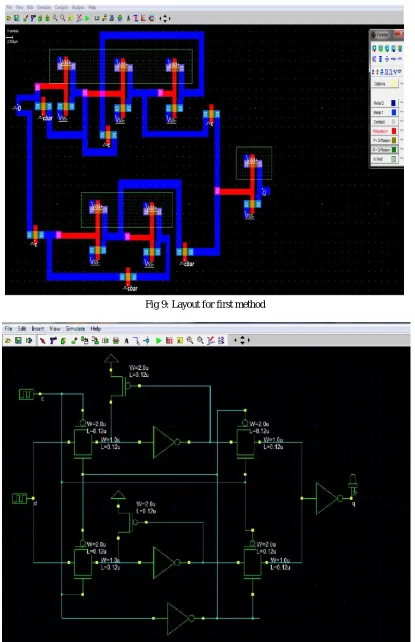
Fig 7: Schematic for first method
[image:6.612.110.496.461.706.2]
Fig 9: Layout for first method
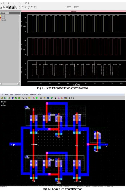
Fig 11: Simulation result for second method
[image:8.612.87.532.82.390.2]V. CONCLUSION
The designs based on pass transitor logic and on transmission logic gate. The new designs were compared to previous DET flip-flops using simulation in the 180nm CMOS technology. The DET FLIP-FLOPS design and derivatives were shown significantly to consume the area related to previous works which improves process speed but when concentrated on area some power consumption will be appear in the output and improve on Latch-MUX DET flip-flop designs in the area , which makes them useful for designs with large logic depth that are prone to glitching. The two designs which are more complex and competitive. Inp The novel CT_C and CTF_C designs can be used in high-performance scenarios as they were found to have superior power and power-delay products during periods of high switching activity. Extensive Monte Carlo simulations were carried out to demonstrate that the novel flip-flops are robust under process variations. The new FN_C design was found to be one of designs least susceptible to process variations. Voltage scaling simulations were performed that show that the performance of the presented flip-flops scales very similarly to DET flip-flops.
The DET flip-flops are simulated with different clock frequencies ranging from 1MHz to 10GHz. Simulation results show that the proposed DET flip flops based on pass transistors as well as transmission gate logic has reduced the area. In The simulation of 180 nm technology in HSPICE/MICROWIND
REFERENCES
[1] Stepan Lapshev and S. M. Rezaul Hasan, “New Low Glitch and Low Power DET Flip-Flops Using Multiple C-Elements”,IEEE Trans.Very Large Scale Integer.(VLSI) Syst, June 27’2016
[2] N. Nedovic and V. G. Oklobdzija, “Dual-edge triggered storage elements and clocking strategy for low-power systems,” IEEE Trans. Very Large Scale Integer. (VLSI) Syst., vol. 13, no. 5, pp. 577–590, May 2005.
[3] A. G. M. Strollo, E. Napoli, and C. Cimino, “Analysis of power dissipation in double edge-triggered flip-flops,” IEEE Trans. Very Large Scale Integr. (VLSI) Syst., vol. 8, no. 5, pp. 624–629, Oct. 2000.
[4] P. Zhao, J. McNeely, P. Golconda, M. A. Bayoumi, R. A. Barcenas, and W. Kuang, “Low-power clock branch sharing double-edge triggered flip- flop,” IEEE Trans. Very Large Scale Integr. (VLSI) Syst., vol. 15, no. 3, pp. 338–345, Mar. 2007.
[5] J. Tschanz, S. Narendra, C. Zhanping, S. Borkar, M. Sachdev, and V. De, “Comparative delay and energy of single edge-triggered and dual edgetriggered pulsed flip-flops for high-performance microprocessors,” Proc. Int. Symp. Low Power Electron. Des., 2001, pp. 147–152.
[6] D. E. Muller, “Theory of asynchronous circuits,” Internal Rep. no. 66, Digit. Comput. Lab., Univ. Illinois at Urbana-Champaign, 1955. [7] K. van Berkel, “Beware the isochronic fork,” Integr., VLSI J., vol. 13, pp. 103–128, Jun. 1992.
[8] S. V. Devarapalli, P. Zarkesh-Ha, and S. C. Suddarth, “A robust and low power dual data rate (DDR) flip-flop using C-elements,” in Proc. 11th Int. Symp. Quality Electron. Des. (ISQED), Mar. 22–24 2010, pp. 147–150.
[9] A. Gago, R. Escano, and J. A. Hidalgo, “Reduced implementation of D-type DET flip-flops,” IEEE J. Solid-State Circuits, vol. 28, no. 3, pp. 400–402, Mar. 1993.
[10] R. Hossain, L. D. Wronski, and A. Albicki, “Low power design using double edge triggered flip-flops,” IEEE Trans. Very Large Scale Integer. (VLSI) Syst., vol. 2, no. 2, pp. 261–265, Jun. 1994.
[11] A. Bonetti, A. Teman, and A. Burg, “An overlap-contention free true single-phase clock dual-edge-triggered flip-flop,” in Proc. IEEE Int. Symp. Circuits Syst. (ISCAS), May 24–27 2015, pp. 1850–1853.
[12] M. Alioto, E. Consoli, and G. Palumbo, “Analysis and comparison in the energy-delay-area domain of nanometer CMOS flip-flops: Part I—Methodology and design strategies,” IEEE Trans. Very Large Scale Integer. (VLSI) Syst., vol. 19, no. 5, pp. 725–736, May 2011.
[13] M. Alioto, E. Consoli, and G. Palumbo, “Analysis and comparison in the energy-delay-area domain of nanometer CMOS flip-flops: Part II—Results and figures of merit,” IEEE Trans. Very Large Scale Integer. (VLSI) Syst., vol. 19, no. 5, pp. 737–750, May 2011.
[14] V. Stojanovic and V. G. Oklobdzija, “Comparative analysis of master slave latches and flip-flops for high-performance and low-power systems,” IEEE J. Solid-State Circuits, vol. 34, no. 4, pp. 536–548, Apr. 1999.
[15] M. Alioto, E. Consoli, and G. Palumbo, “Analysis and comparison of variations in double edge triggered flip-flops,” in Proc. 5th Eur. Workshop CMOS Variability (VARI), Palma de Mallorca, Spain, 2014, pp. 1–6.