Oigi~al
Equipment Corporation
~Vlaynard,
Massachusetts
PDP-9
Maintenance Manual
OM09A
OM09A
ADAPTER/MUL TIPLEXER
MAINTENANCE MANUAL
1 st Pri nti ng October 1968
2 nd Pri nti ng October 1969
3rd Pri nti ng Apri I 1972
Copyright © 1968, 1969, 1972 by Digital Equipment Corporation
The material in this manual is for informa-tional purposes and is subject to change without notice.
The following are trademarks of Digital Equipment Corporation, Maynard, Massachusetts:
DEC FLIP CHIP DIGITAL
PDP FOCAL
CONTENTS
Page
1 • Introducti on 1
1 .1 Related Documentation
1
1 .2
Engineering Drawing References2
2.
Specifications2
2.1
Environmental2
2.2
Power Requirements2
2.3
Physical2
2.4
Controls and Indicators2
2.5
Performance2
3.
Installation3
4.
Principles of Operation3
4.1
Basic3
4.2
Detailed4
4.2.1
Power Turn-On4
4.2.2
Internal Control Pulse Train4
4.2.3
Single-Fast-Input Cycle5
4.2.4
Single-Slow-Output Cycle6
4.2.5
Double (Back to Back) - Fast-Output Cycles 75.
Acceptance Test Procedure 116.
Maintenance 116.1
General 116.2
Delay Adjustments 116.3
Module Complement 117. Engineering Drawings
12
ILLUSTRATIONS
1-1
Basic DM09A System Block Diagram3-1
Insta Ilati on Diagra m3
4-1
Control Pulse Train Circuitry5
1-1
4-1
4-2
4-3
6-1 7-1
CONTENTS (Cant)
TABLES Reference Documents
Single-Fast-Input Cycle Signal Flow Single-Slow-Output Cycle Signal Flow
Double (Back to Back)-Fast-Output Cycles Signal Flow Module Complement
Engineering Drawings
iv
8
9
10
12
1 • INTRODUCTION
The DM09A Adapter/Multiplexer an option to the PDP-9 manufactured by Digital Equipment
Corporation (DEC), provides an interface through which three I/O devices may gain access to the
PDP-9 memory via the DMA channel. A basic system block diagram is given in Figure 1-1.
Figure 1-1 Basic DM09A System Block Diagram
This document and the documents referenced herein provide the information necessary for
installation, operation and maintenance of the option. The leve I of discussion assumes that the user
is fami liar with the basic PDP-9.
1 .1 Related Documentation
The DEC documents listed in Table 1-1 contain material which supplements information in
this document.
Title
PDP-9 User Handbook
PDP-9 Maintenance Manual Volumes I and II
DIGITAL Logic Handbook
Table 1-1 Reference Documents
Document Number
F-95
F-97
C-105
Description
Operation and programming information for the PDP-9.
Operation and maintenance information for the PDP-9 including basic PDP-9 engineering drawings. Basic DM09A theory of operation.
[image:6.624.205.421.158.264.2] [image:6.624.61.569.444.706.2]1 .2 Engineering Drawing References
Engineering drawings wi II be referenced using an abbreviated code. As an example,
drawing D-BS-DM09-A-2, DMA Adapter Multiplexer Control, sheet 1 of 2, will be referenced as
[DM-2(2)] •
2. SPECIFICATIONS
2. 1 Environmental
The DM09A consists entirely of modules of the type used in the PDP-9 central processor.
Therefore, PDP-9 environmenta I specifications apply to the DM09A.
2.2 Power Requirements
The option obtains a II necessary operating power from the PDP-9 power supply system.
No additional power supplies, power control or fan assemblies are necessary.
2.3 Physical
The DM09A consists entirely of modules which are housed by two DEC standard 1943
mount-ing panels, thus requirmount-ing 10-1/2 in. of mountmount-ing space. Placement of these panels is given in
Sec-tion 3, IN ST ALLA TION •
2.4 Controls and Indicators
No controls or indicators are associated with the DM09A. The option is entirely under the
control of the PDP-9 and the I/O devices.
2.5 Performance
The multiplexer operates at two speeds. I/O devices with 10 mHz ·Iogic may request the
high speed and thus achieve a 1 .,.s/transfer rate; I/O devices with low speed logic should request the
low speed of 3 ~/transfer to permit sufficient data-line settling time. It should be remembered that
the speed range applies only to the DM09A. The PDP-9 DMA channel and the memory require only
1 .,.s/transfer.
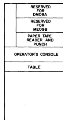
3. INSTALLATION
Implementation of the option involves insta II ing the option modules into their preassigned,
prewired locations in the basic PDP-9 cabinet. The location in which the option mounts is shown in
Figure 3-1 •
RESERVED FOR DM09A RESERVED
FOR ME09B PAPER TAPE READER AND
PUNCH
OPERATOR'S CONSOLE
TABLE
Figure 3-1 Insta Ilation Diagram
The following engineering drawings provide all necessary interface information.
Draw i ng Number
D-CD-DM09-A-9 (Rev. A)
CD-D-DM09-A-10
CD-D-DM09-A-11
Title
Memory Interface
Interface Cabling DM09 Memory
Cabling DMA Inter-Memory
4. PRINCIPLES OF OPERATION
4.1 Basic
Description
Interface between the DM09A and the basic PDP-9 memory.
Interface between the DM09A, ME09A memory extension control and MM09A extended memory bank.
Interface between the MC70B basic PDP-9 memory and MM09A, Band C extended memory banks.
A basic description of DM09A logic operation can be obtained from Section 3.8.3, DMA
Channel Transfers, of the PDP-9 Maintenance Manual, Volume 1. A detailed DM09A block diagram
is also contain in that section.
[image:8.618.260.363.157.354.2]4.2 Detailed
A variety of transfer type combinations are possible with the DM09A. To avoid excessive
repetition, only three types will be described herein; Single-Fast-Input cycle, Single-Slow-Output
cycle and Double (Back to Back)-Fast-Output cycles.
Certain DM09A operations are executed regardless of transfer type; namely, control circuitry
initialization via power turn-on and interna I DM09A control pulse train generation. Transfer type
descriptions assume I/O device 0 is being acted upon. All reference will be made to I/O device O.
Similar operations wi II result when any other device is acted upon.
All transfer types can be thought of as consisting of a number of "time states" each
commen-cing with a PDP-9 ClK pulse. Single transfers consist of time states in which either an I/O device is
made ready, in which a device is synchronized to the PDP-9, or in which a data transfer takes place.
With multiple transfers, synchronization is established during the previous data transfer.
When reading the logic descriptions, the user should refer to the engineering drawings
referenced on the signal flow tables. In addition, DM09A timing diagrams, drawings DM-8(1) and
DM-8(2) should be referenced for specific timing information.
4.2. 1 Power T urn- On
When the system is first turned on, PK ClR (power and key clear) pulses arrive at the DM09A
control logic and produce PWR ClR POS (power clear positive) pulses to condition the control logic.
The operations performed are as follows:
4.2.2
Clear SYNC 0
Clear SET AO
Clear SET DO
C lear DEY 0 CONT
Clear SLOW CYCLE A
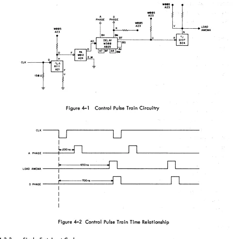
Interna I Contro I Pu Ise T ra i n
Following PK ClR, ClK (clock) pulses arrive at the DM09A control logic and are used to
generate an interna I DM09A control pulse train via the circuitry of Figure 4-1.
Time re lationships are illustrated in Figure 4-2. The pulse train is generated whenever the
system is ope rat i ng •
D
D H
ClK ---+---eI
t5en u
Figure 4-1 Control Pulse Train Circuitry
ClK
U
U
I
A PHASE
~oon.jl
n
I
n
n
~ 650n.
lOAD AMEMA
I
I
n
n
r
7OOn.D PHASE
Figure 4-2 Control Pulse Train Time Relationship
4.2.3
Single-Fast-Input CycleThe DM09A adapter/multiplexer is uti lized during the memory read/write cycle. During
this time the I/O device break request flag is set providing the DM09A with a CH 0 SK RQ level.
Referring to Table 4-1 and the referenced engineering drawings, internal control logic operations serve
to generate an AM RQ level. This level is applied to the PDP-9 memory control circuitry shown on
drawing D-SS-MC7Q-S-1 (sheet· 2). A ClK pulse marking the beginning of the SYNCING time state
is then produced. During SYNCING, the central processor has access to core memory. ClK, delayed
[image:10.612.86.566.69.560.2]SYNC(l) produces AM SYNC(1)B and AM SYNC BUS(l). AM SYNC(l)B is utilized by CM (control
memory) timing to prevent SM(1) from restarting the CM on the next ClK pulse which marks the begin-ning of the DATA XFER time state.
The DATAXFER time state is entered via another PDP-9 CLK pulse. ClK, delayed 50 ns,
is POST ClK and resets the MODE flip-flop conditioned by AM SYNC(l). MODE(O) signifies AM
access to memory while MODE(l) signifies CP access to memory. PRE-WRITE OFF of the previous core
memory cycle (SYNCING) sets the MEM DONE flip-flop and produces AM GRANT. If on EAE or an
lOT instruction immediately precedes the DM09A request, AM GRANT is not produced. In this case
AM SYNC(l)B is delayed to generate AM GRANT SMlTD (simulated).
During the current time state, I/O device 0 address bits are present at the input gating
circuitry of the AM REGISTER (refer to drawing DM-3(2». Address bits utilized by a PDP-9 with basic
memory are designated CH 0 ADDR BIT 05 through CH 0 ADDR BIT 17. The bits are applied to the
inverter modules shown. ADDR 0, the result of DEV 0 CONT(O) and SET 00(1), allows the address
bits access to the jam input gates of the AM REGISTER as LAM 05 through LAM 17.
An AMI (adapter multiplexer input) pulse jam transfers the 13-bit address into the register.
AMI is the result of AM GRANT* or AM GRAND SMlTD. The flip-flops designated AMEMA 03 and
AMEMA 04 are used with PDP-9 systems containing extended memory banks. Inverter inputs are CH 0
ADDR BIT 03 and SET AO(l) for AMEMA 03 and CH 0 ADDR BIT 04 and SET AO(l) for AMEMA 04.
lOAD AMEMA jam transfers the extended memory addressing bits into their respective flip-flops. This
pulse is produced 650 ns after CLK by the control pulse train circuitry described in Section 4.2.2.
Following memory addressing, an la-bit data word is jam transferred into the AM REGISTER.
I/O device 0 data word consists of CH 0 DATA BIT 00 through CH 0 DATA BIT 17. The data word is
also applied to a network of inverter modules. The enabling signal is DEV O. The data word is jam
transferred into the AM REGISTER by a second AMI pulse which is produced by AM STROBE.
4.2.4 Single-Slow-Out·put Cycle
Table 4-2 illustrates the signal flow associated with a Single-Slow-Output cycle. The
I/O device is programmed to indicate that an output transfer is to take place, the number of words to
be transferred and the address of the first word, DM09A control logic operations which result from this
type of data transfer are basically simi lar to those of the Single-Fast-Input cycle. The I/O device
requests multiplexer service via CH 0 BK RQ. The control logic proceeds to generate AM RQ and
AM RQ NEG. SYNC 0(1) and CH
0
FAST RQ condition the set DCD gate of the SLOW CYCLE A*Both may be present but the circuit is a logical OR.
flip-flop which is set by the positive going transition of AM RQ NEG. Following logic operations in
the multiplexer and in the PDP-9, an AM GRANT pulse is issued to produce AMI. With input transfers,
this pulse jam transfers the device supplied address into the AM register. This is not necessary with the
current type of transfer.
Following further DM09A control logic operations, simi lar to those of Single-Fast-Input
cycle, PDP-9 AM STROBE arrives at the DM09A. This pulse is gated with CH 0 RQ IN and SET 00(1)
to produce SAl (sense amplifier input) thus allowing PDP-9 sense amplifier bits SA 00 through SA 17
access to the jam input gates of the AM register. A second AMI pulse is produced at this time to jam
transfer these bits into the AM register.
4.2.5
Double (Back to Back)-Fast-Output CyclesSigna I flow for the current transfer type is given in Tab Ie 4-3. Initia I signa Is sent to the
DM09A control logic are CH 0 BK RQ, CH 0 FAST RQ and CH 0 RQ IN. CH 0 BK RQ signals the
DM09A that service is requested. This signal and internal SLOW CYCLE A(O) produce SYNC 0 EN to
condition the set DCD gate of the SYNC 0 flip-flop. The 0 PHASE pulse preceding the SYNCING 1
time state sets SYNC 0 to establish device priority. This conditions the CH 0 FAST CLR and sets the
DCD gate to produce AM RQ and AM RQ NEG. AM RQ signals the PDP-9 that a DMA cycle is
de-sired; the computer responds with AM SYNC(l) B.
The A PHASE pulse of SYNCING 1 sets SET AO and generates CLR SYNC. This clears
SYNC O. SET AO(l) and AM SYNC(l)B generate SET DO EN which conditions the set DCD gate of the
SET DO fl ip-flop.
The following D PHASE pulse sets SET DO. SET AO(l) and SET DO(l) produce CLR SLW CYC
EN which with A PHASE, maintains SLOW CYCLE A (0) , a characteristic of fast transfers. SYNC 0 is
set again because SLOW CYCLE A(O) and CH 0 BK RQ are sti II present. Setting SYNC 0 generates
another AM RQ signal. Because this signal is applied to the PDP-9 AM SYNC flip-flop prior to SYNC
CLK, the flip-flop remains set.
The PDP-9 produced AM GRANT arrives at the multiplexer control circuitry as the DATA
XFER 1 and SYNCING 2 time states are entered. The pulse jam-transfers address information into
the AM REGISTER. During these time states the data transfer associated with the preceding syncing
operations, and syncing operations for the next data transfer take place.
AM STROBE arrives from the PDP-9 and generates SAl and AMI, thus allowing the sense
amplifier bits, SA 00 through SA 17, access through the AM register gating circuitry and into the
AM reg ister •
DATA XFER 2 is entered. SET AO is cleared and operations similar to DATA XFER 1 take
place to jam transfer the data bits of the second word into the AM register. The 0 PHASE pulse at
Time Control
State Pulse
D PHASE
SYNCING A PHASE
D PHASE
DATA XFER A PHASE
D PHASe
Table 4-1
Single-Fast-Input Cycle Signal Flow
Signal Conditions
SYNC 0 EN CH 0 BK RQ
*
SLOW CYCLE A(O)SYNC 0(1) D PHASE
*
SYNC 0 ENAMRQ SYNC 0(1)
AM SYNC(l)B From PDP-9
SET AO(l) A PHASE
*
SYNC 0(1)CLR SYNC A PHASE
*
AM SYNC(l)B(B)SET DO EN AM SYNC(l)B
*
SET AO (1)CH 0 FAST CLR CLR SYNC
*
SYNC 0 (1)SYNC 0(0) SYNC 0(1)
*
CLR SYNCSET DO(l) D PHASE
*
SeT DO ENCLR SLW CYC EN SET AO(O)
*
SET DO(l)AM GRANT From PDP-9
CH OADDRACC A PHASE
*
SET AO(l)*
SeT DO(l)IN
DEY 0 CONT(l) CH 0 ADDR ACC IN
*
SET DO(l)DEVICE 0 DEV 0 CONT(l)
*
seT DO(l)*
CH 0 RQ INSET AO (0) A PHASE
*
SYNC 0(0)*
SET DO(l)CH
o
ADDRACC CH 0 ADDR ACC INSLOW CYCLE A(O) A PHASE
*
CLR SLW CYC ENAM STROBE From PDP-9
CH 0 DATA RDY D PHASE
*
SET DO(l)*
SLOW CYCLE D(O)IN
INH 0 DAP(O) CH 0 DATA RDY IN
CH 0 DATA RDY CH 0 DATA RDY IN
CH 0 DATAACC D PHASE *CH ORQ IN
*
INH 0 DAP(O)~ S~T qO{l)seT 00(0) D PHASE
*
SET AO(O)*
SLOW CYCLE 0(0)Drawing Number
DM-2(2) DM-2(l) DM-2(2) MC-l(2) DM-2(1) DM-2(2) DM-2(2) DM-2(1) DM-2(1) DM-2(1) DM-2(1) MC-l(2) DM-2(1)
DM-2(1) DM-2(2) DM-2(1) DM-2(1) DM-2(1) MC-2 DM-2(2)
[image:13.793.61.698.111.499.2]Time Control
State Pulse
SYNC D PHASE
SYNCING A PHASE
D PHASE
DATA XFER A PHASE
D PHASE
Table 4-2
Single-Slow-Output Cycle Signal Flow
Signal Conditions
SYNC 0 EN CH 0 BK RQ
*
SLOW CYCLE A(O)SYNC 0(1) D PHASE
*
SYNC 0 ENAMRQ SYNC 0(1)
SLOW CYCLE A(l) SYNC 0(1)
*
CH 0 FAST RQ*
AM RQ NEG ... 0AM SYNC(l)B From PDP-9
SET AO(l) A PHASE
*
SYNC 0(1)CLR SYNC A PHASE
*
AM SYNC(l)B(B)SET DO EN AM SYNC(l)B
*
SET AO(l)CH 0 FAST CLR CLR SYNC
*
SYNC 0 (1)SYNC 0(0) CLR SYNC
*
SYNC 0(1)SET DO (1) D PHASE
*
SET DO ENAM GRANT From PDP-9
CH 0 ADDR ACC A PHASE
*
SET AO(1)*
SET 00(1)IN
DEY 0 CONT(1) CH 0 ADDR ACC IN
*
SET DO(1)SET AO(O) A PHASE
*
SYNC 0(0)*
SET DO(l)CH 0 ADDR ACC CH 0 ADDR ACC IN
CLR SLW CYC EN SET AO(O)
*
SET D(1)SLOW CYCLE A(O) A PHASE
*
CLR SLW CYC ENAM STROBE From PDP-9
AMI AM STROBE + AM GRANT
SAl AM STROBE
*
CH 0 RQ IN*
SET DO(l)SET DO(O) D PHASE
*
SET AO(O)*
SLOW CYCLE D(O)Drawing Number
DM-2(2) DM-2(1) DM-2(2) DM-2(1) MC-l(2) DM-2(l) DM-2(2) DM-2(2) DM-2(1) DM-2(1) DM-2(l) MC-l(2)
DM-2(1) DM-2(l) DM-2(1) DM-2(1) DM-2(1) ' DM-2(1)
MC-2 DM-2(2) DM-2(2)
[image:14.799.80.713.109.487.2]...
oTime State
SYNCING 1
DATA XFER 1 SYNCING 2
DATA XFER 2
Control Pulse
o
PHASEA PHASE
o
PHASEA PHASE
o
PHASEA PHASE
[image:15.797.98.691.115.560.2]o
PHASETable 4-3
Double (Back to Back)-Fast-Output Cycles Signal Flow
Signal Conditions Drawing
Number
SYNC 0 EN CH 0 BK RQ
*
SLOW CYCLE A(O) OM-2(2)SYNC 0(1)
o
PHASE*
SYNC 0 EN OM-2(1)AM RQ SYNC 0(1) OM-2(2)
AM SYNC(l)B From POP-9 MC-1(2)
CLR SYNC A PHASE
*
AM SYNC(l)B(B) OM-2(2)CH 0 FAST CLR CLR SYNC
*
SYNC 0(1) OM-2(l)SET AO(1) A PHASE
*
SYNC 0(1) OM-2(1)SET DO EN SET AO(l)
*
AM SYNC(l)B OM-2(2)SYNC 0(0) CLR SYNC
*
SYNC 0(1) . ,DM-2(l)
SET 00(1)
o
PHASE*
SET DO EN OM-2(l)SYNC 0(1)
o
PHASE*
SYNC 0 EN OM-2(1)AMRQ SYNC 0(1) OM-2(2)
AM GRANT From POP-9 MC-2(1)
CH 0 AODR ACC A PHASE
*
SET AO(l)*
SET 00(1)IN DM-2(l)
CH 0 ADDR ACC CH 0 ADDR ACC IN DM02(l)
OEV 0 CaNT (1) SET 00(1)
*
CH 0 ADDR ACC IN DM-2(l)AM STROBE From PDP-9 MC-2
SAl CH 0 RQ IN
*
SET 00(1)*
AM STROBE DM-2(2)SYNC 0(0) CLR SYNC
*
SYNC 0(1) DM-2(1)CH 0 FAST CLR CLR SYNC
*
SYNC 0(1) OM02(1)CH 0 DATA ROY
o
PHASE*
SET 00(1)*
SLOW CYCLE 0(0) DM-2(2) INCH 0 DATA ROY CH 0 DATA ROY IN DM-2(2)
AM GRANT From PDP-9 MC-2(1)
CLR SLW CYC EN SET AO(O)
*
SET OO( 1 ) DM-2(1)SLOW CYC LE A (0) A PHASE
*
CLR SLW CYC EN MC-2(1)CH 0 AOOR ACC A PHASE
*
SET AO(l)*
SET 00(1) OM-2(1)IN OM-2(1)
CH 0 AODR ACC CH 0 AOOR ACC IN
AM STROBE From POP-9 MC-2
SAl CH 0 RQ IN
*
SET 00(1)*
AM STROB'E OM-2(2)5. ACCEPTANCE TEST PROCEDURE
Acceptance testing of the DM09A option consists of executing Test Procedure DM09A-O
with the DM09A Tester at both normal operating conditions and the voltage margins specified below.
Trial Test Aggravation
Condition
1 DM09A-O None
2 DM09A-O Margin rack A
3 DM09A-O Margin rack B
Minimum margin specifications for rack A and rack B are listed below.
Margin
+10V -15V
+6V
I
-6V +4V 1-4V6. MAINTE NANCE
6.1 General
The general maintenance procedures described in the PDP-9 mainteoonce manual also
apply to the DM09A option.
6.2 Delay Adjustments
Adjust the R302 Delay at A27 according to the data given on engineering drawing DM-2(2).
603 Module Complement
[image:16.621.218.414.134.230.2]Table 6-1 Module Complement
DEC Type Module Type Quantity Recommended Spare Quantity
8169 Inverter 17 2*
8213 Jam Flip-Flop 14 1*
R002 Diode Cluster 2 1*
R111 Diode Gate 12 1*
S107 Inverter 2 1*
S202 Dual Flip-Flop 7 1*
S203 Triple Flip-Flop 1 1*
5603 Pulse Amplifier 5
Woo5 Clamped Loads 3 1*
W300 Delay Line 1 1
W612 Pulse Amplifier 8
R302 One-Shot Delay 1 1*
*Contained in the basic processor spare parts kit.
7. ENGINEERING DRAWINGS
Table 7-1 lists the DEC engineering drawings associated with the DM09A option.
Drawing Number
DM-2(1)
DM-2(2)
DM-3(1)
DM-3(2)
DM-4(1)
DM-4(2)
DM-5
DM-8(1)
DM-8(2)
Table 7-1 Engineering Drawings
Title
DMA Adapter Multiplexer Control BS-DM09-A-2
DMA Adapter Multiplexer Control BS-DM09-A-2
AM Register BS- DM09-A-3 Sheet 1 of 2
AM Register BS-DM09-A-3 Sheet 2 of 2
Cable Diagram BS-DM09-A-4 Sheet 1 of 2
Cab Ie Diagram BS- DM09-A-4 Sheet 2 of 2
Module Uti lization MU-DM09-A-5
Sheet 1 of 2
Sheet 2 of 2
DM09A Timing Diagram TD-DM09-A-8 Sheet 1 of 2
DM09A Timing Diagram TD-DM09-A-8 Sheet 2 of 2
12
Revision
J
J
B
B
0
A
[image:17.620.63.564.81.705.2] [image:17.620.67.558.414.679.2]D
c
B
A
8 7
CH 0 ADDR Ace ~N
CH ¢ AClOR ACC
SET D 10). L
A PH,AS£ K 6
CH I AOOR ACC XN
011 Rq IN
Wal05
el9
5
CH I ADOR ACC
SeT A2(1)
SET 02(1)
.4
CH 2 "'OOR Ac.e IN
ACC
C.H Z RQ IJi'---.-:v----'-"'I vrfJr,Js
CI9
SLOW CYCLE 0(1)
3
CH 2. AODR ACC
C H 0 RQIJN-~-=-t~ N' 1\ I we(i1S
CI9
CH 2. DATI>. ACe
2
CH (/J O"TA ACC
SLOW'· CYCLE 0(1) :It
.AI PIfASF --t>I5~-«52'1
PWR' CLf{ POS-~::r'""-...:..O.,...
11 PHIISE
flMRQ-'IEG.
SLOW CYCLE 0(1)
c
A PHASE CLR CH '2. F ... ST C.LR
o;:;,ET 0 (6(1)
PWR CLR PO~ ~~UL~~-L----~~~~~~----~~fU~~~----~~~~~~---~~~~~~~ ______ ~~~~~~
D PHASE
CL R '5YN C .:::..{;tg;J----+---....:.N~Zl---_+_---'::O"018J
:SET 0 Z.(I")
SYNC 1])(1) :SYNC. 1(1) :SYNC eel) CH ¢ DATA ROY Ij,j CH I DATA RD,{ IN CH 2 Oo'o.TA RDY IN
CH If> AOOR. ACe. IN CH I "OOR Ace. IN CH Z ADDR ACC IN
8 7 6 5
SETIl~(I) SET D '1(1)
CH 2.
B
~---_+---_+--OCLR SL VI' eye EN
3
A
2
8 7
D
CH ¢ 6K RQ
CH ~ DATil RDY IN
c
•
B
CHa1RQTI'l H
A
8 7
6
SET D 2 E.N
~---'--':'-=-.IrN7\l--.AM SYNC(I)S(e.)
SYNC. e \;:N
RDY
K
L
p
SYNC Z (¢)
A f>HjI,.SE
snlC 2. (91)
6
SYNC ¢ (I)
SYNC. I (I)
SYNC e(l) D 5
P
5 K
F
F
AMI
H
SAl.
A
'" PHASE (6)
AM RQ. NEG.
D
3
CH ~ RQIN U
DEV 'Ii CONTROL(t)
SE.T D¢(I)
DEV 1 CONTROL(I)
SET o I (I)
WI!J¢5
1'.2.3
CH I RQ IN
I.. 011 D
.IIMEMII
CH a RQ IN
DEV a CONTROL(I;
SE.T D 2.(1) U
PK CLR
ISqI./I..
3
K
U
1\
V
v
PWR ("LA. p05
2
DEVICE ~
DEVI(.\;' \
.11M G.RIjNT SMLTD
I'lM SYNC(I)B---£~~
2
I1DJUST AM GR/Jf(T SMLTO
TO occuR AT AM GRIII"r TIME.
D
c
B
A
BS-DM09-A-2 Sheet 2 of 2 DMA Adapter
Multiplexer Control
o
c
8
A.
8
SAO" SAl
01 a DATA-BIT()0'
DEY fI
CH I ~TA-BIT0'0'
DEVI CH 2DATA-BlT~
NOTE:
7
C
loon,
tw,
10". TERM I NATORS TO GROUND MUST BE PUT ON SA!Il0 THRU SA 17.8
SA 12 SAl
01 0 DATA-BIT 12 DEv0 CH I {)I.TA-BIT 12
DEVI CH 2 DATA-BIT 12
7
6
M C
=- -=- -=
N P N
M
6
5 3 2
D'
c
C C C
-=- -= -=- =-
-=-loon
8
C hi C
-=-
-=-A.
5 3 2
D
8
i-C~J AYE",A
CH (\ ADOF\
81T03-SET A0111
CH I ADDR BIT 03 SET AI II)
CH 2 ADDP. 81T03
SET A2 III
E
M
0 E 0
CH I AODR S
BIT 04
CH 2ADOR
BIT 04
7
P N P
fM
DDI\ C
-=- ':'
6 5
LAM £15
CH0ADDR IIj CH 0AODR CH '" ADDP
BIT 05 BIT 06 BIHJ7
CHIADDR S CHIADDR CHIADDR
BIT 05 BIT 06 BIT 1217
CH2AOOR V CH 2 ADDR CH 2 AODR
BIT 05 BIT 06 BIT 07
M M
-= -=- -=
.4 3 2
D
LAM (67 LAM 08 LAM~9 LAM II LAM 12 LAM 13
IIj CH0ADDR CHI2lADDR CH 0ADDR CHi2IADDP
BIT 08 BIT 09 BIT IfIJ BIT II
CHIADDR
BIT 08
CHIAOOR S CH I ADDR CH I ",uDR S
BIT 09 BIT II BI T 12 81 T 13
CH 2 ADDR V CH 2ADDR C H 2 ADD ~ V C H 2 A DOR V
81T 1iJ8 BIT 09 BIT 10 BIT II 81 T 12 BIT 13
C M C M C M C
-= -=
c
CB
A
:H0ADDR BI T
ADDR iJ
CH I J.OORBIT 14
ADDR I
CH2 ADDRBIT 14
ADDR 2
8
LAM 14
M
(H0 ADDR BI T ,5
C'" IAODR S
BIT 15
CH2 ADDR V
BIT 15
LAM 1'5
C
7
LAM 16
M
CH2ADDR V
BI T 17
6
W!1l05
'A23 H
LAMI7
ADDR fJ ADDR I ADDR 2
DEV
L
C SET 0 0( I )-,--T.-."" - " SET 0 2 (I) ,H-,-~--,.,---,K
B
A
5 3 2
BS-DM09-A-3 Sheet 2 of 2 AM Register
8 7
o
c
B
A
8 7
CH ¢ BK RO
I
RO INj
~~~: :~~
DATA ROY FAST ROCH 0 FAST CLR
CH I BK RO
RO IN
DATA
FAST RO
CH I FAST
CH 2 BK RO
RO IN
ADOR ACC
DATA ACC
FAST RO
CH 2 FAST CLR
6 W¢31 D08 Wf/J31 DI2 6 CLK
AM SYNC(I)8
AM RO
AM GRANT
PK CLR
5 4
G795 W(/J33
AIS
*
A(/JISA 1/J0 SA 09
II W(il33
A02
AMEMA 03(01--.1.,----1 ..
f/JI 02 03 04 1/J5 06 (/;7 12 13 14 15 16 AM STROBE
AMEMA 04 (0} ... " __ +-_t-eV SA 08 SA 17
*
USED FOR TERMINATION ONLY NOT A CABLE.(OPTIONAL)CH rtJ 8K RQ CH 0 RO IN
CH ¢ FAST RO
CH I BK RQ
CH I RO IN
CH I FAST RO
CH 2 BK RO
CH 2 FlO IN
CH 2 FAST RQ
AM 09 (I) Ic;l 12 13 14 15 16
AM 17 (Il W031
013
*"
5
AM f/J0 (I)
01 1/J2 03 04 05 f/J6 07
AM 08 (IJ
AM ¢9 (Il
I~ II 12 13 14 15 16
AM 17 IJ)
W!2l31 A03
AM (/J(/J (I) 01 02 03 !/J4 05 06 07
AM (jI8 (I)
W¢31 W031 DI/J2 006
rJj' (0'
E E
H H
K K
M M
- P P
~S
S
--"T T
--..
~V V
'-" '-"
WI/l31 010 (!5' E H K M P S T
Iv t
t::Hc;J) (CH I) (CH 2)
(CH r)
W¢31
0~J7
(CH 2)
W031
DII
4
NOTE:
PINS C,F, J,L,N,R,U
ARE GNO FOR ALL
w031's AND WI/J33'S
3 2
o
c
B
A
3 2
D
c
B
A
8
c'"' \" C'f-Tf-
,
a,TI
7
iW~¢Io-·' W031
I ClIO : CQlI
I I
¢¢ I DI ~
cf> I - - , - - -... , . ~
q)'2 .... --:----~ ~
K
cb~ ...;---....:...;...~
M
¢a,- -;---=~
P
¢5 ~--"----;-<"
¢/& ~
T
¢.-, ---:-I---~·
I V
CH (/J DI>.TA BIT ¢B -71--...,,....
L _ _ _ ...l
W~31
c.¢'7 D
CH I ,t..ODR EIT ¢~
cpa,
8
5
--;--.... r...
,
7 II 12-I~ I'::> 1<0
CI4 0 DA,"" S\, 11
CI-! I I>.DDR B I t ¢9
I(j, II 1'2. 13 1<+ IS \10
CH \ "'DD~ '0\\ n
6 T --;--.,:.:-.1 • V ---'-I--~I"· 1wcbct>=-
~
L~~ __ J
L: 0
--,----1,....
MI E
--;--~;...IItI.
NI H
---:----I~·
F'I K
--;--"R~IItI:-, ~: p
---:----,....
.. ,-I -;:,---:----:...,I~·
\}I T
-!..--~~.
'I! V
--'----,...
___ J.
6
07
CI-I(/) "-OOR SrT ¢s
CI4 2. DATA. SI\" ¢¢
q,\ ¢'2.. O~ ¢4 d>s ¢xe. <$'1
CHZ Dt>..\"A. BIT ¢-e,
5
W{!I31
CIjZI~
I)
rw¢¢i5il W¢31
: CI<O I c.¢"?J I
I DI o
-,,-I '6.
-";'--~I'-44 •
1""1 1-1
,_1'44
-1-11 K
-..;.----I~ •
J, M
- " ; ' - - FI
:-4oI-\'(1 p
Li '5
...:._--,....
~ T
--,---+-'-"" •
-..;. _ _ .. N...;.;I'-44 ~
L ___ J
·OPTIONAL CLAMPED LOADS.
5
4
CH ¢ r-.1)t:>R SI\" QJ9
I ell
\I
1'2..
\~
\<0
CH (/> M)DR. SIT \"7
CH2. D"""''''' BIT o;zl'?J
\q, II \'2. \3 \'4 4 o
Ml E
-'--+--''"""'1 eI • NI I-!
- - : - - + - ' -.... 1 eI • PI \<,
--;--~I~·
RI M
- - - . - - -.... 1 . . •
~I 'P
,:
~ --;--~I,.IJI \
--;----I~· \/1 V -+---~.
rvj~¢5"""il
I CIS I W031 I I CI~
I pi 0
.
Rl E...:.--~-41.
5:
1-1--i----~.
T: K
- ; . - -
....
,.-ul M --;----1-41
v I F'
-;:r.::-:-=--=-~-:::l· •
I LI ~
: Ml T
I NI V
--i-I---I~ •
iWci>¢5 :
LC~:""'_J
3
CH I Di'.T~ 51\
t
<:bch I/J\ (M .... ¢~ ¢a,-¢'O ¢ro ¢"1CI-l \ 01>.,,,", ' 0 \ \ ~'e,
CH '2. ""DDR.
1
CH 2. t--DDR B\\" ¢~
3
EI E
-;---~I" •
FI \-\
-'----.
....
K
·
-'----
....
p...,...---.
....
-;:. ...,...--_-41--:----.
....
V --;----.....
W(ll31 ell D -E·
1-\ K•
·M-;---~I·-101 P
-;---"I~
1-\1 '5
-;----
~I...
-T
...,...--_.-
V--;----,....
CH 1 D"-,,,, an' t:p9
\(j) \1 IZ. \~ \4 \S
CH Z. ADDR. BIT ¢~
Iq, 1\ 12-\~ Iq. IS \(0
CH Z. I>..t>OR e l l \ I
2
2
rw~¢~-;tl (It..:
lC{N : ':;."/;'<>
I~/lr-pl "::
I--'A-?: ~!
-:---~.'
1-1
-;----~.
"'-~--~I"· -;-~:-:-.. J~I~ •
K:
I---'-1----4~i~
iwa'>c:t>:. I
LC~':_J
fW"0-~5~
I CI'::. I W<!S31 I I
<:"IZ-LI D
•
M! EOI
.
H
PI K
-;----,....
R: M
si
p---:---FI~·
~
__ .. T-,-,I,.;
ul T
...;.--..
v-:,...~--.---,,....
L _ _ _~
D
c
B
A
BS-DM09-A-4 Sheet 2 of 2 Cable Diagram
8 7 6 5 3 2
2 3 4 5 6 7 8 9 10 II 12 13 14 15 16 17 18 19 20 21 22 23 24 25 26 27 28 29 30 31 32 33 34 35 36 37 38 39 40 41 42 43 44
11833 1833 U33 W~33 'lYJL33 ~213 Jl1ll Jl213 8213 8213 8213 B213 B213 &213 s~n" 1.12 HII: Kill _~'7 ~2~ _1!J11 ~5 !i12 -.!W. ~ 1::>61Z'~
D
m
~ AMG~~T
'"
/
A2111 A23F AZ8i GRNT
ClM 2QL
F- - I BZ8T S SMlT[ ISMlT
~
V
All All All All All All AM All All - rsYMC
fMi~ All B19J AlII A1811
:A PHAS Al50 III .2
,,.
"
18 ,1.8 12 14 16 r - -- - - ' - ' -SYNC RQ P'
-~
V
CONT. ONTROL r - - (I)
I!:'~
SA SA AM All FRO!,! FROM
""' 18S _ iPHASi
_'2IfI_
AA
MEM. E/IORY - AIIH - SPARE r---- r
-~
V
8-2 9-17 (,21-8 9-17 LEVEL (B) r - - - I'tlASE
TERM. r
-l¥l-
r - - ~AM All AM AM All AM All AM All r - - 2 - r---- I
~
V
I
SJI r - - E
,81 .3 '5 '7 as 11 13 15 17
r-A1BR~ AleF r
-f - - ~~~)1.
r - - 1
824P
~
L
B19L A17L
ISNN
B169 8169 ~169 --"-169 8189 8169 8189 9169 9169 9169 9169 9169 B189 9189 B 69 8119 9189 R I 8213 8213 8213 l18li2 8zl~ 1::>110 ( ~ S7JI': R . /
11.
D
Clf\
/
""
919Y SlW
iAMEMA
~AlIK
r - -~MEMA
~
r- - CYCV
~
LAM LAM LAM LAII LAM LAM LAM LAII LAII LAII LAII LAII LAM LAM LAM ADDR lDOR DEVICE SLOW OEV ,!
913 EN
(63 8S 18 18 II III 12 12 14 14 16 18
,
2 1 B7JI't H!'- CYCLE CONTROlV
118 112 ,84 liS r
-~
r - - r-'"
r---- A ClR
AllL
RQif;
0 SLW
B28v r--- r----r 92. t
-V
'"
fi!o
PHASE CYCI
r---- EN
r - - B21L fllMEMA j'lMEMA SLOWr- -
r----V
'"
LAII LAII IAMEMAj LAII LAII LAII LAM LAII LAII LAM LAII LAII LAII LAM LAM LAM LAM ADOR DEVICE ~EYICE IG~'4 YCLE DEY I Clf\
I--~i7ii_ r - - 04 0 - CONTROl SLW
111
13
J
~4J
85 85 17 .07 ,89 19 11 11 1.3 13 15 15 17 17 1 I 2 ~t-V
'"
B21V CYC
EN B
c
c
2 3 4 5 6 7 8 9 10 II 12 13 14 15 16 17 18 19 20 21 22 23 24 25 26 27 28 29 30 31 32 33 34 35 36 37 38 39 40 41 42 43 44
W0.31 W031 W~31 'K~31 jWl2l3 'K0M U't£l~J W~ 31 IW031 W031 W031 IW0.31 l1li5" l1li5 • 1 _ - l1li5" _ 5 " l1li5" _5 1_5 15603 ~ll -Rll --.S2.I.L l..S2I.2. -.S2U ~?.II? ~?.II7 R I D
'"
LB
c
~ .C23f
'"
V
can C23L
Ol8F
--"'I2.l ~ ~YNC t-~TD rJ<25E_ C2BP
'"
V
ClIBS C2.311 I EN , EN SET SET SET SYNC SYNC
~ r- CHB CH I CH 2
f----casT C23N o ,8 o 2 A 1
,
2I
DATA I
CBSV C2.3U
~
V
CH '. CH 1 CH 2 CH, CH 1 CH 2
Cl'S SYNC B
C25P C27E _
C1.IT ISYNC E DleR ~V~'ir I-SET 0
DATA DA.TA ADDR ADDR DATA ADDR AD DR DATA DATA ADDR ADDn AODR AOOR AODR DATA DnA DATA SPARE 1 (,n
~
V
BI T BIT BI T BI T BIT BI T BI T BIT BIT BIT BIT BIT BITS BITS BITS BITS BITS BITS LI.'
8-8 9-17 3-8 9-17 11-8 9-17 3-8 9-17 '-8 9-11 3-8 9-17 83-11 83-11 83-11 18-14 ,88-14 ,88-14 B27D
92711 SEl SET SET SYNC DEY 2
'"
V
B27R
fJ261..
0240 SYNC ~E~D_ o I A, A 2. 1 ONTROl C27P
DI~F r-2 Ell
~
/
024H 024L
W~31 W£l31 1831 W031 WIZ'31 1831 We:J31 W031 1831 G7115 W612 W612 '612 WU2 1112 1612 RIll S6.0i Rill S-6.1II" Rill S6!iJ~ S203 . / ,
CH $I CH 0' CH¢ INH
V
'"
ADDR AOOP. OISR_ DATA t-D~~B.. 019P. 0
/
~'"
CH ," CH 2 CH 1 CH. CH 2 CH 1 ACC ACC f\OY DAP
4 - - CH I CH 1 CH 2
--
ADDR AODR AODR FUT DAn DATA ININ
ACC ACC ROY CLR CLR ACC IN
V
CH 1 CH I CH I INH
eH AOOR AODP. DI1F _ DATA t-Df~
L D2rdF J.
V
I"'~
AM All CONTRO AM All CONTRO All AM ONTIIOL' ',1,2 ACC
ACC f\DY OAP
SPARE 1-8 9-17 SIGNAL SPARE ,8-8 9-17 SIGNAL SPARE lI-a 9-'17 IGNALS LEYEl SPARE I IN
(NEG) (NEG) (NEG) (NEG) (NEG) (NEG) TERM IN IN
I CH I
eH '. CH 2 CH I CH·ICH2
V
~
AOOR DATA DATA FAST DATA DATA CH 2 CH 2 CH 2 INH
ACC RDY RDY CLR ACC I ACC ADDR ADDP. DI71!... DATA t-°f~ &. D20P. 2
ACC
ACe. P.DY OAP
V
~
IN
IN IN
D
B
• OPTIONAL MOOUlES. NOTE: FOR IIODULE COIIIT SEE A-PL-DI&89-A-5
A A
8 7 6 5 4 3 2
8
D
c
B
A
8
7 6 5 .4 3 2
COMPUTER BASIC. C.YC.LE
A PHASE PULSES (i20 NS)
(INTERNAL DM09A)
D PJ-1ASE PULSES (I20NS) (INTERNAL DM0911)
C.HX 81'1 R~
(F"ROM DEV X TO DIVl09A)
SYNC X
(INTERNAL DN/0911)
AM RGI
(rRO,'vl Dl'r') 0 9fi TO ""Etr'ORY)
AM SYNC (i) B
(FROM M£MORYTO DM0911)
SErf! x
(If'lTERNfiL DM0911)
CH X FIIST Rq
(FROM DM091l TO DE.V x)
CHXRQIN (FROM DEV X TO DM0911)
SET D X
(iNTERNAL D/'IJO 9/1)
SLOW CYCLE
(INTERNAL DM0911)
~
SINGLE'FA5T'INPUT
CYCLEf1
SYN INI
SINGLE. SLOW, OUTPUT CYCLE:0
SYNCiNG
au
FAST CLEAR:, ADDR ACCEPTED X ~
\
\
~~J---~~-_-_~-L__
~__
-3 ___ ~-L~_~-~-'---~~-_-_-'~ ________~/~~/~---~
~OW CYCLE (D). 01)( SK RQ (-3)'D PHASE- - - -
U
AM 5 ,(NC (I) B·1l PHASE
SYNCX-I~,---
_ _ S_Y_N_C._X ___ O ___________________~r::''---
________________________________________
~,~---: I 200NS--: ~ I :
200 N MAX S
~
:r---\
f--- MAX ':.
!!---.'---____________________________
L 4_0_0_N_S MAX __ ---.----'-'---' ... /r' - - - , 1 . . -______________________ _CC
YNC X (I)-A PHASE'----J
SYNC x(o)· SET D X (I). i9 PHIlSE
'--_ _
---'I
5£TM.A.""("B.~
SLOW CYCL£:(O)-SETAX(O)'D
r
CHX FAST RQ (-3)'SYNC.X(I}·Il'M RG/---3PHASE .
---~ to 9 /'liS /lI
7 6 5 .4 3 2
TD-DM09-A-8 Sheet 1 of 2 DM09A
Timing Diagram
27
D
c
B
8 7 6 5 4 3 2
D D
c
B
A
8
Ai';, GRANT (F i' (;M ME/IIOR f TO DWi0911)
AM STROBE
(FROM MEMORY TO DM091i)
ADDR ACC£. PTED (Ui X)
(FROM DM09-"l TO DEV X)
Dt'iTA READy (U/X)
(FROM DM09A TO DEY X)
CA-:-A ACCEPTED (CHX) .
(FROM DIVI() '7/1 TO DEli X) C H X IlDOR (FROM DEY X TO D/Vi091l)
CH X DATA
(FROM D£V' X TO DM09!1)
5ET'lS£. /l MPS
((",,<a.VI MEi/lORY TO D1YI0911)
AM LOADED
(F ROM DfYl09fl TO DH X ¢
MEMORY)
C H X FIlST CLEItR
(FROM DIYl091i TO D£V)()
7
U
(120 NS)~SET D X (I)' SET II x{I)· A PHIISE
- - - t U (320 NS)
u
_ _ _ _ _ _ _ _ _ _ _ ----I~ SLOW C yeL£. (!IS) 'SET D X (I). D PHASE.
U(320 N5)
_ _ _ _ _ _ _ _ _ _ _ ----I~CHX RQ IN (-3)' SET D )«(1)'D PHASE
Uf320 N5)
u
u
u
ADPR ACC.EPTED X="
\ ---.l / ~'
Y
~/~~~~~---~--~ DATI'! ACCEPTE.D X ' - - - " - - - ~ I I I~----~---~ ~ ~
U(320 NS)
GRANT
AM STROBE
u
'~-D-A-T-~-~-~-~I-D---~~~;'~~DA~T~A~V.~A~L~ID---y
~SYNC x-¢
---1U (32 0 NSj
6
u
5 4 3 2
TD-DM09-A-8 Sheet 2 of 2 DM09A
Timing Diagram
c
B
)
p
lot
r---~~---~~---4~---~---OGND
R4
100,000 R8 100,000 RI2 100,000
A
t_---~~+_---O +IOV CI
.01
.... 0
B
~---+_----~---+_----~---+_----~---~---~~_e---G-15V
R2 100,000
C
.---;-~~~--~~GND
06 0662 05 0662
No--t ...
UNLESS OTHERWISE INDICATED: RESISTORS ARE 1/4W; 5 %
DIODES ARE 0664 TRANSISTORS ARE 2N425e
B-CS-B 169-0-1 Inverter
RI7 1,500
033
038 0662 037 0662 036 0662
RI9 1,500
r---~---~._---.~---<)A
( M GND +IOV
r---~._----+_----~---~---t_----._---~~C
GND
1~~D8
RI9 1,000
RI8 R20 100 6,800
10%
:::r-~; IotMFD
DI9~~
R23 6,800
~~ 020 RZ4 100 10%
::~fo9~13
.. "r;
r---~--t_---~~---~~--_+--~~~~~----~._---~--+_----~~~---~r_-~2~.~~~ .~'g~~2
O-...,I-_>-...
,,_ID~+-f
j;'"~,~.l
y1-+-lJ
~~l ~ "'fEj~,
-1--,m ..
l
-."
\ ' - . 3639B
~ M~~ ~~D
.. \ ' - . 3639B~
-
>:~o-
..
~~ RI3 L ~~~ 5~~
"% ,,~~':~:~%
~"~%:"
J;"
R3 R7 DEC T RI4 RI5 RI6 RI7 R21 DEC 7,500 1,500 3639B 1,500 1,500 750 7,500 1,500 3639B
UNLESS OTHERWISE INDICATEO; RESISTORS ARE 114W; ! I '
DIODES ARE 0664-TRANSISTORS ARE DEC 3009B
L----+---r---r---;-~
B-C5-B213-0-1 Jam Flip-Flop
31
R27 100 10%
R26 7,500 ()
J R28
1,500
, - - - - 4
R29 R30 >750 >750
DID
::
~I
0664 OF OS IiI1 0664 09~:
~J
0864 OK 04 ~ 0664 08~:
~I
0684 ON 03 IiI1 0864 07',:
0864 .1I
Os 02 ~ 0664 06
::
~I
0664 OV 01 IiI1 0684B-CS- R002-Q- 1 Diode Cluster
r---~~---~~---OA+IOV(Al
00---..1 ... .,...
Eo--",~,--ol I I I I I r---, r---~---~---_+---._---~--~I_e--~C
: 2 :
01 DEC3639
De 0-M4 L 0---1 .... -..--0111
1M 1l1,000 02 DE 3639 010 0-884
,,0-... -.
I I
: 019
I o-ee2 ~
I
I
I
I
I
Oil I
0-882 : I
017 I
o-el2 :
I
Oil I
O-ee2 :
I I I I GND I I I I
i
~----~--~~---~~----~---~~----~---~~~----~.-~V
: EXAMPLE DGL2 :
I.. _____________ .J
UNLESS OTHERWISE INDICATED: RESISTORS ARE 1/4W; SOt.
PRINTED CIRCUIT REV. FOR OGL BOARD IS SIB
-3V I
STRATE I
L ______ J
B-CS-Rl11-0-1 Diode Gate
r---_.---~---~---._---~---~._--.--~---OA.IOV(A)
.. ---j
r---r----~~----~----~---+_----._---r_----~---+_--~~----r_rr--_.----~~~~~2----4I--oCGNO
08 :
0-662,
09 I
0-6621
,
010 1
0-662 j 011 1
0-662'
~--~----4-~~~---~_4~_+----~--~--~----~~_4--_+----~--~~~r_--+_~~~--+_.6 :
UNLESS OTHERWISE INDICATE 0: RESI STOfIS ARE 1/4 W; 5%
DIODES ARE 0-664
TRANSISTORS ARE DEC 36399 PRINTED CIRCUIT REV. FOR OGL BOARD IS SIA
M
B-CS-S 1 07-0- 1 Inverter
I
RI5 I
1,500 :
I I
_.'--=+---7-4>---1--0 B -15V
I
R22 :
15,000 I
I
I
____ .J
-3V I
STRATE I
L ______ J
]~O 43 ~~044 ~~045 ~~46 4 ~049 ~~047 ~~048 ~~050
';.1
...
0
I--OE
"'04 R4 100,000
CI
~
~l ~6
1\
~~~
!3
'
~... F .. ~ '8~62 .. ~
05 08 ~I 09,
?J ... R3 J H
RI R2 ~~07 R5
12,000 12,000 3,000
10% 10%
UNLESS OTHERWISE INDICATED TRANSISTORS ARE DEC 3639C RESISTORS ARE 15,000 RESISTORS ARE 114W\5%
CAPACITORS ARE MMFO
DIODES ARE 0- 664
Oil
R6 3,000
r080,ooo~
O~
rP14 .... f-0-662
'8~62
R7
~~012
I-()L ~P ~V
--- ,... A.IOV(A)
'016 ~'025 R 14 100,000 :b'g,ooo~ '035
,...
C2 C3
~
C4~
~~ O~
"K ~~ ~4 0";'4 ~~ 1~,g~262
1\ .... 1\
~~~~ , \1 ~ ,0:B'
\\
~
rozo
~2 0-662 0j7 O~N
...
....a .. ~ '8~~62 ~ '8_3
l62 .... .... U ~, g~~2
...~
..
C GNO
v o~ Ot7
"9
1 030~,g~~62
~ ?;.I R 13
T S RI7
~6 C5
:.::
...
.......
.01MFO
" g:~62
R9 RIO RII R 12 .4.026 RI5 RI6 ~~D31 RI9 R20
12,g~/~ 12rg~~ 12,000 121g~/~ 3,000 3.000 12,000 12,000
10% 10"1. 10%
T ~ B-15V
~
....
~
D51
6
0521,500
M
B-CS-S202-0- 1 Dual Flip-Flop
UNLESS OTHERWISE INDICATED: RESISTORS ARE 1/4W; 5"1.
CAPACITORS ARE MMFO DIODES ARE 0-664 TRANSISTORS ARE DEC 3639C
R3 IOODO
5"1. ,,~Oll 10,000
~ 01
'~!
02... ,
~ DEC
R 23
\b
2894-2B47
,'8?662 Ojl
.... ,,&..6662 ;:r-i~o
J~ ~ eJ ~
...
~R2 R5 .. ~010 R 7 ..
15pOO I,!SOO 3,000
5"1. 5"1. 5%
RI R4 ' ~09
12,000 5"10 ~2d/~00
E CI 0
01 B~,
?! )
.
.... 1\ f"'IIJ~'D44 O...! "045
,...
UNLfSS OTHERWISE INOICATEO RESISTORS ARE 1/4Wi 10"10 CAPACITORS ARE MMFO 010 OE S ARE 0 - 664 TRANSISTORS AR E DEC 3639-C
F
)
.. 012
~5
..
_ ~1
P ...
L ) 0':"3
..,
'''046
B-CS-S203-0-1 Triple Flip-Flop
RIO
'~
'~
~
~-2,ooc ~~023 10,000 100,000 4 ~D35 10,000 15%
t¥ 03 04 ~7 05 06
~
~ DEC -.. ~
:~4
\b.
2894-28 :~5 2iit2B~'8~~62 0.1.2 ~'8~~62 ~3
...- ....
M T
~ ~_~'62 ;::
::: iio
() ~ ~g~2 ;;: :::i~o )~
....
....-
V- ~6...
~9...
1'---4RI2 ~ .022 RI4 ~ ~024 RI9 .. .034 R21 .. ~036
R9 ~~~oo
15,000 1.'500 3,000 1.s00 3,000
5"1. 5"1. 5"1. 5"1. 5% 5%
~ '021 RI8 ~ '033
AB RII R 15
~20&200 ~2~00 ~2~~00 ~A7.°0
C3 K S C5 R
~; DjO 0':"5 8~1 032 .... ()
1\ ,....-
...
...0..!.8 "047 "04B O~ ~~049
...
f"'IIJB-CS-S603-0-1 Pulse Amplifier
7f
.01~t
MFa;:~ .--R22 ItlOO 5% 046 0-662 0411 0-662 044 0-662 043 0-662 R211 1,Il00 A.IOV(A)
C GND
B-I!5V A-IOV(A) C,H,N.U GND ,,040 0-66 "g~:6 C7 =-..01
MFO ~
~8:36
,,037 0-68
r---,
r---~---_.---_1~---~~---~---~~---~._---~---.--~~--~,---Os-lev
D4 R4 De
5,000
o E
UNLESS OTHERWISE INDICATED:
RESISTORS ARE V4W-, 5 ..
DIDOES ARE 0-""
IN.ESS OTHERWISE INDICATED'
RESISTORS ARE 114W; 10 .. DEI - DE4 ARE DEC NO. 330-25E-I
R8 8 R8 [10
3,000 5,000
B-CS-W005-0- 1 Clamped Loads
~
~ 5 ~~
i
!l l!
R8 RI
1,100 1,100
BN
R7 7,!IOO
!I"Io
B-CS-W300-0-1 Delay Line
35
III
5
0
III
BT
R9 7,eoo
5°/. C2 .01
IIIFO
,
I I
,
I 02:S I0-862 I I
022 I
0-862 I I
021 I
0-682 I
020 I
I 0-882:
L2 ---t
t---~._----~~--~C GNO CI
.01 1111'1>
RIO :S:SO
018 I
0-e82:
018 I
0-'.82 1 C3 I .01
017 I IIIFO
0-8821
I
018 I
0-e821
I
I
,
I
I I
,
: -3V
'STRATE I
L.. _____ ..J
AI-lev
eA.IOV
AC CJNO
RII
no
C:s
.01
IIIFO
C4
.01
MFD
UNLESS OTHERWISE INDICATED: RESISTORS ARE 1/4W; 5 %
DIODES ARE 0664
02 05 07
UNLESS OTHERWISE INDICATED: RESISTORS ARE 1/4W; II ... CAPACITORS ARE .. MFO DIODES ARE 0664 TRANSISTORS ARE OEC3839
M GNO C GNO
r---~----_+---_4~---~~----r_---__oA
RI2 100,000
-7. !IV
B-CS-W612-0-1 Pulse Amplifier
018 0662 ...,:.::..:JL...:.::::...=... _____ -I-_____ .. 0 III
0662 014 0682
013 0662 .... · - + - . 0 1 2
0682 011 0882
RI2 RI4
7,500 1,500
AI3 1,000
<:r-'"V\Ar-... - - - Q U
All
20,000
112W
BOURNS OR DAYSTROM
B-CS-R302-0-1
018 021
One-Shot De lay
36
K~9
H
023 470
MMFO
IOOV 5"10
015 RI6 10,000
10'"1.
+IOV
022 0662 021 0662 020 0662 019 0662
RI7 1,500
.---+---O B
-15V
032 0662 +CIO
39
A
+IOV CGNO
031 0862 -MFO 030 0682
029 0682 028 0662 027 0662
R26 R28
7,1100 1,1100
B -IIiV R27
1,000
R211 20,000
1/2W BOURNS OR