© 2017, IRJET | Impact Factor value: 5.181 | ISO 9001:2008 Certified Journal | Page 192
Indium doped Zinc oxide thin films: Effect on structural, optical and
electrical characteristics.
A. Jacquiline Regina Mary1
, S.Arumugam
21
Department of Physics, Jayaraj Annapackiam College for Women (Autonomous),
Periyakulam, Theni Dist, Tamilnadu,
India.2
Solar Energy Division, Department of Physics, The Gandhigram Rural Institute-Deemed University,
Gandhigram
,
Dindigul Dist, Tamilnadu, India.
---***---Abstract -
The effect of Indium doping on the structural,
optical and electrical properties of Zinc oxide thin films (IZO) prepared through spray pyrolysis method is reported. The dopant concentration was varied as 1, 2, 5 and 7.5 taken in mole percentage. XRD analysis show that the average grain size of IZO thin films decreases as the dopant concentration increases. When doped heavily, the optical band gap (Eg) was found to increase from 3.06 eV to 3.6 eV, which is due to Burstein-Moss effect. The optical constants such as refractive index (n) and extinction co-efficient (k) are calculated from the reflectance and UV-absorbance data respectively. FTIR studies revealed the formation of Zn-O bond at 489 cm-1.The overall transmittance of the IZO films are found to be above 83% in the visible and near IR region. There is a blue emission centered around 458 nm in the PL emission spectra. It is found that electrical conductivity (σ) is enhanced due to doping by observing the Four probe measurements. The optical and electrical properties of Indium doped ZnO thin films prove it to be a suitable candidate for making transparent electrodes in solarcell
.
Key Words
:
Grain size, optical band gap, transmittance,
refractive index, electrical conductivity.
1. INTRODUCTION
Zinc oxide based thin films are better choice to ITO due to their excellent electrical and optical properties in the visible region. Zinc oxide is an extensively studied material, since it's electrical conductivity can be made high with high visible transmittance. It has a wide band gap of 3.37eV and exciton binding energy of 60mev. Transparent conductive oxide (TCO) such as ITO, ZnO thin films find applications in optoelectronic devices like solar cells, flat panel displays (eg touch panel displays), Organic light emitting diodes (OLED), and low e- windows [1-3]. Since vacuum techniques require sophisticated instruments and maintenance, because of its simplicity, chemical methods draw attention in the synthesis of good films. But both physical and chemical deposition techniques could be employed based on the requirement to
prepare quality films. Chemical spray pyrolysis (CSP) is the method used to deposit TCO earlier; even now it continues to be the easier deposition technique for large scale production and cost effective[4-6].
Zinc oxide is highly resistive in its pure form and efforts are made by researchers to improve its electrical conductivity by intentional doping. Selection of the dopant should be based on the ionic size and electro negativity, since these two factors decide the efficiency of the dopant element. High valence group III elements are chosen to enhance the electrical properties of ZnO. Among those aluminum (AZO) and gallium (GZO) doped ZnO are studied much. There are only few reports on Indium doped ZnO (IZO). Indium doping lowers the resistivity of the films, with values ranging from 4.03x 10⁻⁵ to 3x10⁻³ Ω cm [7,8].
The present work is aimed at synthesizing good quality films for their application as transparent electrode in solar cells. The optimized zinc oxide thin films are doped with indium and its effect on the structural, optical and electrical properties of ZnO thin films are investigated.
1.1 Materials and methods
Zinc acetate [Zn (CH3 COO)2 . 2H2O] and Indium chloride
(In Cl3) are the precursor materials purchased from Sigma
© 2017, IRJET | Impact Factor value: 5.181 | ISO 9001:2008 Certified Journal | Page 193
Optimized deposition parameters
Zinc acetate solution concentration: 0.2M
Substrate temperature : 673
K
Substrate to Nozzle distance : 25cm Volume of the solvent : 25ml Spray rate : 4ml / minute Dopant concentration (In): 1, 2, 5 & 7.5 (mole %)
1.2 Characterization technique
The crystallographic orientation of the IZO samples was studied by XPERT-PRO X-ray diffractometer and micro structural analysis was done with TESCAN VEGA3 scanning Electron microscope. The optical absorption-transmission studies were carried out using UV-Vis spectrophotometer (Shimadzu, model UV-1800, Japan) in the wavelength range 190-1100nm. FTIR Spectra are recorded by Perkin Elmer BX II spectrometer between the wave number region 4000cm-1
to 400cm-1. The d.c electrical resistivity was measured by
Four probe method.
2. Results and Discussion
In this section, the structural and morphological changes with the increase in the Indium (dopant) concentration are analyzed. Optical properties through band gap (Eg), refractive index (n) and electrical properties through resistivity (ρ) are investigated. Device performance is calculated from figure of merit(φ).
2.1 Scanning Electron Microscopy
Fig. 1 SEM images of ZnO thin films doped with different In concentration (mole %).
Figure 1 shows the SEM micrograph of both undoped and doped IZO films with 11.0kx magnification. Undoped films have smooth, closely packed grains which are uniformly distributed. When Indium (1%) was incorporated, the morphology changes to well defined nano fibers forming chain throughout the surface .The average width of the nano fibre was measured as 440nm. As the concentration of the dopant increases the surface becomes broken chain like nano structure. When the In concentration reaches 5% the morphology modified to spherical shaped particles spread throughout the surface.
2.2 Structural properties
Fig. 2(a) XRD pattern of undoped and In doped ZnO thin films
Fig. 2(b) XRD pattern of undoped and In doped ZnO thin films ( scan angle 2θ from 30˚ to 42˚)
[image:2.595.356.504.306.426.2] [image:2.595.365.497.486.591.2] [image:2.595.67.254.596.747.2] [image:2.595.370.501.642.734.2]© 2017, IRJET | Impact Factor value: 5.181 | ISO 9001:2008 Certified Journal | Page 194 Figure 2(a) and 2(b) shows the XRD pattern of IZO
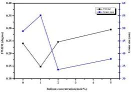
thin films deposited for various In dopant concentrations .The films are polycrystalline with hexagonal structure with preferred orientation along (100) plane up to In 2% .Further increase in In content (In 5%), intensity of (100) peak weakens and (002) crystal plane stars to grow leading to reorientation of the crystal [5] .When the concentration reaches 7.5% there is a hump at 31˚ and no peaks are observed indicating the amorphous nature of the films. At higher doping level insoluble In atoms segregate at the grain boundaries inhibit the growth of ZnO: In crystals [5] .The overall picture depicts the deterioration of crystallinity of the films, as the concentration grows. Variation of FWHM, grain size with different Indium content is shown in Figure 2(c).The grain size varies from 46nm to 55nm for undoped and In doped films.
[image:3.595.340.515.369.502.2]2.3 Optical properties
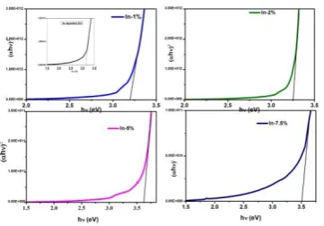
Fig. 3 (ahν)2 vs hν plot for as deposited(inset) and IZO
[image:3.595.74.255.379.505.2]thin films for different In dopant (mole % ).
Fig. 4 Variation of Refractive index for various In dopant (mole %)
The optical absorption studies show that maximum absorbance of all the films are less than 1.4 and found to decrease in the UV in the region. The absorption edges are blue shifted from 410nm to 407nm.Thereafter the absorption is constant in the visible and near IR region. The optical band gap calculated using Tauc's relation is given by,
αhν = A (hν -Eg)1/2
for direct allowed transition. This variation of (αhν)2 with
photon energy (hν) were plotted and it is shown in figure (3) with the undoped curve shown as the inset. The extrapolation of the linear portion of the curves to α = 0, gives the optical band gap energies. The optical band gap energies (Eg) for undoped to In doped ZnO films were found
to vary between 3.06eV to 3.6eV, According to Burstein -Moss effect, the optical band gap (Eg) should increase due to
the incorporation of In ions. Which is due to the shifting of Fermi level into the conduction band due to doping, in degenerate semiconductors [8] .The variation of refractive indices (n) with Indium concentration is shown in Figure (4) . The index of refraction was calculated from reflectance data and found to vary between 2.36 to 2.24 and In 5% posses he minimum value.
[image:3.595.351.505.567.684.2]Fig. 5 The optical transmission spectra of IZO for different In dopant (mole %).
Fig. 6 Photoluminescence Spectra thin films as deposited(inset) and IZO films for different In dopant
(mole %)
[image:3.595.109.212.568.651.2]© 2017, IRJET | Impact Factor value: 5.181 | ISO 9001:2008 Certified Journal | Page 195 transmiision, the films are found to be highly transparent
with maximum transparency obained for In 5% .The PL emission spectra of IZO films are shown in figure 6.The NBE emmission peaks for In-1% are more intense than 2% and 5% in the PL spectra.The blue emission at 462nm for In-1% is shifted to 456nm and the green emission at 506 nm shifted to 508 nm for higher Indium concentrations.A broad peak at 580 nm is absent for In-2% and In-5%.
2.3 Elecrical properties
The electrical properties of semiconducting oxide films depend on doping effect and also it’s deviation from the stochiometry [1].The elecrical properties of IZO thin films are summarized in table 1. The resisitiviy ρ is calculated by ρ = Rs d where Rs the sheet resistance and d is the thickness of the film. The ZnO thin film doped with In 1% has minimum resistiviy compared with other IZO films. Conductivity could not be measured for IZO 7.5% .This may be due heavy doping, where there is an enhancement of grain boundary scattering resulting from ZnO lattice disorder [3].
Table -1: The electrical properties of Indium doped Zinc oxide thin films
In Concentr ation (mole %) Sheet resista nce 103 (Ω
□-1)
Figur e of merit (φ) 10-2 Resist ivity ρ(Ω cm) Thic knes s (µm) Conduct ivity (S cm-1)
0 22.65 0.30 45.07 1.99 0.22
1 8.87 0.76 10.12
x10-2
1.15 0.99
2 7.02 1.10 13.05
x10-2
1.86 0.76
5 7.61 0.88 21.84
x10-2
2.87 0.48
For optoelectronic device applications, the figure of merit (φ) of the films plays an important role. The device performance is determined from φ and is calculated by using the formula
Where T10 is the transmittance at 550 nm and
Rs is the sheet resistance. The figure of merit for the IZO
films deposited for various concentrations are listed in Table 1.The figure of merit (φ) increases with doping and then it falls for heavy doping. The highest value of figure of merit
1.10 x 10⁻²□ Ω -1is obtained for In2% films which is higher
than value reported (1.5 x10⁻⁴□ Ω -1 ) for Indium doped films.
[5]. Doping reduces the resistivity of the films from 45.07Ω cm (undoped ZnO) to a minimum of 0.10 Ω cm( In doped ZnO), which may be due to the replacement of Zn 2+ ions by
In 3+ ions in the Zn lattice. This provides extra electrons for
conduction thereby increasing the conductivity of the IZO thin films. As reported by Hadri et.al it is shown that Indium content is a factor that affects the electrical properties.[8]
3. CONCLUSIONS
The effect of Indium dopant on structural, optical and electrical properties of ZnO thin films was investigated. The IZO films are polycrystalline and doping reorients the crystal plane from (100) to (002) plane. SEM micrographs reveal the nano fibrous structure with a average width of the nano fibre as 440nm.The optical band gap varies from 3.06eV to 3.6eV due to doping. The average transmittance of the films are 80% in the visible region. The highest value of figure of merit 1.10 x 10⁻² □ Ω -1 was obtained for 2% IZO films. The
resistivity of the films decreases from 45.07Ω cm for the undoped to a minimum of 0.10 Ω cm (In 1%) for the doped samples. These IZO films synthesized by spray pyrolysis can be good contenders for the application as the transparent electrode in solar cell.
ACKNOWLEDGEMENT
The author would like to thank the University Grant Commission, India for the grant provided under Faculty development program.
REFERENCES
[1] Benny Joseph, P K Manoj and V K Vaidyan “ Studies on preparation and characterization of indium doped zinc oxide films by chemical spray deposition” Bull. Mater. Sci., Vol. 28, No. 5, August 2005,pp. 487-493.
[2] S. Edinger , N. Bansal1, M. Bauch1, R. A. Wibowo1, G. U´ jva´ ri1, R. Hamid2, G. Trimmel,and T. Dimopoulos, “ Highly transparent and conductive indium-doped zinc oxide films deposited at low substrate temperature by spray pyrolysis from water-based solutions” J Mater Sci (2017) 52:8591–8602
[3] Joon Ho Bang , Se Hun Park, Sang Hyun Cho, "Properties of Indium Doped Zinc Oxide Thin Films Deposited by Magnetron Sputtering" Research Gate J. Kor. Inst. Surf. Eng. Vol. 43, No. 4, 2010.
© 2017, IRJET | Impact Factor value: 5.181 | ISO 9001:2008 Certified Journal | Page 196 doped Zinc oxide thin films Deposited by Chemical Spray
Technique, Starting from Zinc Acetaylacetonate and Indium Chloride" Materials 2014, 7, 5038-5046; doi:10.3390/ma7075038
[5] S S Shinde, P S Shinde, C H B hosale and kK Y Rajpure "Optoelectronic properties of sprayed transparent and conducting indium doped zinc oxide thin films" IOP Publishing j.Phys: D: Appl.Phys.41 (2008) 105109
[6] Rajesh Biswal, Luis Castaneda ,Rosario Moctezuma, JaimeV ega-Perez "Formation of Indium doped Zinc oxide thin films by Ultrasonic Spray Pyrolysis:The importance of water content in the aerosol solution and substrate temperature for enhancing electrical transport Materials 2012 , 5,432-442; doi: 10.3390/ 5030432
[7] Karmvir Singh , Rakesh Dhar , Devendra Mohan "Synthesis and characterization of Aluminum and Indium co-doped Zinc oxide thin fims prepared by Pulsed Laser deposition" j Integr Sci Technol , 2016, 4(1), 33-36
[8] .Hadri, C.Nassiri, F.Z.Chafi, M.Loghmarti, B.Fares, L.Laanab, F. Chraibi, M,Bensitel, A.Mzaerd " Indium doped Zinc oxide thin films: Effect on structural, optical and electrical properties of sprayed ZnO thin films" Sensors & Transducers, Vol. 178,Issue 9, September 2014, pp.63-68.
BIOGRAPHIES
Mrs.A.Jacquiline Regina Mary, Asscoicate Professor of Physics has 27 years of teaching experience in Jayaraj Annapackiam college for women, Periyakulam. Area of specialization is thin film solar cell .