© 2017, IRJET | Impact Factor value: 5.181 | ISO 9001:2008 Certified Journal | Page 2068
UNIVERSAL VERIFICATION METHODOLOGY BASED VERIFICATION
ENVIRONMENT FOR PCIE DATA LINK LAYER
Dr.T.C.Thanuja
[1], Akshata
[2]Professor, Dept. of VLSI Design & Embedded systems, VTU, Belagavi, Karnataka, India
[1]PG Student, Dept. of VLSI Design & Embedded systems, VTU, Belagavi, Karnataka, India
[2]---***---
Abstract
—
In today’s industry design complexity increased with the number of transistors hence enhance the verification complexity. Chip designer need to spend 70% of design time and size of code get reduces so efforts for verification .Peripheral component interconnect express data link layer is serial, I/O interconnect and high speed communication protocol. PCIE is layered and packets based transition protocol. Generation of different packets, flow control initialization, retry mechanisms and LCRC error check and data integrity are some of properties of Data Link Layer [DLL]. In this paper main aim is verification of all properties of data link layer using UVM And achieving the coverage goals. All these properties of DLL are verified with the aid of universal verification methodology and using Questa sim tool. The performance of verification is enhancing using modularity, reusability, and overriding mechanisms.UVM code is written by using UVM 1.1source object.Keywords—PCIE (Peripheral component Interconnect Express), UVM (Universal verification Method), Retry Mechanism, Questasim.
1. INTRODUCTION
Recently manufactured systems on chip designs are highly complex and expensive for verification of each design. At present verification engineers are using simulation based method for verification. The main challenges in verification are to verifying the design without losing the properties of coverage circuit should verified on time to market with less cost. There are many verification methods such as functional verification, assertion based verification, Formal verification. The main topic of focus is the functional verification of PCI Express protocol using universal verification methodology. PCI Express is point to point, serial protocol, high speed bus, and a switch based topology is used for transaction. Data is transferred in terms of packet. There are three layers in. Transaction layer, data link layer and physical
layer. These layers are
similar to that of
OSI model layers and all
services are
merged into three layers instead of seven layers. In
this paper mainly focusing on data
link layer services and verification of it. For verification of data link layer three interfaces needed to create, so that writing universal verification component for each interface. Each UVC has a monitor, test, environment, sequence, driver etc. PCIE 3.0specifications are used and which are introduced by PCI SIG.
2. OVERVIEW OF PCIE
The PCI bus clock has a frequency of 33MHz and the address bus width is 32-bits (4GB memory address space), although PCI optionally supports64-bit address bus. The data bus width is implemented as either 32-bits or 64-bits depending on bus performance requirement. The address and data bus signals are multiplexed on the same pins (AD bus) to reduce pin count .PCI is introduced by INTEL,PCI– SIG in1993.The maximum frequency achievable with the PCI architecture is 66 MHz this is a result of the static clock method of driving and latching signals. PCI bus efficiency is in the order of 50% to 60%.The PCI specification all own master and target devices to insert wait-states during data phases of a bus cycle.
Slow devices will increases wait-states which will reduces the efficiency of bus cycles. PCI bus cycles do not indicate the transfer size. This makes buffer management within master and target devices inefficient .Delayed transactions on PCI are handled inefficiently. When a master is retried, it guesses when to try again PCI interrupt than dling architecture is in efficient specially because multiple devices share a PCI interrupt signal. Additional software latency is incurred when software discovers which device /devices that share an interrupt signal actually generated the interrupt.
© 2017, IRJET | Impact Factor value: 5.181 | ISO 9001:2008 Certified Journal | Page 2069 background noise but it has faster a bus runs. For this
reason manufacturing standards for high-speed buses are exceptionally strict and therefore expensive. PCI Express implements switch-based technology to interconnect a large number of devices. Communication over the serial interconnections is accomplished using a packet-based communication protocol. Quality Of Service(QoS) features provides differentiated trasmission performance for
different applications. Hot Plug/Hot Swap support
enables "always-on" systems. With advanced power
management features it can be used to design for low
power mobile applications. RAS (Reliable, Available
,and Serviceable)error handling features make PCI
Express suitable for robust high-end server
applications. Hot plug, power management, error
handling and interrupt signaling are accomplished
in-band packet based messaging rather than side-in-band
signals. This keeps the device pin count low and also
reduces system cost.
3. LAYERED ARCHITECTURE Data Link Layer
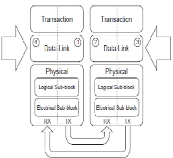
[image:2.595.345.546.111.176.2]PCIE express has its application in many fields such as communication platform and computing field .figure 1 shows the layered diagram for PCI-E data link layer. Transaction layer is top most layer and physical layer is final layer. Data link layer is middle layer.
Figure 1. Layering figure of PCIE data link layer.
[image:2.595.367.520.205.382.2]Data link layer packets are generated in the data link layer and those packets are transferred from data link layer of PCIE device A to data link layer of PCI express layer device B. Figure 2 shows the packet formation in the each layer. Data link layer packet format consists sequence of 2 byte, header of 4 data word, ECRC of 2Dw and LCRC 1Dw. Data link layer packet can be formed by adding sequence number and link cyclic redundancy to check the transaction layer packet.
Figure 2.Packet Format of PCIE State Machine for Data Control
Figure 3.State machine diagram for data link control
SATES:
[1] DL-INACTIVE: Physical Layer reporting link is Non-working that is nothing is connected,
[2] DL-INIT: Physical Layer reports that linkis ON, initialize flow control for the default Virtual channel
[3] DL-ACTIVE: Common operation mode.
STATUS OUTPUT :
[a]DL- Down: Data Link Layer is not conveying With the component on another side of the link.
[b] DL-UP: Data Link Layer is communicating within the other side of the link.
4 .METHODOLOGY AND IMPLEMENTATION
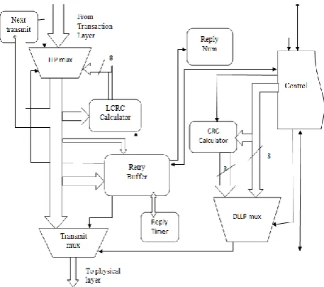
The data link layer architecture consists of two parts. One is the transmitter and another one is receiver. Transmitter is nothing but PCIE device A and which takes data in terms of packets from the transaction layer and adds 16 bit sequence number to those packets through next transmit seq. next transmit sequence is 12bit counter. As shown in figure 4
[image:2.595.86.260.450.609.2]© 2017, IRJET | Impact Factor value: 5.181 | ISO 9001:2008 Certified Journal | Page 2070 out then retry buffer sends negative acknowledgement. If
negative acknowledgement is receive then need to resend the packets. If packets are positive acknowledged then packets are send to transmit mux. Control is major block of transmitting part of the data link layer. It gives information about when to connect with transaction layer and when to connect with physical layer. This is called as link management operations. Control also gives information about whether buffer space is available in the other layer or not and when to do retry mechanism. Reply number is 2bit counter, it counts number of times retransmission had been done. Finally both DLLPS and TLPS are sent to transmit mux. From transmit mux packets are send to physical layer.
Fig 5 shows the receiver device of PCIE DLL. Receiver is nothing but PCIE device B. Receiver data link layer receives the packets from the physical layer. DLLPs differentiator takes the packets from the physical layer and separates those packets into data link layer packets and transaction layer packet. It will send the TLPS to LCRC calculator check, which checks the packets are to see that whether LCRC values match to original packets LCRC value. If matched then LCRC calculator check sends the packets to RX buffer, if not it rejects the packets. Rx buffer is just like retry buffer (transmitter part) which stores the packets, It has sub module called sequence check. It checks sequences if not matched then takes the 8bit sequence from the next receiving sequence. Then scheduling for TLPs is done after that those packets are sent to transaction layer.
[image:3.595.338.571.79.316.2]Packets from DLLP differentiator are sends to CRC calculator again it calculates the CRC values with original packets if okay then it sends packets to control and control works in similar manner as it works in transmitter .ACK/NACK timer counts time taken for scheduling of TLPS
Figure 4. Transmitter part of Data Link Layer.
.
Figure 5. Receiver Part of Data Link Layer.
5. VERIFICATION
FRAMEWORK
[image:3.595.332.559.517.633.2]Figure 5 shows the test bench architecture for PCIE link layer using UVM. It is composed of five universal verification components (UVC). TL Receive Universal verification component for receiving the TLPs from the TL. Transaction layer transmit UVC for sending the Transaction layer packets to the TL. Physical layer transmit UVC for transmitting the DLLPs plus TLPs to the TL. Physical layer receiver UVC for accepting the DLLPs with TLPs from the PL. Advanced peripheral bus UVC is used for programming of register in DLL design. DUT is design under test.
Figure 5: Verification Environment
Test bench system has several parts including:
1. PCI Express data link layer design [DUT]
2. APB interface
3. Data link layer to physical layer interface
[image:3.595.45.274.525.727.2]© 2017, IRJET | Impact Factor value: 5.181 | ISO 9001:2008 Certified Journal | Page 2071 5. Data link layer environment
6. Sequence library and test library.
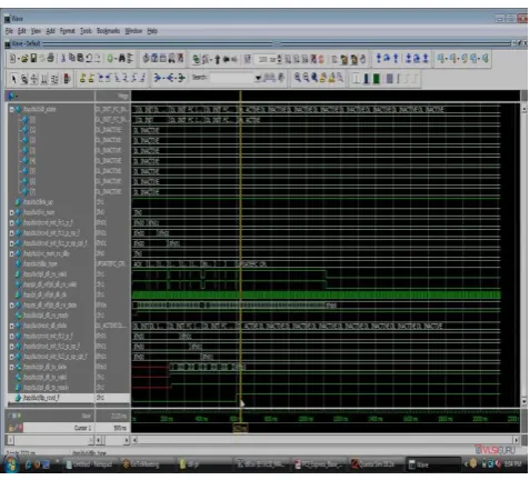
[image:4.595.314.567.99.290.2]6. RESULTS
Fig 6 shows that the data link management state machine is ON at which virtual channel among eight virtual channels and shows that through which virtual channel packets are transmitting and receiving.
Figure 6. DL_FC_VC_TEST.
Fig 7 shows that while transmit the packets if while if negative acknowledgement is received then retry packets are sent.
Figure7. DL_TLP_RETRY_TEST
Fig 8 shows that while sending the packets to buffer memory, if size of packets is bigger than the buffer space then overflow occurs. Here at virtual channel 2 overflows occurred.
[image:4.595.39.278.221.437.2]Figure 8.DLL_BUFFER_OVERFLOW_TEST
Fig 9 shows creation of some random TLPs and LCRC of random TLPS should match LCRC value of original TLPS then it will not shows any LCRC error. At VCO it is showing error because of mismatch of LCRC value.
[image:4.595.316.575.381.579.2]© 2017, IRJET | Impact Factor value: 5.181 | ISO 9001:2008 Certified Journal | Page 2072 Figure 10.UVM RESULT REPORT
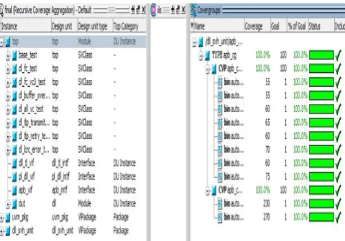
[image:5.595.37.288.361.536.2]Functional Coverage; how much percentage test plans are excersized in the verification enivornment can be decided by this FC factor.
Figure 11. Functional Coverage Report
7. CONCLUSION
A universal verification methodology based verification environment for PCIE data link layer is built. The verification system gives all interface and tools including coverage, enumeration software, and constraint random checker, agent, monitor and sequencer. Each component of verification system co-operates each other to form compliance test suits. DUT is completely verified by interfacing with other components in the verification system. Some properties of PCI express data link layer are verified, such as flow control initialization of all virtual channels, overflow and retry mechanism. Improved the performance of verification by using UVM 1.1 source object instead of VHDL, Verilog. The Reusable, modular verification environment is created; hence time taken for verification and efforts are getting reduced.
In future remaining all properties of PCIE can be verified. Verification can be carried out by UVM 1.2 object source. Can also achieve high throughput by increasing the bandwidth and redesigning the physical layer
ACKNOWLEDGEMENT
I am highly indebted to Dr. T.C Thanuja guide and head of department of VLSI design and embedded system, VTU, PG center Belagavi for motivation and advice and giving useful suggestions for project. I am thankful to co-guide Mr. Rohit Malagi. I am very grateful for my college, all professors and lab workers and who supported me carrying this work.
REFERENCES
[1] PCI Express Base Specification, http://www.pcisig.com [2] “PCI Express® Base Specification Revision 3.0 November10, 2010”.
[3] H. Kavianipour, S. Muschter, and C. Bohm, “High performance FPGA based DMA interface for PCIE,” IEEE Trans. Nucl. Sci., vol. 61, no.2, pp. 745–749, Apr. 2014. [4] M. Aguilar, A. Veloz, M. Guzman, “Proposal of Implementation of Data Link Layer of PCI-Express”, First International Conference on Electrical and Electronic Engineering,2004