International Journal of Emerging Technology and Advanced Engineering
Website: www.ijetae.com (ISSN 2250-2459, ISO 9001:2008 Certified Journal, Volume 3, Issue 6, June 2013)
96
A 3GHz Low-offset Fully Dynamic Latched Comparator for
High-Speed and Low-Power ADCs
Shaik Mastan Vali
1, Pyla Rajesh
2 1Associate Professor, Department of ECE, MVGR College of Engineering, Vizianagaram, India 2M.Tech-VLSI Student, Department of ECE, MVGR College of Engineering, Vizianagaram, India
Abstract—In this paper, performances of various types of
dynamic latched comparators are compared in terms of their offset voltages, speed and power. The accuracy of comparators, which is defined by its offset, along with power consumption, speed is of keen interest in achieving overall higher performance of ADCs. This can be achieved by the fully dynamic latched comparator which is proposed in this paper. This comparator shows 14.6mV offset which is small when compared to other dynamic comparators and pre-amplifier based comparators. This comparator not only achieves low-offset but also exhibit high-speed and low power in its operation, which can be used for low power high speed ADC applications.
Keywords—ADC, Fully dynamic, Input-referred offset
voltage, Latched Comparator, Pre-amplifier
I. INTRODUCTION
Comparators have a crucial influence on the overall performance in high-speed analog-to-digital converters (ADCs). Since they are decision-making circuits that interface the analog and digital signals, the accuracy, which is often determined by its input-referred offset voltage, is essential for the resolution of high-performance ADCs. Dynamic comparators are widely used in high-speed ADCs due to its low power consumption and fast speed.
They use positive feedback mechanism with one pair of back-to-back cross coupled inverters [4] in order to convert a small input-voltage difference to a full-scale digital level in a short time. However, an input-referred latch offset voltage, resulting from static mismatches such as threshold voltage Vth and ß variations in the regenerative latch,
deteriorates the accuracy of such comparators. Moreover, dynamic mismatch from the unbalanced parasitic capacitances [4] on the output nodes of the latch causes the additional offset term during evaluation phase. Because of this reason, the input-referred latch offset voltage is one of the most important design parameters of the latched comparator. If large devices are used for the latching stage, a low offset can be achieved at the cost of the reduced speed due to slowing the regeneration time and the increased power dissipation.
In this paper, we present a new dynamic latched comparator which shows lower input-referred latch offset voltage and higher load drivability than the conventional dynamic latched comparators. Even though numbers of transistors in the proposed comparator are more but overall area is small when compared to conventional dynamic latched comparators.
This paper is organized as follows. Section II provides an overview of the various types of dynamic latched comparators in terms of their advantages and drawbacks, and section III describes the offset analysis of proposed dynamic latched comparator. Section IV provides schematics of various types of dynamic latched comparators which are drawn in T-Spice. Simulation results from HSPICE using 90nm PTM technology with
VDD=1V and their comparisons are presented in Section V
and conclusion is drawn in Section VI.
II. DYNAMIC LATCHED CMOSCOMPARATORS A.Design considerations of comparators
Design considerations [10] for voltage comparators are can be summarized as high-speed (maximum clock rate fs, which is related to small signal bandwidth, slew rate, and settling time), accuracy (high-resolution, which is related to gain, offset voltage, RMS and kickback noise, overdrive recovery, and linearity of input capacitance), wide input common–mode range, CMR (common-mode rejection), low-power consumption, small-area and so on.
More practically, the input-referred latch offset voltage can be reduced by using the pre-amplifier preceding the regenerative output-latch stage as shown in Figure 1. Pre-amplifier based latched comparator is a combination of a pre-amplifier and a latch. It can amplify a small input voltage difference to a large enough voltage to overcome the latch offset voltage and also can reduce the kickback noise. However, the pre-amplifier based comparators suffer not only from large static power consumption for a large bandwidth but also from the reduced intrinsic gain with a reduction of the drain-to-source resistance rds due to the
International Journal of Emerging Technology and Advanced Engineering
Website: www.ijetae.com (ISSN 2250-2459, ISO 9001:2008 Certified Journal, Volume 3, Issue 6, June 2013)
[image:2.612.65.277.125.272.2]97
Figure 1: Pre-Amplifier based latched comparatorThe pre-amplification stage of the conventional comparator can be removed in order to reduce silicon area by using dynamic latch comparators.
B. Previous works
Lewis-Gray Comparator [8] has low DC power consumption and adjustable threshold voltage. The transconductance of transistor M3 and M4 is much larger than that of the input transistor pair; hence the differential voltage gain built between Di nodes from the input transistor pair is not big enough to overcome an offset voltage caused from such a small mismatch between transistor M3 and M4 pair. As a result, those transistors are the most critical mismatch pair in this comparator and needed to be sized big enough to minimize the offset voltage at the cost of the increased power consumption. Lewis-Gray comparator shows a high offset voltage and its high offset voltage dependency on a different common mode voltage Vcom, it is only suitable for low resolution
comparison.
Comparing with Lewis-Gray comparator, Differential pair comparator [8]shows faster operation and less overall offset voltage. However, still its structure which consists of a stack of 4 transistors requires large voltage headroom; it is problematic in low-voltage deep-submicron CMOS technologies. Strong dependency on speed and offset with a different common-mode input voltage Vcomand problem in
low power supply voltage operation due to its structure can be overcome by using Double-tail latch-type voltage SA [2]. Since this comparator requires both Clk and Clkb
signals for its operation, high accuracy timing between Clk
and Clkb is required otherwise desired output may deviate and it results in increased power dissipation. The comparator from [3] without offset calibration technique resolved the problem by replacing Clkb with Di nodes.
As a result, Clk load was lessened and the input-referred offset was reduced because the output latch-stage obtains the gain from the both second-input transistor pairs (M10/M11 and M12/M13). However, the improved offset has to trade off with the increased delay.
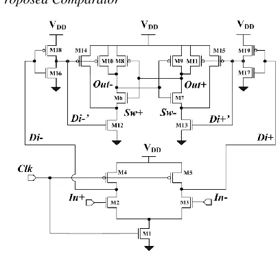
[image:2.612.338.542.205.394.2]C.Proposed Comparator
Figure 2: Proposed comparator
The proposed comparator provides better input offset characteristic and faster operation in addition to the advantages of those comparators such as less kickback noise, reduced clock load and removal of the timing requirement between Clk and Clkb over a wide common-mode and supply voltage range. The overall area is small even though number of transistors is more. It is because of widths of transistors are optimized without compromising the speed and performance of the comparator. The below table shows the transistor lengths and widths of proposed comparator.
TABLE I
LENGTHS AND WIDTHS OF TRANSISTORS
International Journal of Emerging Technology and Advanced Engineering
Website: www.ijetae.com (ISSN 2250-2459, ISO 9001:2008 Certified Journal, Volume 3, Issue 6, June 2013)
98
For its operation, during the pre-charge (or reset) phase (Clk=0V), both PMOS transistor M4 and M5 are turned on and they charge Di nodes’ capacitance to VDD, which turn
both NMOS transistor M16 and M17 of the inverter pair on and Di’ nodes discharge to ground. Sequentially, PMOS transistor M10, M11, M14 and M15 are turned on and they make Out nodes and SW nodes to be charged to VDD while
both NMOStransistors M12 and M13 are being off. During the evaluation (decision-making) phase (Clk=VDD), each Di
node capacitance is discharged from VDD to ground in a
different time rate proportionally to the magnitude of each input voltage. As a result, an input dependent differential voltage is formed between Di+ and Di- node. Once either
Di+ or Di- node voltage drops down below around
VDD−|Vtp|, the additional inverter pairs M18/M16 and
M19/M17 invert each Di node signal into the regenerated
Di’ node signal. Then the regenerated and different phased
Di’ node voltages are amplified again and relayed to the output-latch stage by transistor M10−M13. As the regenerated each Di’ node voltage is rising from 0V to VDD
with a different time interval, transistor M12 and M13 turn on one after another and the final amplification is made between SW nodes before the regeneration process. Once either of SW node voltages falls below around VDD−Vtn, the
output latch stage starts to regenerate the small voltage difference at Out nodes into a full-scale digital level.
III. OFFSET ANALYSIS OF PROPOSED COMPARATOR
To further reduce the offset voltage of the proposed comparator, it is necessary to find the most critical mismatch transistor pair first. Since transistor M2 and M3 pair is the input transistors and starts to operate in the saturation region during evaluation phase, they are the most critical mismatch pair for the total offset voltage and the offset voltage caused by the mismatch between them can be expressed as
( - ) {(
) (
) } (
) (1) If a mismatch exits in the output latch stage, the circuit will be unbalanced making Vout+(t) ≠ Vout−(t). In order for the circuit to be balanced, a voltage VOS, latch should be
applied between the output of the inverter (M18/M16) and
Di-’ node to compensate the mismatch when Di’ nodes rises. In order to calculate the offset voltage VOS, latch of the output stage, the mismatch in current factor β and threshold voltage Vth are assumed to be the dominant
factors to cause the offset voltage for our analysis. The offset voltage caused by the mismatch between M12 and M13 can be expressed as
[( - ) ( ) ] { - ( - - | |)* +} - (2)
For mismatch between transistor M6 and M7, from the fact that ID12 = ID6and ID13 =ID7, we have
[( ) ( - - ) ( - ) ] (3)
In a similar way, the offset voltage VOS10,11 caused by the
transistor mismatch between M10 and M11 can be found
( ( ) ( - - | |)) , ( - - | |) ( - )-- (4)
Where ( ) ( )
To calculate the offset voltage caused from the capacitance mismatches at Out nodes (which includes the load capacitance and parasitic capacitance), it is necessary to assume that
CL1 = C and CL2 = C + ΔC
The offset voltage caused by the capacitance mismatch at between the output nodes is
( - ) ( ) { - ( - - | |)* +} - (5)
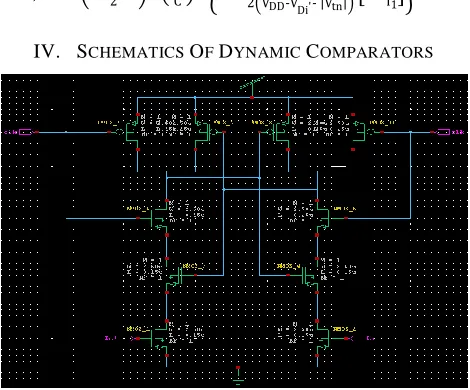
[image:3.612.327.562.470.665.2]IV. SCHEMATICS OF DYNAMIC COMPARATORS
International Journal of Emerging Technology and Advanced Engineering
Website: www.ijetae.com (ISSN 2250-2459, ISO 9001:2008 Certified Journal, Volume 3, Issue 6, June 2013)
[image:4.612.55.286.130.301.2] [image:4.612.326.564.132.350.2]99
Figure 4: Latch type voltage sa comparator (comparator2) [image:4.612.53.287.324.548.2]Figure 5: Dual-tail latch-type voltage SA comparator (comparator3)
Figure 6: Two stage dynamic comparator (comparator4)
[image:4.612.325.563.373.598.2]International Journal of Emerging Technology and Advanced Engineering
Website: www.ijetae.com (ISSN 2250-2459, ISO 9001:2008 Certified Journal, Volume 3, Issue 6, June 2013)
100
V. SIMULATION RESULTS
To compare the performances of the proposed comparator with the previous works, each circuit was designed using 90nm PTM technology with VDD=1V,
fclk=3GHz, Cload=7fF, Temp=250C, and common mode
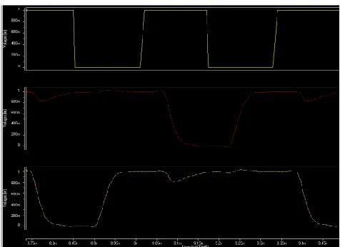
[image:5.612.324.563.131.309.2]voltage Vcom=0.7V and simulated with HSPICE. A.Simulated Waveforms
[image:5.612.51.290.229.407.2]Figure 8: Simulated waveforms for comparator1
[image:5.612.325.565.323.506.2]Figure 9: Simulated waveforms for comparator2
Figure 10: Simulated waveforms for comparator3
Figure 11: Simulated waveforms for comparator4
[image:5.612.53.288.432.610.2] [image:5.612.325.563.529.702.2]International Journal of Emerging Technology and Advanced Engineering
Website: www.ijetae.com (ISSN 2250-2459, ISO 9001:2008 Certified Journal, Volume 3, Issue 6, June 2013)
101
[image:6.612.44.297.162.416.2]B.Performance Comparison
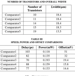
TABLE II
NUMBER OF TRANSISTORS AND OVERALL WIDTH
Number of Transistors
Σwidth(µm)
Comparator1 10 18.4 Comparator2 11 18.4 Comparator3 14 18.4 Comparator4 15 18.3 Comparator5 19 13.5
TABLE III
SPEED, POWER AND OFFSET COMPARISONS
Delay(ps) Power(mW) Offset(mV)
Comparator1 103 0.118 51 Comparator2 82 0.135 32 Comparator3 70 0.193 19.4 Comparator4 88 0.159 15.8 Comparator5 77 0.133 14.6
VI. CONCLUSION
In this paper, we present a new low power dynamic latched comparator which shows lower offset voltage and higher output load drivability over the conventional dynamic latched comparators. It shows 14.6mV offset voltage and 0.133mW power, which is suitable for low power high speed ADCs.
REFERENCES
[1] Wicht, T. Nirschl, and D. Schmitt-Landsiedel, “Yield and speed optimization of a latch-type voltage sense amplifier,” IEEE J. Solid-State Circuits, vol. 39, pp. 1148-1158, July 2004.
[2] Schinkel, E. Mensink, E. Kiumperink, E. van Tuijl and B. Nauta, “A Double-Tail Latch-Type Voltage Sense Amplifier with 18ps Setup+Hold Time,” ISSCC Dig. Tech.Papers, pp. 314-315 and 605, Feb. 2007.
[3] M. Miyahara, Y. Asada, P. Daehwa and A. Matsuzawa, “A Low-Noise Self-Calibrating Dynamic Comparator for High-Speed ADCs,” in Proc. A-SSCC, pp. 269-272, Nov. 2008.
[4] Nikoozadeh and B. Murmann, “An Analysis of Latch Comparator Offset Due to Load Capacitor Mismatch,” IEEE Trans. Circuits Syst. II: Exp. Briefs, vol. 53, no. 12, pp. 1398-1402, Dec. 2006 Philip E. Allen and Douglas R. Holberg, CMOS Analog Circuit Design, 2nd ed. New York, NY: Oxford, 2002.
[5] S. Kale and R. S. Gamad, “Design of a CMOS Comparator for Low Power and High Speed,” Internationl Journal of Electronic Engineering Research, vol. 2, no. 1, pp. 29-34, 2010
[6] Pedro M.Figueiredo, Joao C.Vital, “Kickback Noise Reduction Techniques for CMOS Latched Comparator”, IEEE Transactions on Circuits and Systems, vol.53, no.7, pp.541- 545, July 2006. [7] 90nm Predictive Technology Model (PTM),
[Online]Available:http://www.eas.asu.edu/~ptm/latest.htm [8] Sumanen, M. Waltari, V. Hakkarainen, K. Halonen, “CMOS
Dynamic Comparators for Pipeline A/D Converters,” IEEE ISCAS, vol. 5, pp. 157 - 160, May 2002.
[9] Jeon, Heung Jun, "Low-power high-speed low-offset fully dynamic CMOS latched comparator" (2010).
International Journal of Emerging Technology and Advanced Engineering
Website: www.ijetae.com (ISSN 2250-2459, ISO 9001:2008 Certified Journal, Volume 3, Issue 6, June 2013)
102
AUTHOR BIOGRAPHYShaik Mastan Vali received his B.Tech degree from Nagarjuna University in the year 1996 and received M.E degree from Andhra University in the year 2000. He is a Ph.D scholar and he is working as an Associate Professor in the Department of Electronics and Communication Engineering at MVGR College of Engineering. He has published many papers in National and International Conferences and reputed journals