N A N O E X P R E S S
Open Access
First-Principles Study on the Stability and
STM Image of Borophene
Zhifen Luo, Xiaoli Fan
*and Yurong An
Abstract
Very recently, borophene (atomic-thin two-dimensional boron sheet) has been successfully synthesized on the Ag(111) surface by deposition. Two kinds of structures were found. However, the identification of the monolayer boron sheets grown on the metal substrate, as well as the stability of different 2D boron sheets, is controversial. By performing the first-principles calculations, present study investigates the atomic structure, stability, and electronic properties of the most possible boron sheets grown on metal surface, namely, buckled triangular,β12, andχ3types of crystal lattice. Our
result shows that all the three freestanding sheets are thermodynamically unstable and all are metallic. On the other hand, our result indicates the Ag(111) substrate stabilize these sheets. Additionally, our simulated STM images of these monoatomic-thin boron sheets on Ag(111) surface reproduce the experiment observations well and clearly identify the as-grown boron sheets.
Keywords:Atomic-thin boron sheet, First-principles calculations, Atomic structure, Stability, STM image
Background
Since the discovery of graphene, two-dimensional (2D) materials have become one of the most active nanoma-terials due to their unique physical properties and poten-tial applications in next-generation electronics and energy conversion device [1–7]. Recently, a class of 2D boron nanostructures has been discovered and attracted significant attentions [8–21]. However, there was no evi-dence that the 2D boron sheets could be realized experi-mentally until very recently, both Mannix et al. [22] and Feng et al. [23] made spectacular advances in realizing experimentally the atomic-thin 2D boron sheets. The ex-tended 2D boron sheet is called“borophene”, in analogy to graphene.
During the last two decades, numerous 2D boron nanostructures have been discovered [8–21]. Besides the hexagonal sheet and the triangular sheet [20, 21], as well as the buckled triangular sheets [8], other 2D boron sheets with hexagonal holes, like the α-sheet [9, 18], β -sheet [9, 18], γ-sheet [19], and g1/8 and g2/15 sheets [15], were examined by the ab initio calculations. It was suggested that the triangular planar boron lattice with
hexagonal vacancies is more stable [9]. And a variety of such triangular boron layer with different patterns of hexagonal holes were reported by both the computa-tional and experimental research groups [11, 13–16]. However, all of these monoatomic-thin boron layers are higher in energy than boron’s three-dimensional (3D) bulk state, which means that the 2D structure of boron is disadvantaged thermodynamically. Thus, a sufficiently “sticky” substrate is necessary to suppress the 3D nucle-ation barrier to entice the atoms into the 2D route.
Recently, the formation of boron sheets on metal and metal boride substrates has been explored by first-principles calculations [24]; it suggests that the boron sheets can be grown on the Ag(111) and Au(111) sur-face. Additionally, Piazza et al.’s [14] study provide ex-perimental evidence that the monolayer boron sheets are achievable based on their observations of B36cluster;
it was shown to be a highly stable planar cluster with a central hexagonal hole [14]. More recently, two groups [22, 23] successfully synthesized the atomic-thin, crystal-line 2D boron sheets on a silver surface by directly evap-orating a pure boron source via molecular beam epitaxy.
Mannix et al. [22] found two distinct phases of the boron sheet on silver substrate using high-resolution scanning tunneling microscopy (STM) characterization: a striped phase and a homogeneous phase. Feng et al.
* Correspondence:[email protected]
State Key Laboratory of Solidification Processing, School of Material Science and Engineering, Northwestern Polytechnical University, 127 YouYi Western Road, Xi’an, Shaanxi 710072, China
The exact configurations and properties, as well as the applications of these 2D boron sheets, have attracted tre-mendous attentions [19, 22, 24, 25]. It was reported that the buckled triangular borophene is a highly anisotropic metal with a high Young modulus along its armchair dir-ection which exceeds that of graphene [22]. Sun et al. also found that the lattice thermal conductivity of the buckled triangular borophene is strongly anisotropic [26]. More-over, Gao et al. reported that the β12 borophene and χ3
borophene may be another superconducting phase of boron besides MgB2thin film [27]. However, the
thermo-dynamic stability ofβ12borophene andχ3borophene are
controversial [27, 28]. According to Gao et al.’s study, both
β12 borophene and χ3 borophene are stable [27]. But
Penev et al. reported that bothβ12borophene andχ3
bor-ophene have imaginary frequencies near the G point in their phonon spectrums [28].
To provide a better understanding for the experimen-tal achievable borophene, we systematically investigated the possible atomic structures and their stability, as well as the electronic properties by performing the first-principles calculations. Our results indicate thatβ12and
χ3 sheets are thermodynamically unstable. Additionally,
the configurations of buckled triangular, β12, and χ3
sheets all show metallic feature. Moreover, we have sim-ulated the STM images for the freestanding and epitaxial monolayer of boron on the Ag(111) surface; we found buckled triangular andβ12boron sheets on Ag(111)
sur-face both look as stripe phases but with little difference.
Computational Methods
The calculations are performed by using the Vienna ab-initio simulation package (VASP) based on density func-tional theory (DFT) [29, 30]. The projector-augmented-wave method was adopted for the calculations of elec-tron–ion interactions [31, 32]. And the electronic ex-change–correlation interactions were described by the generalized gradient approximation (GGA) using the Perdew–Burke–Ernzerhof (PBE) functional [33]. Wave functions were expanded in a plane wave basis with an energy cutoff of 500 eV. The first Brillion zone were sampled by 25 × 15 × 1, 15 × 9 × 1, and 11 × 11 × 1 k-mesh for the buckled triangular, β12, and χ3 phases of
borophene, respectively. To simulate the 2D boron
The STM images were simulated using the Tersoff– Hamann formula and its extension [35]. Briefly, assum-ing that the density of states of the tip is constant, we can approximate the STM tunneling current with the local density of states,ρ!r;E, as the only variable with the following expression:
I Vð Þ∝
Z EFþeV
EF
ρ!r;EdE
ρ!r;E¼X
i
ψi !r 2
δðE−EiÞ
where ρ!r;E is the LDOS on the sample surface, ψi
r
! is the sample wave function with energyE
i, and EF is the Fermi energy. When the states in ρ!r;E are filled, it is also common to refer to ρ!r;E as the charge density of the states. The simulated STM images were obtained using the constant current mode based on calculated electron densities.
Results and Discussion
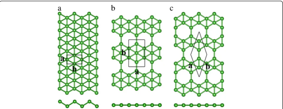
Figure 1 shows our calculated results for the buckled triangular, β12, and χ3 lattice structures of borophene.
Unlike the one-atom thin and planar hexagonal config-uration of graphene, buckled triangular borophene shows buckling along one lattice direction. On the other hand, the structures ofβ12and χ3borophenes are planar
without out-of-plane buckling. Figure 1a shows that there are two boron atoms in the unit cell of buckled triangular borophene. And the space group of buckled triangular borophene is Pmmn. Our optimized lattice constants area= 1.613 Å andb= 2.866 Å, agreeing well with previous theoretical and experimental results [22]. The β12 borophene shown in Fig. 1b has filled and
empty hexagons along the zigzag direction; the corre-sponding space group is P2mm. There are five boron atoms in the unit cell. The lattice constants are 2.916 and 5.075 Å along the a and b directions. The unit cell of χ3 borophene is rhombic, having four boron
As shown in Fig. 1, there are vacancies in bothβ12andχ3
sheets but not in the buckled triangular lattice and the number of vacancies inβ12and χ3borophene is different.
The vacancy concentration η is defined as the ratio be-tween the number of vacancy sites and total sites (including vacancy) in the unit cell; it is a quantity describing the boron sheets from global and local points of view [9].ηis 1/6 inβ12lattice and 1/5 inχ3lattice. Compared to theβ12
lattice, Fig. 1c shows that the neighboring vacancy rows in
χ3borophene are shifted by half of the lattice constant in
zigzag direction, resulting in a planar of C2mm symmetry. We calculate the average energy of each boron atom using the following equation for the three structures and use it to compare the relative stability of the three struc-tures; this method has been applied in Ref. [23]
EFB ¼Eborophene=n
whereEboropheneandnare the energy and the number of boron atoms in one unit cell, respectively. Our calcu-lated results are summarized in Table2. It indicates that the β12 phase is the most stable, while the χ3 phase is the least stable with relative higher energy of 0.08 eV.
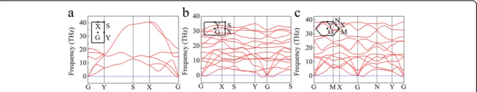
We then calculated the phonon dispersion spectrum for the three phases of buckled triangular, β12, and χ3
borophene. Figure 2 shows the phonon dispersion spec-trums along the high symmetry directions. As shown in Fig. 2a, there are three acoustic and three optical phonon branches for the buckled triangular borophene. It also shows imaginary values near the G point along the X–G direction, indicating that the lattice is unstable along thea direction, which explains the stripe formed along the a direction in the experimental STM images [23]. In fact, re-cent studies have suggested that the biaxial tensile and uniaxial tensile cannot stabilize the freestanding buckled triangular borophene even under the tensile stress of 0.08% [36, 37]. Figure 2b, c shows that there are also im-aginary frequencies near the G point ofβ12andχ3phases.
Our results show that all the three phases of buckled tri-angular,β12, andχ3are unstable.
We further studied the electronic structures of buckled triangular borophene, β12 borophene, and χ3borophene.
The calculated band structures along the high-symmetry directions are shown in Fig. 3. As shown in Fig. 3, all the three phases of buckled triangular,β12, andχ3borophenes
are metallic. Particularly, for the buckled triangular boro-phene as shown in Fig. 3a, three energy bands cross the Fermi level: one is along the S–Y direction and the other two are along the G–X direction. However, we have men-tioned in the above sections that the buckled triangular is buckling along theb direction, which opens a bandgap of
Fig. 1Top and side views of buckled triangular (a),β12(b), andχ3(c) boron sheets. The green balls represent the boron atoms. The rectangles and
[image:3.595.58.539.87.272.2]rhombus enclosed by solid black lines denote the unit cells. The lettersaandbrepresent the lattice parameter
Table 1Our calculated lattice constantsa,b, andγfor the buckled triangular,β12andχ3boron sheets. Previous results are
also listed for comparison
Previous studies Present result
a(Å) b(Å) γ a(Å) b(Å) γ
b△ 1.617 [22] 2.872 [22] 90° 1.613 2.866 90°
β12 2.922 [23] 5.057 [23] 90° 2.916 5.075 90°
[image:3.595.57.291.662.732.2]χ3 4.443 [27] 4.443 [27] 38.173° [27] 4.448 4.448 38.182°
Table 2Average energy for boron atoms in the freestanding (EFB) and epitaxial (EEB) boron sheets on the Ag(111)
Previous studies Present result
b△ β12 χ3 b△ β12 χ3 χ3’ EFB(eV/atom) / −6.23 [23] −6.19 [23] −6.19 −6.23 −6.15 −6.15
EEB(eV/atom) / −6.32 [23] −6.35 [23] −6.29 −6.33 −6.32 −6.35
[image:3.595.307.542.669.723.2]9.63 and 4.32 eV along the X–S and Y–G directions, re-spectively. It indicates that the buckled triangular boro-phene behaves as a metal with strong anisotropy and the electrical conductivity is confined along the uncorrugated adirection.
Additionally, we studied the atomic structures and sta-bility of the buckled triangular, β12, and χ3boron sheets
on the Ag(111) substrate. The results are shown in Fig. 4. The unit cell of buckled triangular borophene on Ag(111) surface is the (1 × 3) supercell of freestanding buckled tri-angular borophene and the recttri-angular 1 × (√3)R30° supercell of the Ag(111) substrate. For the configuration ofβ12sheet on the Ag(111) surface, the unit cell is the unit
cell of β12 borophene and 1 × (√3)R30° supercell of the
Ag(111) surface. Our calculations show that theβ12
boro-phene matches to Ag(111) surface (~ 1% mismatch) better than the buckled triangular borophene (~ 3% mismatch). The χ3 borophene forms two configurations on the
Ag(111) surface, as shown in Fig. 4c, d, which are named as χ3and χ3’. The unit cell ofχ3is rhombus with lattice
constant ofa = 8.67 Å, and the unit cell ofχ3’ is
ortho-rhombic with lattice parameters of a = 2.89 Å and b = 25.02 Å; it is the 1 × (5√3)R30° supercell of the Ag(111) surface.
According to our calculations, the vertical distances from the Ag(111) surface to the lower and upper boron atomic layers of the buckled triangular borophene are 2.5 and 3.3 Å, respectively, indicating the weak inter-action between the boron sheet and the Ag substrate. The
β12, χ3, and χ3’ sheets all remain planar on the Ag(111)
surface, and the vertical distances between the boron sheet and the Ag surface are 2.4~2.9 Å. The results agree with
the measured thickness of ~ 2.7 to 3.1 Å reported by Man-nix et al. [22]. We compared the atomic structures of buckled triangular,β12,χ3, andχ3’phases of borophene on
Ag substrate with the counterparts of the freestanding borophene and found that these four structures change lit-tle. The buckling heighthof buckled triangular borophene is shorter from 0.910 to 0.857 Å, and the B-B lengths are longer about 0.1 Å. Moreover, the hexagon vacancies in theβ12borophene shrink along a direction, and those in
χ3borophene become little larger.
Similar to the calculation for the relative stability of the freestanding borophene, we further calculated the average energy of each boron atom for the boron sheets on the Ag(111) surface via the following formula:
EEB¼1
nðEtot−EsubÞ
whereEtotis the total energy of the boron sheet and the Ag(111) surface, Esub is the energy of Ag substrate, and
nis the number of boron atoms in one unit cell. Our re-sult shows that the possibility of forming buckled tri-angular,β12,χ3, andχ3’lattices on the Ag(111) surface is similar based on their close energies. Additionally, the energies of the borophene on the Ag(111) surface are lower by 0.1~0.2 eV per boron atom relative to the free-standing sheets. This means that Ag(111) surface stabilize the borophene.
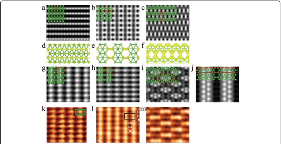
Figure 5 shows our simulated STM images for the free-standing and as-grown boron sheets on Ag(111) surface, as well as the partial charge density for the freestanding boron sheets. As shown in Fig. 5a, the freestanding buckled tri-angular boron sheet features stripes of bright spots. Figure
Fig. 3Calculated band structures forabuckled triangular,bβ12, andcχ3boron sheets. The Fermi energy was set to zero. The high-symmetry
[image:4.595.59.539.88.181.2] [image:4.595.59.538.615.705.2]5d indicates that the bright spots come from the pzorbit of
upper boron atoms. Figure 5b shows rows of dark round spots surrounded by bright hexagons. Obviously, the hex-agonal vacancies inβ12lattice shown in Fig. 1b result in the
dark spots, while the bright hexagons correspond to the σ orbits of boron atoms around the hexagon holes as shown in Fig. 5e. As shown in Fig. 5c, theχ3sheet displays
rhombo-hedra pattern of bright spots in dumbbell shape. These bright dumbbell spots actually are the pzorbits of the two
boron atoms and theσorbits formed between them. The boron sheets on the Ag substrate all have larger unit patterns relative to the freestanding ones because of the
mismatches between the unit cells of borophene and Ag(111) surface. Figure 5g shows our simulated STM image for buckled triangular boron sheet on Ag(111) surface. It displays stripes of bright spots in spindle shape, which agree very well with experimental observations [22]. Comparing with the image of freestanding buckled triangular boron sheet shown in Fig. 5a, the unit cell of STM image of buck-led triangular boron sheet on the Ag(111) surface increases to three times. And the shape changes to spindle from round. The STM image of β12 sheet on Ag(111) surface
shown in Fig. 5h shows rows of dark oval spots surrounded by four bright spots on its four corners. Different from the
Fig. 4Top and side views of boron sheets on Ag(111) surface.aBuckled triangular,bβ12,cχ3, anddχ3’boron sheet. The green and gray balls
represent boron and silver atoms, respectively. The rectangles and rhombus enclosed by solid black lines denote the unit cells of boron sheets on the Ag(111) surface
Fig. 5Simulated STM images of freestanding and epitaxial boron sheets on Ag(111) surface. Freestandingatriangular,bβ12, andcχ3boron
sheets. Partial charge density of freestandingdtriangular,eβ12, andfχ3boron sheets.gBuckled triangular,hβ12,iχ3, andjχ3’boron sheet on
[image:5.595.60.539.88.220.2] [image:5.595.56.540.427.675.2]the stripe phase for 2D boron sheets on the Ag(111) sur-face based on their STM observations, and both the STM images feature parallel rows of protrusions. How-ever, the shape of the bright spots in the two experimen-tal observations is different; they are spindle in Mannix et al.’s report [22] and oval in Feng et al.’s [23]. Our sim-ulated STM images of buckled triangular andβ12boron
sheets match very well with the experimental observed stripe phases in Ref. [22] and Ref. [23], respectively, and the images shown in Fig. 5g, h clearly reproduce the dif-ference between the experimental observations of Man-nix et al. [22] and Feng et al. [23]. It also provides us a way to distinguish the two lattice of buckled triangular and β12. As for the STM image of χ3 sheet on the
Ag(111) surface, as shown in Fig. 5i, it agrees with the experimental observation [23], but our result indicates
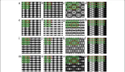
lated STM images show the light and dark stripes, which matches well with experiment result [22]. On the other hand, the simulated STM images of β12 borophene
maintain the oval shape at both the positive and negative bias voltage. Hence, buckled triangular structure is more likely to be the correct configuration of stripe phase. As for the STM image ofχ3borophene, Fig. 6 indicates that
the bright spots in all the images come from the boron atoms at the edge of hexagonal vacancies, but their bright contrast changes as the voltage changes from positive to negative. As the bias voltage of 0.2 and − 0.4 V, the brightness of the spots are similar. Addition-ally, our simulated STM images for the χ3’configuration
look similar at bias voltage from 0.8 to −1.0 V (Fig. 6). They all show the bright spots coming from the boron atoms on the edge of hexagonal vacancies, but only the
Fig. 6Simulated STM images for boron sheets on Ag(111). Buckled triangular borophene on Ag(111) ata0.8,e0.2,i−0.4, andm−1.0 V.β12
[image:6.595.56.539.408.684.2]higher boron atoms are visible and the lower boron atoms in the middle of the unit cell are invisible.
Conclusions
In summary, we performed first-principles calculations on the atomic structure, stability, and electronic prop-erty for the three 2D boron sheets which were grown on the metal surface very recently, namely, buckled triangu-lar, β12, andχ3lattice. Our calculations indicate that all
the three boron sheets are thermodynamically unstable without the support of metal substrate. The band struc-tures indicate that the buckled triangular boron sheet behaves as a metal with strong anisotropy and β12 and
χ3 boron sheets are also metallic without energy gaps.
Additionally, our results show that the energies for the three types of lattices are very close and the lattice match between the buckled triangular and β12 boron
sheets and Ag(111) surface is quite small. Furthermore, we have found that both buckled triangular and β12
boron sheets on the Ag(111) form the rectangular lattice and the parallel striped patterns of STM image but with little difference. Our results provide details to distinguish the two lattices. Most importantly, our simulated STM images give a new explanation to the experimentally ob-served boron sheets on the Ag(111) surface.
Abbreviations
2D:Two-dimensional; 3D: Three-dimensional; STM: Scanning tunneling microscopy
Acknowledgements
This work was supported by the National Natural Science Foundation of China (NNSFC) (21273172) and the program for New Century Excellent Talents in University (NCET-13-0471). This work was also supported by the 111 Project (B08040) and the Fundamental Research Funds for the Central Universities (3102015BJ(II)JGZ005, 3102015BJ023) in China. The supports from the University of Science and Technology Beijing and the University of Electronic Science and Technology China are appreciated.
Authors’Contributions
ZFL designed the study and performed the research. ZFL and XLF led the data discussion and interpretation. The manuscript was drafted by ZFL and XLF but was read and approved by all authors. YRA participated in performing research and helped to draft the manuscript. All authors read and approved the final manuscript.
Competing Interests
The authors declare that they have no competing interests.
Publisher’s Note
Springer Nature remains neutral with regard to jurisdictional claims in published maps and institutional affiliations.
Received: 12 May 2017 Accepted: 20 August 2017
References
1. Novoselov KS, Fal'ko VI, Colombo L, Gellert PR, Schwab MG, Kim K (2012) A roadmap for graphene. Nature 490:192–200
2. Xu M, Liang T, Shi MM, Chen HZ (2013) Graphene-like two-dimensional materials. Chem Rev 113:3766–3798
3. Balendhran S, Walia S, Nili H, Sriram S, Bhaskaran M (2015) Graphene analogues: elemental analogues of graphene: silicene, germanene, stanene, and phosphorene. Small 11:640–652
4. Ferrari AC, Bonaccorso F, Fal’Ko V, Novoselov KS, Roche S, Bøggild P, Borini S, Koppens FHL, Palermo V, Pugno N (2015) Science and technology roadmap for graphene, related two-dimensional crystals, and hybrid systems. Nano 7:4598
5. Johari P, Shenoy VB (2012) Tuning the electronic properties of semiconducting transition metal dichalcogenides by applying mechanical strains. ACS Nano 6:5449–5456
6. Klinovaja J, Loss D (2013) Spintronics in MoS2monolayer quantum wires.
Phys Rev B 88:4049–4057
7. Xu Y, Gan ZX, Zhang SC (2014) Enhanced thermoelectric performance and anomalous seebeck effects in topological insulators. Phys Rev Lett 112:770–777 8. Kunstmann J, Quandt A (2006) Broad boron sheets and boron nanotubes:
an ab initio study of structural, electronic, and mechanical properties. Phys Rev B 74:035413
9. Tang H, Ismailbeigi S (2007) Novel precursors for boron nanotubes: the competition of two-center and three-center bonding. Phys Rev Lett 99: 115501
10. Tang H, Ismailbeigi S (2009) Self-doping in boron sheets from first principles: a route to structural design of metal boride nanostructures. Phys Rev B Condens Matter 80:134113
11. Li WL, Zhao YF, Hu HS, Li J, Wang LS (2014) [B30]−: a quasiplanar chiral
boron cluster. Angew Chem 126:5646–5651
12. Zhou XF, Dong X, Oganov AR, Zhu Q, Tian Y, Wang HT (2014) Semimetallic two-dimensional boron allotrope with massless Dirac fermions. Phys Rev Lett 112:085502
13. Li WL, Chen Q, Tian WJ, Bai H, Zhao YF, Hu HS, Li J, Zhai HJ, Li SD, Wang LS (2014) The B35cluster with a double-hexagonal vacancy: a new and more
flexible structural motif for borophene. J Am Chem Soc 136:12257–12260 14. Piazza ZA, Hu HS, Li WL, Zhao YF, Li J, Wang LS (2014) Planar hexagonal B36
as a potential basis for extended single-atom layer boron sheets. Nat Commun 5:3113
15. Penev ES, Bhowmick S, Sadrzadeh A, Yakobson BI (2012) Polymorphism of two-dimensional boron. Nano Lett 12:2441–2445
16. Wu XJ, Dai J, Zhao Y, Zhuo ZW, Yang JL, Zeng XC (2012) Two-dimensional boron monolayer sheets. ACS Nano 6:7443–7453
17. Zhou XF, Artem RO, Wang ZH, Ivan AP, Alexander IB, Wang HT (2016) Two-dimensional magnetic boron. Phys Rev B 93:085406
18. Tang H, Ismailbeigi S (2010) First-principles study of boron sheets and nanotubes. Phys Rev B 82:115412
19. Özdoğan C, Mukhopadhyay S, Hayami W, Guvenc ZB, Pandey R, Boustani I (2010) The unusually stable B100fullerene, structural transitions in boron
nanostructures, and a comparative study ofα- andγ-boron and sheets. J Phys Chem C 114:4362–4375
20. Boustani I, Quandt A, Hernandez E, Rubio A (1999) New boron based nanostructured materials. J Chem Phys 110:3176
21. Evans MH, Joannopoulos JD, Pantelides ST (2005) Electronic and mechanical properties of planar and tubular boron structures. Phys Rev B 72:045434 22. Mannix AJ, Zhou XF, Kiraly B, Wood JD, Alducin D, Myers BD, Liu X, Fisher
BL, Santiago U, Guest JR, Yacaman MJ, Ponce A, Oganov AR, Hersam MC, Guisinger NP (2015) Synthesis of borophenes: anisotropic, two-dimensional boron polymorph. Science 350:1513
23. Feng B, Zhang J, Zhong Q, Li W, Li S, Li H, Cheng P, Meng S, Chen L, Wu K (2016) Experimental realization of two-dimensional boron sheets. Nat Chem 8:563
24. Liu YY, Penev ES, Yakobson BI (2013) Probing synthesis of two-dimensional boron by first-principles computations. Angew Chem Int Edit 52:3156–3159 25. Liu HS, Gao JF, Zhao JJ (2013) From boron cluster to two-dimensional
boron sheet on Cu(111) surface: growth mechanism and hole formation. Sci Rep 3:3238
26. Sun H, Li Q, Wan XG (2016) First-principles study of thermal properties of borophene. Phys Chem Chem Phys 18:14927–14932
27. Gao M, Li QZ, Yan XW, Wang J (2017) Prediction of phonon-mediated superconductivity in borophene. Phys Rev B 95:024505
28. Penev ES, Kutana A, Yakobson BI (2016) Can two-dimensional boron superconduct. Nano Lett 16:2522–2526
36. Wang H, Li Q, Gao Y, Miao F, Zhou XF, Wan XG (2016) Strain effects on borophene: ideal strength, negative Poisson’s ratio and phonon instability. New J Phys 18:073016