N A N O E X P R E S S
Open Access
Comparative Study of Photoelectric
Properties of Metamorphic InAs/InGaAs and
InAs/GaAs Quantum Dot Structures
Sergii Golovynskyi
1,2, Luca Seravalli
3, Oleksandr Datsenko
4, Giovanna Trevisi
3, Paola Frigeri
3, Enos Gombia
3,
Iuliia Golovynska
1, Serhiy V. Kondratenko
4, Junle Qu
1and Tymish Y. Ohulchanskyy
1*Abstract
Optical and photoelectric properties of metamorphic InAs/InGaAs and conventional pseudomorphic InAs/GaAs quantum dot (QD) structures were studied. We used two different electrical contact configurations that allowed us to have the current flow (i) only through QDs and embedding layers and (ii) through all the structure, including the GaAs substrate (wafer). Different optical transitions between states of QDs, wetting layers, GaAs or InGaAs buffers, and defect-related centers were studied by means of photovoltage (PV), photoconductivity (PC), photoluminescence (PL), and absorption spectroscopies. It was shown that the use of the InGaAs buffer spectrally shifted the maximum of the QD PL band to 1.3μm (telecommunication range) without a decrease in the yield. Photosensitivity for the metamorphic QDs was found to be higher than that in GaAs buffer while the photoresponses for both metamorphic and pseudomorphic buffer layers were similar. The mechanisms of PV and PC were discussed for both structures. The dissimilarities in properties of the studied structures are explained in terms of the different design. A critical influence of the defects on the photoelectrical properties of both structures was observed in the spectral range from 0.68 to 1. 0 eV for contact configuration (ii), i.e., in the case of electrically active GaAs wafer. No effect of such defects on the photoelectric spectra was found for configuration (i), when the structures were contacted to the top and bottom buffers; only a 0.83 eV feature was observed in the photocurrent spectrum of pseudomorphic structure and interpreted to be related to defects close to InAs/GaAs QDs.
Keywords:Nanostructure, Quantum dot, Metamorphic, InAs/InGaAs, Photoconductivity, Photoluminescence, Photovoltage, Absorption, Defects, Photoelectric
Background
InAs/InGaAs metamorphic semiconductor quantum dots (QDs) are interesting nanostructures that allow to have emission in the 1.3 and 1.55 μm ranges from
GaAs-based nanostructures [1–3]. InAs QDs
embed-ded in InGaAs matrix provide specific features, such as lattice mismatch and band discontinuities between the QDs and confining layers, which can be very useful for an adroit engineering of properties. In particular, the growth of InAs on the InGaAs metamorphic buffers (MB)
allows for reduction in the strain accumulated in QDs and, hence, modification of the energy of QD levels [4–7].
Recently, single photon emission at 1.3 μm from the metamorphic QDs has been demonstrated [8, 9], along-side the feasibility of photon emission evolution at such crucial wavelength and the perspective of a further extension of wavelength of emitted quantum light up to 1.55 μm [10]. Beside these very relevant results for quantum science applications, such nanostructures have been used for other novel devices such as metamorphic QD lasers [11, 12] and metamorphic QD solar cells [13]. Furthermore, a new design based on the metamorphic QDs for Broadband SLEDs (SuperLuminescent Diodes), devices of great interest for medical imaging applica-tions, has been proposed. This design predicts a relevant increase in the bandwidth of operation, even at * Correspondence:[email protected]
1College of Optoelectronic Engineering, Key Laboratory of Optoelectronic
Devices and Systems of Ministry of Education and Guangdong Province, Shenzhen University, 518060 Shenzhen, People’s Republic of China Full list of author information is available at the end of the article
wavelengths as long as 1.6 μm [14]. The emission efficiency of metamorphic InAs/InGaAs QDs has been demonstrated to be as high as the one of standard InAs/ GaAs QDs [4, 15]. Also, it was shown that InAs/InGaAs QDs were sensitive to normal incident light. This allows for the development of interband QD infrared photode-tectors operating at lower energies than well-known InAs/GaAs ones [16–18].
While considerable research on the morphological and optical properties of the InAs/InGaAs QD nanostruc-tures has been performed during last years [19–21], more work on the photoelectrical properties is still needed to provide a quantitative assessment of the role of strain-related defects in MBs and interfaces in device performances. A very relevant task is the suppression of the influence of the GaAs substrate and related inter-faces on device performance, as they might be highly filled by defect traps and non-radiative recombination levels as well as dopant centers [22, 23]. Deep-level tran-sient spectroscopy (DLTS) studies of InAs/In(Ga)As nanostructures [24, 25] give the major information on the defect level location within the bandgap, while the less-studied photoelectrical properties of the defects can be well determined by deep-level thermally stimulated conductivity (TSC) and photoconductivity (PC) spec-troscopy at direct current [26–30]. PC studies give infor-mation about the defects as well as the transitions involving QDs, wetting layer (WL), InGaAs buffers and substrate, carrier transport, and other mechanisms of nonequilibrium processes [27], examining comprehen-sively the photoelectrical properties of the structure.
In a previous publication [30], we have carried out an in-depth study of a single metamorphic QD structure grown by molecular beam epitaxy (MBE) on semi-insulating (si)-GaAs substrates. We focused on the com-plex quantum-level system, composed by the QDs, WL, InGaAs embedding layer, and n-doped MB. It has been shown that the metamorphic QDs absorb and emit in the 1.3-μm range at room temperature (RT), while main-taining an efficient emission. The vertical configuration, used for photoelectrical characterization, consisted of two contacts deposited to MBE grown buffer layers that allowed to avoid the flow of electrical current through the n-InGaAs/n-GaAs and n-GaAs/substrate interfaces. We showed that by depositing a thick InGaAs MB on the substrate, we have achieved a strong suppression of the impact of the interface on the electrically active layers. While considerable advances in the understanding of the structure peculiarities were reached, a definitive assessment of the structure properties in comparison with the conventional InAs/GaAs QDs was not possible.
In this work, we compared the photoelectric proper-ties of the metamorphic InAs/InGaAs QD structure with those of a standard InAs/GaAs QD one. The GaAs
structure has been designed in order to have a direct com-parison with the metamorphic one, providing a reference to ascertain the role of the metamorphic InGaAs layer on photoelectric properties. This allows to compare QD emission and photosensitivity from the two structures be-cause of the less number of influencing parameters. The photoelectrical measurements are carried out at vertical configurations for electrical contacts: (i) to the MBE layers to characterize only QDs and embedding layers and (ii) to the top and substrate of the samples in order to evaluate the effect of GaAs/InGaAs and substrate/n-GaAs inter-faces on the carrier photogeneration and transport.
Methods
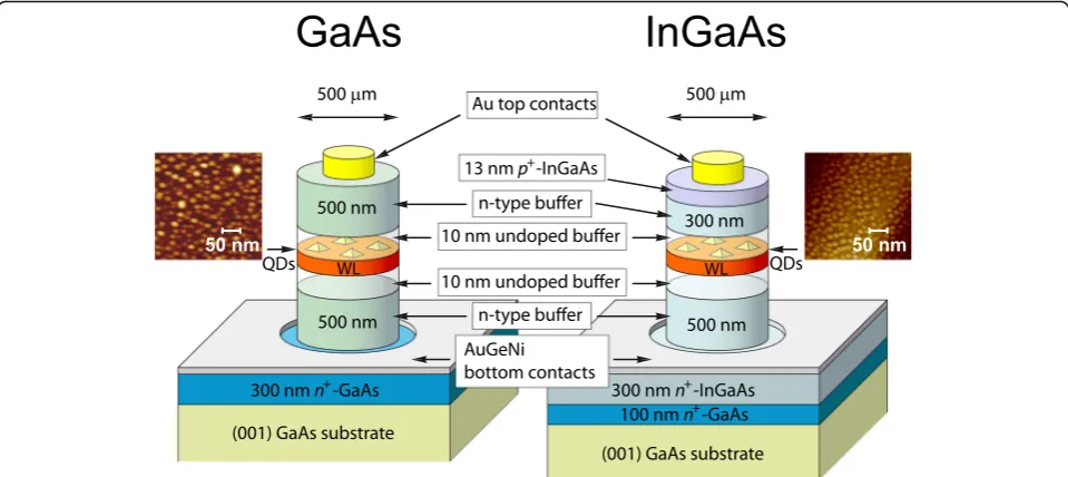
The structures were prepared by MBE on (001) si-GaAs substrates. Substrates were provided by Wafer Technology that specified them to ben-type, with values of 3 × 107cm −3
carrier concentration, thickness of 500μm, and a resist-ivity of 2 × 10⁷Ωcm. The metamorphic InAs/InGaAs QD structure consists of (i) 0.1 μm n+-GaAs buffer layer grown at 600 °C, (ii) 300 nm thickn+-doped In0.15Ga0.85As
MB with n= 5 × 1018 cm−3 grown at 490 °C, (iii)
500 nm thick n-doped In0.15Ga0.85As MB with n= 3 × 1016 cm−3grown at 490 °C, (iv) 3.0 monolayers of self-assembled InAs QDs on a WL grown by atomic layer MBE (ALMBE) at 460 °C embedded in the middle of a 20 nm undoped In0.15Ga0.85As layer, (v) 300 nm n-doped In0.15Ga0.85As upper capping layer withn= 3 × 1016cm−3 grown at 490 °C, and (vi) 13 nmp+-doped In0.15Ga0.85As cap withp= 2 × 1018cm−3grown at 490 °C (Fig. 1) [4, 15]. As discussed in Ref. [30], undoped layers were used to separate QDs from n-doped regions to reduce the effect of non-radiative recombination centers, thus maximizing the QD light emission efficiency.
The InAs/GaAs QD structure consists of (i) 0.3 μm
n+-GaAs buffer layer with n= 5 × 10¹⁸
cm−3 grown at 600 °C, (ii) 500 nm thick n-doped GaAs MB with n= 3 × 1016 cm−3 grown at 600 °C, (iii) 3.0 monolayers of InAs QDs grown by ALMBE at 460 °C embedded in
a 20 nm undoped GaAs layer, and (iv) 500 nm n
-doped GaAs upper capping layer with n= 3 × 1016 cm −3
grown at 600 °C (Fig. 1). Atomic force microscopy (AFM) images of the uncapped structures are shown in Fig. 1. Previous analysis of AFM data provided QD
densities of 1 × 1011 cm-2 and QD dimensions of
20 nm for base diameters and 4.9 nm for heights for metamorphic QDs [4, 31]. For standard QDs, surface densities are 2 × 1011 cm−2, base diameters are 21 nm, and heights are 5.0 nm [4, 32].
As shown in the Fig. 1, the vertical (in the growth dir-ection) electrical contacts were made by defining circu-lar mesas with 500 μm diameter and by etching of the
n-InGaAs andn-GaAs buffers down ton+-layer in a so-lution of C6H8O7:H2O:H2O2 (5:5:1) at 20 °C. Ohmic
contacts were obtained by evaporating and annealing (at 400 °C for 1 min in nitrogen atmosphere) the Au0.83Ge0.12Ni0.05 alloy [33, 34] on the bottom n +
-InGaAs andn+-GaAs layers, respectively. Au top con-tacts were then evaporated with a diameter of 400 μm and a thickness of 70 nm. Thick indium contacts were also soldered on the substrate bottoms of other pieces of same samples and annealed at 400 °C, in order to have measurements also with current flowing through
the GaAs buffer and si-GaAs substrate. Wires were
soldered to the contact layers of all four samples and connected to sample holder pins. It should be noted that the contacts of indium with si- and n-GaAs sub-strates are generally reported to be ohmic, not Schottky [35–37]. We have verified this by the IV measurements of the In-GaAs contacts; the current-voltage character-istics were found to be linear (data not shown).
The thinp+-InGaAs layer between the Au contact and then-InGaAs layer is used to enhance the barrier height since the structure obtained by the simple deposition of a metal on n-InGaAs exhibits a relatively low Schottky barrier height, following the approach proposed in Ref. [38] and already used in other works [39, 40]. An extended analysis of the electrical characteristics of metal/p+-cap/InGaAs/InP structures is reported in Ref. [41], where the band bending profile of the structure is also shown. So the deposition of thin p+-InGaAs layer provides approximate similarity of Schottky barrier height of top Au contact maintaining resemblance of barrier profile for both metamorphic and InAs/GaAs structures.
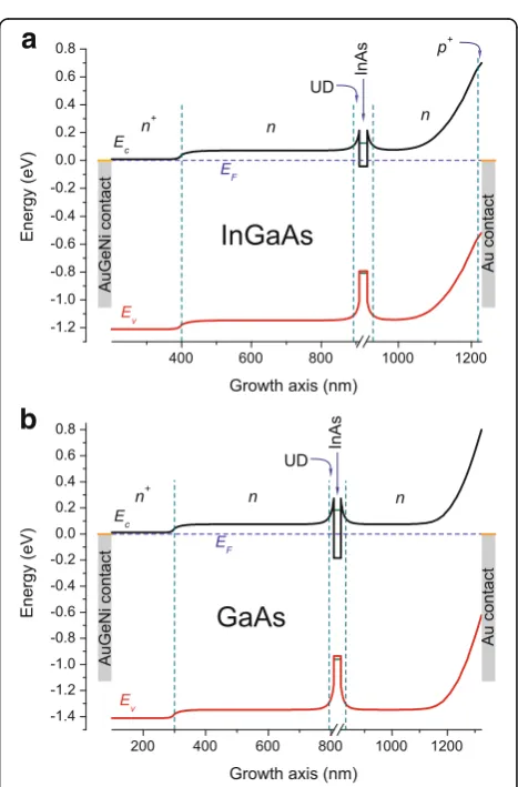
For structure and contact designing as well as under-standing of the energy profile for both structures composed by the InGaAs or GaAs MBs, In(Ga)As QDs, undoped cap layer, and Au/AuGeNi contacts, the calcu-lations were carried out using Tibercad software [42]. Band profiles were modeled in the drift-diffusion approximation, taking in consideration strain conditions, densities of traps related to defects at the InGaAs/GaAs interface region, depletion layers near contacts, and appropriate Schottky barriers heights. Calculating QD band offsets the data from AFM and photoluminescence (PL) measurements were utilized; the simulations were performed, considering experimentally obtained ground state transition energy (see the “Results”section), height and lateral width of QDs, and a low content of Ga in InAs QDs. However, the theoretical study of QDs is out of scope of this paper, and QD modeling has been performed only for representation of whole heterostruc-ture band profiles between contacts.
The PL characterization was performed by exciting the sample with a laser light at 532 nm with power densities
of 5 W/cm2 at 10 and 300 K; emission spectra were
measured by a fast Fourier transform spectrometer with a cooled Ge detector.
Vertical photocurrent (photosensitivity) and photovol-tage (PV) spectra were measured using an infrared prism spectrometer in the 0.6 to 1.8 eV range using normal incidence excitation geometry at RT (300 K) and were normalized by the intensity of light source. The photo-current was measured using a photo-current amplifier and direct current technique, with a bias voltage between 0
[image:3.595.58.538.88.302.2]and −4 V. The current was measured with a Picotest M3511A multimeter as a voltage signal drop across a series load resistance of 1 kΩ (see the inset in Fig. 5): such signal was orders of magnitudes lower than the voltage drop across the sample. The current-voltage characteristics were measured in the dark and under illumination with intensity of 1.5 mW/cm2 at RT. The absorption spectrum was measured using the diffraction spectrophotometer in the same energy range at RT. The onsets of spectral bands were estimated by applying standard methods based on the differentiation of the spectra which allow to find different critical points [43].
Results
A. Photoluminescence
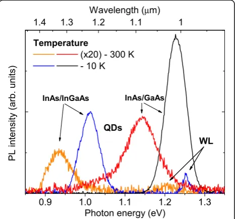
The PL spectra at both 10 and 300 K of the InAs QD embedded in the In0.15Ga0.85As MB
and conventional InAs/GaAs QDs grown on si -GaAs substrates are presented in Fig. 2. The emission spectrum of the metamorphic QD structure at 10 K shows two bands at 1.02 (QDs) and 1.26 eV (WL), that redshift at RT to 0.94 and 1.20 eV, respectively, while InAs/GaAs QDs emit at 1.23 eV at 10 K and 1.15 at RT. It should be noted that the metamorphic QDs emit in the telecom range at 1.3 μm at RT as it have been described in earlier papers, while
maintaining an efficient emission that is about only half of the emission intensity of InAs/GaAs QDs [4, 10, 15].
B. Absorption
Room temperature absorption spectra of the InAs/ In0.15Ga0.85As and InAs/GaAs QD structures are
presented in Fig.3. The features of the
metamorphic InAs/In0.15Ga0.85As QD structure
spectrum in Fig.3(a) have been identified elsewhere [30]. In particular, the threshold at 0.68 eV is related to the EL2 family defect centers [22–29]. The step at 0.85 eV is caused by the absorption in ensemble of the QDs, which corresponds to the onset of the QD peak in the PL spectrum at RT, whereas another one at 0.98 eV can be attributed to the transition from the first QD heavy hole excited state to the continuum of In0.15Ga0.85As MB
conduction band states. The feature at 1.11 eV can be caused by the transitions between band and shallow defect levels in the MB, and the one at 1.17 eV can be related to the WL absorption, which corresponds to the WL PL peak at RT. But the rise after 1.17 eV is so sharp that can rather be
attributed to the carrier generation in both the WL and In0.15Ga0.85As MB through shallow levels. The
calculation of the In0.15Ga0.85As MB bandgap,
considering the exact amount of strain for a thickness of 500 nm and the correct Varshni parameters, gives a value of 1.225 eV at 300 K [44]. Finally, the last step at 1.36 eV with the following plateau is obviously related to the absorption of the n-doped GaAs buffer layer, which might contain shallow levels, redshifting the interband absorption of the GaAs [24,25]. In Fig.3b, we show the absorption spectrum of the InAs/GaAs QD structure: the threshold of absorptance occurs at 0.68 eV, while a series of steps are observed at 1.05 and 1.3 eV, with the last step near 1.36 eV followed by plateau. The threshold and the last step occur at the same energies of the metamorphic structure allowing to attribute the first one to the EL2 family defect centers [22–29] and the 1.36 eV step to the GaAs buffer layers. The QD PL spectrum confirms the attribution of the 1.05-eV step to QD ground states, while the slight step at 1.3 eV can be attributed to the transitions in the WL [45]. C. Photovoltage and photocurrent
The PV spectra of both the InAs/In0.15Ga0.85As and
InAs/GaAs samples are also presented in Fig.3. All transitions mentioned above in the absorption data contribute to the PV signal. However, no signal from the EL2 centers is observed in the spectra of samples contacted to the thick InGaAs or GaAs buffers. On the other hand, in structures where current flows also through the substrate, the PV signal onset occurs at 0.68 and 0.72 eV, for metamorphic and conventional structures,
Fig. 2(Color online) Room temperature (T= 300 K) and 10 K PL spectra of the metamorphic InAs/In0.15Ga0.85As and conventional InAs/ GaAs QD structures. The RT spectra have been multiplied by 20
[image:4.595.58.291.477.694.2]respectively (inset in Fig.3). Additionally, the wide band peaked at 1.24 eV with edge at 1.11 eV is observed in the InAs/In0.15Ga0.85As sample PV
spectrum, with fewer steps in comparison with the absorption spectrum (Fig.3a). This PV spectrum feature points out at the correctness of assumption that after 1.11 eV, the carrier generation occurs mainly in the In0.15Ga0.85As MB including the way
through shallow levels.
In PV measurements, the optically excited charge carriers drift to different sides according to the band structure slope. The Au Schottky barrier height is 0.7 eV for InGaAs and 0.8 eV for GaAs, resulting in a rather steep slope of energy bands at the surface of the top buffers [33, 34]. The band schemes of studied structures are pictured in Fig. 4 based on calculations using Tibercad software, as described above. Hence, the electrons (holes) excited in the buffers move to the sample bottom (top), thus giving a positive potential at the structure surface and a negative one at the AuGeNi contact. The wide space charge area at the Schottky barrier, about 200 nm with 0.7–0.8 eV height, makes difficult for electrons to move from QDs to the surface, so, at the existing conditions, electrons excited in the QDs and WL move predomin-antly towards the substrate side as well giving the same PV sign as the buffer layer. The sharp fall of the PV signal from the metamorphic QD sample above 1.36 eV is caused by an effect of the GaAs layers which has been described elsewhere [30]. The slight fall of the PV signal from the InAs/GaAs sample resulting in the small feature after 1.36 eV can be explained by the absorption edge of the MBE grown upper GaAs buffer, overshading the QDs
Fig. 3(Color online) Room temperature (T= 300 K) PV and absorption spectra of theametamorphic InAs/In0.15Ga0.85As andbconventional InAs/GaAs QD structures. PV was measured contacted to only MBE layers; in theinset, the PV spectra measured through the semi-insulating GaAs substrates in the metamorphic and conventional QD structures (solid and dash line, respectively). The QD PL spectra in arbitrary units are shown for easier comparison
[image:5.595.58.538.89.288.2] [image:5.595.305.539.340.695.2]and WL being obviously the more efficient contributors to PV. Then, the subsequent band-to-band absorption above 1.4 eV in then-GaAs buffer leads to the sharp rise of PV.
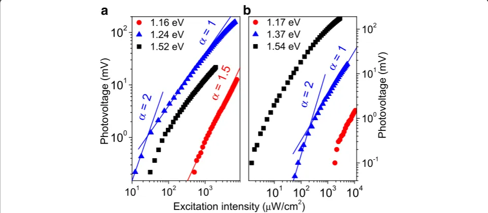
The dependences of PV on the excitation intensity (Iex) measured at characteristic points of the spectra are presented in Fig. 5. For the InAs/In0.15Ga0.85As sample (Fig. 5a), the point at 1.16 eV corresponds to the efficient absorption in the mentioned above shallow acceptors in the MB whereas the band-to-band absorption in the WL is too weak, 1.24 eV (spectrum peak) corresponds to the In0.15Ga0.85As band, while the value at 1.52 eV matches the plateau region. The near-surface absorption in the upper In0.15Ga0.85As MB predominantly occurs at so high energy; this can be concluded from the absorption spectrum. Indeed, according to absorptance data, only about 20% of light reach the GaAs layer at 1.36 eV. This part becomes certainly lower at higher energies.
The InAs/GaAs structure is studied at 1.17, 1.37, and 1.54 eV (Fig. 5b). The first point is in the range of efficient absorption in the QDs; the second one is the range where the transitions from the WL states are the most efficient whereas the absorption in then-GaAs layer has no substan-tial impact. At the point of 1.54 eV, the signal is mainly caused by the intrinsic absorption in the GaAs buffer.
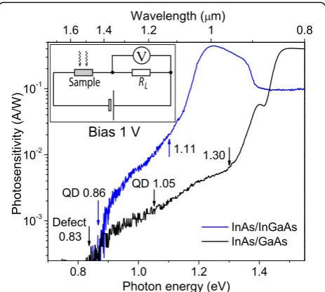
The photocurrent has been investigated at 1 V nega-tive bias (“−” at the top and“+” at the bottom contact). The measured spectra, presented in Fig. 6 as photosensi-tivity, show mainly the same structure features as the PV spectra considered above. The components of QDs, WL, and In0.15Ga0.85As or GaAs buffers as well as doped GaAs buffer layers manifest at the PC spectra at the same energies; however, the PC threshold of InAs/GaAs structure is observed at 0.83 eV that is much lower than
the QD state transitions. It should be noted that this value coincides with that obtained by DLTS measure-ments for similar InAs/GaAs QD structure [15, 46, 47]. Measuring the DLTS spectra at different distances from QDs, 0.84 eV traps have been observed in the QD plane. Such traps have been attributed to defects related to the presence of ripened QDs [46]. This allows to consider 0.83 eV level as the InAs-QD/GaAs interface defect.
Discussion
In the present work, we have focused on the observation of photoelectric properties of the metamorphic InAs/ In0.15Ga0.85As QD nanostructures and conventional InAs/GaAs QD ones grown with similar design on thick buffers. The use of InxGa1−xAs MB and embedding layers successfully shifts the QD optical transition ener-gies to lower ones [4, 9, 15, 30], by reducing the QD strain [3–7]; as a side effect, MB-related defects are present in the InGaAs material. It should also be consid-ered that a significant impact on the carrier transport and its lifetime may be caused by the formation of spe-cific band bending at InGaAs/GaAs and InAs/InGaAs interfaces. Such features determine the properties of samples leading to differences not only in emission ener-gies but also in PL emission intensity, photosensitivity, carrier leakage through defects, and other.
The PL characterization of the InAs QD-capped struc-tures embedded in the In0.15Ga0.85As MB in comparison with the InAs QDs grown on GaAs has shown an effi-cient QD emission that is about a half of the emission of the InAs/GaAs QDs, known to be very efficient light sources [48, 49], at both 10 and 300 K (Fig. 2). At RT, the metamorphic QDs emit at 0.94 eV, while the InAs/
Fig. 5(Color online) Dependences of PV on the excitation intensity at different photon energies foraInAs/In0.15Ga0.85As andbInAs/GaAs structures; thelinesare the functionsf(Iex)∝(Iex)α
[image:6.595.57.538.494.704.2]GaAs ones emit at 1.15 eV. Considering that QD density of InAs/GaAs standard QDs is double that of meta-morphic QDs [4], we can roughly estimate the efficien-cies per one QD to be similar for both the samples. This evidences that the presence of the inherent InGaAs dislocations and defect levels do not severely impact the optical quality of the QD cladding layers [50].
It can be noticed that the investigated metamorphic QDs emit in the telecom range at 1.3 μm at RT, while maintaining a good PL efficiency that has been described in earlier papers [4, 9, 15, 30]. The following features of metamorphic structures affect on such PL redshift: (i) at the identical growth parameters, the metamorphic QDs self-assemble in the larger size and with the higher QD density [4]; (ii) the reduction of QD-cladding layer discontinuities downshifts the confinement levels by values of 0.01–0.1 eV (based on the calculation by Ref. [51, 52]); and (iii) some shift of confinement levels is caused by the strain reduction [4, 5].
The absorption and photoelectric characterization data agree with the experimental PL transitions in both struc-tures. The spectra show the effective absorption of normal incident light in the QD, WL, and buffers (Fig. 3), overlap-ping in band positions with the PL data on the QD and WL transitions as taken from Fig. 2. All the transitions found in the absorption data contribute to the PV and PC signal.
Summing up the results, we can affirm that photoelec-tric properties are similar to the two types of structures. The QD components manifest in the photoelectric spec-tra as wide bands positioned at the same energies of PL
ones. The main differences are due to the In0.15Ga0.85As MB which causes the reduction of the QD optical transi-tion energies. On such structures, we still observe an effective detection of photocarriers coming from QDs. The photosensitivity spectra in Fig. 6 allow to quantita-tively compare the structures under investigation. Being comparable from buffers (near 0.4 A/W), the photo-sensitivity of the metamorphic InGaAs nanostructure is higher in the QD range, 4 × 10⁻⁴vs 2.7 × 10⁻⁴A/W. Con-sidering that QD density of InAs/GaAs standard QDs is double that of metamorphic QDs [4], it appears that PC excited in metamorphic QDs is a more efficient process. Taking into account that the PL efficiencies per one QD of both the structures are similar, one can conclude that an additional leakage of photogenerated carriers might occur in the InAs/GaAs sample by means of the non-radiative recombination through the interface levels like energy of conductivity band (Ec)—0.83 eV reported earlier [15, 47]
and found by PC. It is noteworthy that a more comprehen-sive comparison is possible in PC, as the generation and recombination of carriers are involved in the PC mechan-ism, along with their transport and loss through non-radiative recombination in buffer.
The level Ec—0.83 eV was not observed in the InAs/
In0.15Ga0.85As samples (Fig. 6): in previous works on DLTS, such a level was attributed to extended defects related to strain relaxation in the vicinity of QDs [46]. Hence, present results suggest that such levels might not be present in metamorphic structures, possibly due to the lower level of strain between InAs QDs and InGaAs layers, in comparison with the InAs/GaAs system.
On the other hand, an indirect evidence of some recombination center existence has been found in both the structures from the PV dependences on excitation intensity. All the PV dependences tend to be superlinear close to (Iex)2at lower intensities. Since such a depend-ence can be explained within a model of Shockley-Read recombination of free carriers through two types of centers [48, 49], this could indicate the presence of defects in both GaAs and InGaAs buffers. For higher excitation intensities, the defect states are saturated, and henceforth, the curves, except at 1.16 eV for meta-morphic sample, have a linear part in the middle which transforms to sublinear for the highest intensities. Such a behavior might be explained by direct recombination of the nonequilibrium carriers in a doped semicon-ductor, considering simple rate equations [53, 54]. In contrast, the dependence at 1.16 eV of the metamorphic sample in Fig. 5a is close to (Iex)3/2. This shape also implies recombination of carriers excited band-to-band, i.e., within QDs, through at least two recombination levels [50]. We think this process occurs through shal-low levels, possibly related to defects located in MBE grown buffers and strained interfaces that account for
[image:7.595.58.290.87.295.2]the 1.11 eV sharp feature in the absorption and PV spec-tral curves. Those defects are commonly observed by means of DLTS [15, 24, 25] and TSC [26, 27, 29] measurements.
As for EL2 defect levels in buffer layers located near 0.75 eV below the conduction band [22–25], no signal from these centers is observed in the spectra of samples with the contacts on the thick InGaAs or GaAs MBE buffers, while measuring PV through the substrate, the signal onset occurs at 0.68 and 0.72 eV for metamorphic and standard structures, respectively (inset in Fig. 3). As well the onset of both the absorption spectra at 0.68 eV, we attribute to the transition from EL2 defect center to the conduction band considering the possible way through the shallow defect levels [24–27, 29]. Similar redshift of EL2-related bands in optical transition have been described for InGaAs/GaAs nanostructures [27, 30]. However, the fact that no signal below QD spectral band is observed in the PV spectra from only MBE layers means a low amount of EL2-like non-radiative recombination centers in the metamorphic and GaAs buffers overall, providing the effective detection of photocarriers coming from even a single layer of QDs, whereas the high density of recombination centers in the GaAs substrates and
n+
-GaAs layers of the structures under investigation has been confirmed by the PV characterization of samples measured through the substrate (inset in Fig. 3).
Hence, by studying samples with different contact con-figuration (only on MBE layers or on the bottom part of the substrate), we were able to conclude that the regions with higher defect density are the GaAs substrate and GaAs buffer layers [15, 22, 23, 55, 56]. Henceforth, the InGaAs/GaAs interface region did not show to have a strong influence on the electrical properties of the QD structures.
Conclusions
We can conclude that the photovoltaic properties of both types of studied samples (i.e., metamorphic InAs/InGaAs and pseudomorphic InAs/GaAs QD structures) are mostly similar. An efficient detection of photocarriers has been shown for the sample with InGaAs MB, which is instru-mental to redshift the QD emission towards the telecom-munication range (1.3μm). A critical influence of the EL2 deep levels on the photoelectrical properties of both the structures was found when the current flowed through the substrate, while no such effect was observed in the PV spectra in the case of samples contacted to the MBE layers. However, the slight recombination of the photoex-cited carriers through non-radiative centers was observed in intensity-driven PV measurements of both samples. The latter contact geometry, along with the thick buffers on substrate, allowed for strong suppression of the influ-ence of photoactive deep levels in the interfaces and
si-GaAs substrate on the photoelectric properties of both structures. No relevant contribution of a level at
Ec—0.83 eV was observed in the metamorphic InAs/
InGaAs QD structures, in stark difference with the InAs/ GaAs ones. This result allows us to conclude that the metamorphic InAs/InGaAs heterostructures are not affected by levels related to extended defects in the vicinity of QD, apparently due to a lower strain in comparison with the InAs/GaAs structure. Based on the results on optical and electrical properties of metamorphic QDs presented here, it can be concluded that efficient photonic devices at 1.3 μm can be developed with similar nano-structures as an active material. This could be of great interest for the fabrication of GaAs-based photonic systems operating in the telecom range.
Abbreviations
AFM:Atomic force microscopy; ALMBE: Atomic layer molecular beam epitaxy; DLTS: Deep-level transient spectroscopy;Ec: Energy of conductivity band;Iex: Excitation intensity; MB: Metamorphic buffer; MBE: Molecular beam epitaxy; PC: Photoconductivity; PL: Photoluminescence; PV: Photovoltage; QD: Quantum dot; RT: Room temperature;si: Semi-insulating; TSC: Thermally stimulated conductivity; WL: Wetting layer
Acknowledgements
This work was supported in part by COST Action“Nanoscale Quantum Optics”of European Union and the National Basic Research Program of China (2015CB352005); the National Natural Science Foundation of China (61525503/61378091/61620106016); Guangdong Natural Science Foundation Innovation Team (2014A030312008); Hong Kong, Macao, and Taiwan cooperation innovation platform and major projects of international cooperation in Colleges and Universities in Guangdong Province (2015KGJHZ002); and Shenzhen Basic Research Project (848/000004022801, JCYJ20150930104948169, JCYJ20160328144746940,
GJHZ20160226202139185). The authors are also thankful for the AFM characterization, which has been carried out at CIM, University of Parma, Italy and for the help in alternative calculation of nanostructure using homemade software provided by Sergii Kurlov from Humboldt University.
Authors’Contributions
SG, LS, and OD proposed and guided the overall project. LS, GT, and PF designed and grew the samples, measured the luminescence spectra, performed the AFM microscopy and made the band profile calculations. EG and SG made the electrical contacts and technical part. SG, OD, and IG performed the PV, PC, and absorption measurements. SG, OD, and LS wrote the manuscript, with contributions from all authors. SVK, TYO, and JQ participated in the discussions and edited the manuscript. LS, TYO, and JQ provided managerial supports and supervised the research. All authors reviewed and approved the final manuscript.
Competing Interests
The authors declare that they have no competing interests.
Publisher’s Note
Springer Nature remains neutral with regard to jurisdictional claims in published maps and institutional affiliations.
Author details
1College of Optoelectronic Engineering, Key Laboratory of Optoelectronic
Devices and Systems of Ministry of Education and Guangdong Province, Shenzhen University, 518060 Shenzhen, People’s Republic of China.2Institute
of Semiconductor Physics, NAS of Ukraine, 45 Nauki Ave, 03028 Kyiv, Ukraine.
3Institute of Materials for Electronics and Magnetism, CNR-IMEM, Parco delle
Scienze 37a, I-43100 Parma, Italy.4Department of Physics, Taras Shevchenko
National University of Kyiv, 64 Volodymyrska St, 01601 Kyiv, Ukraine.
Received: 10 January 2017 Accepted: 20 April 2017
References
1. Balakrishnan G, Huang S, Rotter TJ, Stintz A, Dawson LR, Malloy KJ, Xu H, Huffaker DL (2004) 2.0μm wavelength InAs quantum dashes grown on a GaAs substrate using a metamorphic buffer layer. Appl Phys Lett 84:2058 2. Semenova ES, Zhukov AE, Mikhrin S, Egorov AY, Odnoblyudov VA, Vasilev AP, Nikitina EV, Kovsh AR, Kryzhanovskaya NV, Gladyschev AY, Blokhin SA, Musikhin YG, Maksimov MV, Shernyakov YM, Ustinov VM, Ledentsov NN (2004) Metamorphic growth for application in long-wavelength (1.3–1.55μm) lasers and MODFET-type structures on GaAs substrates. Nanotechnology 15:S283 3. Seravalli L, Minelli M, Frigeri P, Allegri P, Avanzini V, Franchi S (2003) The
effect of strain on tuning of light emission energy of InAs/InGaAs quantum-dot nanostructures. Appl Phys Lett 82:2341
4. Seravalli L, Frigeri P, Nasi L, Trevisi G, Bocchi C (2010) Metamorphic quantum dots: quite different nanostructures. J Appl Phys 108:064324 5. Wang P, Chen Q, Wu X, Cao C, Wang S, Gong Q (2016) Detailed study of
the influence of InGaAs matrix on the strain reduction in the InAs dot-in-well structure. Nanoscale Res Lett 11:119
6. Maximov MV, Kryzhanovskaya NV, Nadtochiy AM, Moiseev EI, Shostak II, Bogdanov AA, Sadrieva ZF, Zhukov AE, Lipovskii AA, Karpov DV, Laukkanen J, Tom J (2014) Ultrasmall microdisk and microring lasers based on InAs/ InGaAs/GaAs quantum dots. Nanoscale Res Lett 9:657
7. Zhou X, Chen Y, Xu B (2011) Optical identification of electronic state levels of an asymmetric InAs/InGaAs/GaAs dot-in-well structure. Nanoscale Res Lett 6:317
8. Munoz-Matutano G, Barrera D, Fernandez-Pousa CR, Chulia-Jordan R, Seravalli L, Trevisi G, Frigeri P, Sales S, Martinez-Pastor J (2016) All-Optical Fiber Hanbury Brown & Twiss Interferometer to study 1300 nm single photon emission of a metamorphic InAs quantum dot. Sci Rep 6:27214 9. Seravalli L, Trevisi G, Frigeri P, Rivas D, Munoz-Matutano G, Suarez I, Alen B,
Canet J, Martinez-Pastor JP (2011) Single quantum dot emission at telecom wavelengths from metamorphic InAs/InGaAs nanostructures grown on GaAs substrates. Appl Phys Lett 98:173112
10. Seravalli L, Trevisi G, Frigeri P (2012) Design and growth of metamorphic InAs/InGaAs quantum dots for single photon emission in the telecom window. CrystEngComm 14:6833
11. Xin Y, Vaughn L, Dawson LR, Stintz A, Lin Y, Lester LF, Huffaker DL (2003) InAs quantum-dot GaAs-based lasers grown on AlGaAsSb metamorphic buffers. J Appl Phys 94:2133
12. Mi Z, Bhattacharya P (2008) Pseudomorphic and metamorphic quantum dot heterostructures for long-wavelength lasers on GaAs and Si. IEEE J Sel Top Quant 14:1171
13. Gandhi JS, Kim CU, and Kirk WP. Enhanced Voc in InAs quantum-dot based
p-i-nsolar cells using a non-alternating strain-balancing epitaxial growth method. Conference Record of the 38thIEEE Photovoltaic Specialists Conference. 2012:789.
14. Seravalli L, Gioannini M, Cappelluti F, Sacconi F, Trevisi G, Frigeri P (2016) Broadband light sources based on InAs/InGaAs metamorphic quantum dots. J Appl Phys 119:143102
15. Trevisi G, Seravalli L, Frigeri P, Prezioso M, Rimada J, Gombia E, Mosca R, Nasi L, Bocchi C, Franchi S (2009) The effects of quantum dot coverage in InAs/(In)GaAs nanostructures for long wavelength emission. Microelectron J 40:465
16. Lu X, Vaillancourt J, Meisner MJ, Stintz A (2007) Long wave infrared InAs-InGaAs quantum-dot infrared photodetector with high operating temperature over 170 K. J Phys D Appl Phys 40:5878
17. Lu X, Meisner MJ, Vaillancourt J, Li J, Liu W, Qian X, Goodhue WD (2007) Modulation-doped InAs-InGaAs quantum dot longwave infrared photodetector with high quantum efficiency. Electron Lett 43:1 18. Kim JO, Sengupta S, Barve AV, Sharma YD, Adhikary S, Lee SJ, Noh SK,
Allen MS, Allen JW, Chakrabarti S, Krishna S (2013) Multi-stack InAs/ InGaAs sub-monolayer quantum dots infrared photodetectors. Appl Phys Lett 102:011131
19. Kettler T, Karachinskii LY, Ledentsov NN, Shchukin VA, Fiol G, Kuntz M, Lochmann A, Schulz O, Reissmann L, Posilovic K, Bimberg D, Novikov SV, Shernyakov YM, Gordeev NY, Maksimov MV, Kryzhanovskaya NV, Zhukov AE, Semenova ES, Vasil’ev AP, Ustinov VM, Kovsh AR (2006) Degradation-robust single mode continuous wave operation of 1.46μm metamorphic quantum dot lasers on GaAs substrate. Appl Phys Lett 89:041113
20. Seravalli L, Trevisi G, Frigeri P, Royce RJ, Mowbray DJ (2012) Energy states and carrier transport processes in metamorphic InAs quantum dots. J Appl Phys 112:034309
21. Ghanad-Tavakoli S, Naser MA, Thompson DA, Deen MJ (2009) Experimental characterization and theoretical modeling of the strain effect on the evolution and interband transitions of InAs quantum dots grown on InxGa1−xAs (0.0⩽x⩽0.3) metamorphic pseudosubstrates on GaAs
wafers. J Appl Phys 106:063533
22. Kaminska M (1988) Optical properties of EL2. Rev Phys Appl 23:793 23. Kaminska M, Skawronski M, Lagowski J, Parsey JM, Gatos HC (1983)
Intracenter transitions in the dominant deep level (EL2) in GaAs. Appl Phys Lett 43:302
24. Farrow RFC (1995) Molecular beam epitaxy: applications to key materials. Noyes, New Jersey
25. Asano T, Fang Z, Madhukar A (2010) Deep levels in GaAs(001)/InAs/InGaAs/ GaAs self-assembled quantum dot structures and their effect on quantum dot devices. J Appl Phys 107:073111
26. Vakulenko OV, Golovynskyi SL, Kondratenko SV (2011) Effect of carries capture by deep levels on lateral photoconductivity of InGaAs/GaAs quantum dot structures. J Appl Phys 110:043717
27. Golovynskyi SL, Dacenko OI, Kondratenko SV, Lavoryk SR, Mazur YI, Wang ZM, Ware ME, Tarasov GG, Salamo GJ (2016) Intensity-dependent nonlinearity of the lateral photoconductivity in InGaAs/GaAs dot-chain structures. J Appl Phys 119:184303
28. Golovynskyi SL, Mazur YI, Wang ZM, Ware ME, Vakulenko OV, Tarasov GG, Salamo GJ (2014) Excitation intensity dependence of lateral photocurrent in InGaAs/GaAs dot-chain structures. Phys Lett A 378:2622
29. Kondratenko SV, Vakulenko OV, Mazur YI, Dorogan VG, Marega E Jr, Benamara M, Ware ME, Salamo GJ (2014) Deep level centers and their role in photoconductivity transients of InGaAs/GaAs quantum dot chains. J Appl Phys 116:193707
30. Golovynskyi SL, Seravalli L, Trevisi G, Frigeri P, Gombia E, Dacenko OI, Kondratenko SV (2015) Photoelectric properties of the metamorphic InAs/ InGaAs quantum dot structure at room temperature. J Appl Phys 117: 214312
31. Seravalli L, Trevisi G, Frigeri P (2012) 2D-3D growth transition in metamorphic InAs/InGaAs quantum dots. CrystEngComm 14:1155 32. Bosacchi A, Frigeri P, Franchi S, Allegri P, Avanzini V (1997) InAs/GaAs
self-assembled quantum dots grown by ALMBE and MBE. J Cryst Growth 175:771 33. Heiblum M, Nathan MI, Chan CA (1982) Characteristics of AuGeNi ohmic
contacts to GaAs. Solid State Electron 25:185
34. Lin CH, Senanayake S, Cheng KY, Hong M, Kwo JR, Yang B, Mannaerts JP (2003) Optimization of AuGe–Ni–Au ohmic contacts for GaAs MOSFETs. IEEE Trans Electron Devices 50:880
35. Blank TV, Goldberg YA (2008) Current flow by metallic shunts in alloyed ohmic contacts to wide-gap semiconductors. Semicond Sci Technol 23:045023 36. Kim IS (2009) A study of the change of Hall effect as a function of the V/III ratio
in n-GaAs compound semiconductors. Trans Electr Electron Mater 10:107 37. Guézo S, Turban P, Lallaizon C, Le Breton JC, Schieffer P, Lépine B, Jézéquel G (2008) Spatially resolved electronic properties of MgO/ GaAs(001) tunnel barrier studied by ballistic electron emission microscopy. Appl Phys Lett 93:172116
38. Kordos P, Marso M, Meyer R, Luth H (1992) Schottky barrier height enhancement onn-InGaAs. J Appl Phys 72:2347
39. Gombia E, Mosca R, Motta A, Chaabane H, Bosacchi A, Franchi S (1996) Quasi-Schottky contacts onn-In0.35Ga0.65As epitaxial layers deposited on GaAs substrates. Electron Lett 32:2283
40. Horváth ZJ, Vo Van T, Franchi S, Bosacchi A, Frigeri P, Gombia E, Mosca R, Pal D, Kalmár I, Szenpáli B (2001) Engineered Schottky barriers onn-In0.
35Ga0.65As. Mater Sci and Eng B80:248
41. Averin SV, Khol A, Muller R, Wisser J, Heime K (1993) Quasi-Schottky barrier MSM-diode onn-Ga0.47In0.53As using a depletedp+-Ga0.47In0.53As layer grown by LP-MOVPE. Solid State Electron 36:61
42. AufderMaur M, Penazzi G, Romano G, Sacconi F, Pecchia A, Di Carlo A (2011) The multiscale paradigm in electronic device simulation. IEEE Trans Electron Devices 58:1425
43. Cardona M (1969) Modulation spectroscopy. Academic, New York 44. Seravalli L, Trevisi G, Frigeri P (2013) Calculation of metamorphic
45. Chu L, Zrenner A, Bichler M, Böhm G, Abstreiter G (2000) Raman spectroscopy of In(Ga)As/GaAs quantum dots. Appl Phys Lett 77:3944 46. Frigeri P, Nasi L, Prezioso M, Seravalli L, Trevisi G, Gombia E, Mosca R,
Germini F, Bocchi C, Franchi S (2007) Effects of the quantum dot ripening in high-coverage InAs/GaAs nanostructures. J Appl Phys 102:083506 47. Nasi L, Bocchi C, Germini F, Prezioso M, Gombia E, Mosca R, Frigeri P, Trevisi
G, Seravalli L, Franchi S (2008) Defects in nanostructures with ripened InAs/ GaAs quantum dots. J Mater Sci Mater Electron 19:S96
48. Ozaki N, Takeuchi K, Hino Y, Nakatani Y, Yasuda T, Ohkouchi S, Watanabe E, Ohsato H, Ikeda N, Sugimoto Y, Clarke E, Hogg RA (2014) Integration of emission-wavelength-controlled InAs quantum dots for ultra-broadband near-infrared light source. Nanomater Nanotechnol 4:26
49. Sattler KD (2010) Handbook of nanophysics. Nanoelectronics and nanophotonics. CRC Press, New York
50. Eiwwongcharoen W, Nakareseisoon N, Thainoi S, Panyakeow S, Kanjanachuchai S (2016) Ultrathin epitaxial InAs layer relaxation on crosshatch stress fields. CrystEngComm 18:5852
51. Van Zeghbroeck BV (2013) Principles of semiconductor devices and heterojunctions. Prentice Hall, New Jersey
52. Harrison WA (1980) Solid state theory. Dover Publications, New York 53. Hooge FN, Polder D (1974) Condition for superlinear intrinsic
photoconductivity. J Chem Phys Solids 25:977
54. Duboc CA (1955) Nonlinearity in photoconducting phosphors. Brit J Appl Phys Suppl 6:S107
55. Meyer BK, Spaeth J-M, Scheffler M (1984) Optical properties of As-antisite and EL2 defects in GaAs. Phys Rev Lett 52:851
56. Oyama Y, Nishizawa J (2005) Excitation photocapacitance study of EL2 in
n-GaAs prepared by annealing under different arsenic vapor pressures. J Appl Phys 97:033705
Submit your manuscript to a
journal and benefi t from:
7Convenient online submission
7Rigorous peer review
7Immediate publication on acceptance
7Open access: articles freely available online
7High visibility within the fi eld
7Retaining the copyright to your article
Submit your next manuscript at 7 springeropen.com