An Approach to Decrease Dimentions and to Simplify
Construction of Planar Field-effect Heterotransistors
E.L. Pankratov
1,*, E.A. Bulaeva
21Nizhny Novgorod State University, 23 Gagarin avenue, Nizhny Novgorod, 603950, Russia
2Nizhny Novgorod State University of Architecture and Civil Engineering, 65 Il'insky street, Nizhny Novgorod, 603950, Russia *Corresponding Author: [email protected]
Copyright © 2013 Horizon Research Publishing All rights reserved.
Abstract
In this paper we introduce an approach to decrease dimensions of planar field-effect heterotransistors by using dopant diffusion in a semiconductor heterostructure and optimization of annealing time. Some conditions to maximal increasing of the effect have been formulated. We also introduce an approach to decrease price of manufacturing of considered transistors due to simplification of their construction.Keywords
Field-Effect Heterotransistor; Decreasing Dimensions Of Transistor; Analytical Approach To Model Technological Process; Optimization Of Technological Process1.
Introduction
In the present time intensive improvement of solid state electronic devices (p-n-junctions, bipolar transistors, field-effect transistors, thyristors et al) is occurs. At the same time the devices are elaborated as elements of integrated circuits and as their discrete analogs.
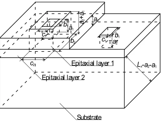
In the present paper we consider a semiconductor heterostructure, which consist of a substrate and two epitaxial layers. The epitaxial layers include into itself some area, which manufactured by using another materials (see Figs. 1 and 2). Let us consider dopants, which were infused
into the areas to produce reverse types of conductivity (p or
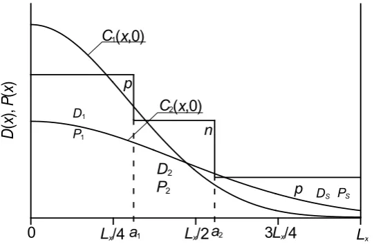
n). The types should be differing from type of conductivity of the substrate. The Figs. 3 and 4 show spatial distributions of dopants in the considered heterostructure near drain and source. Father we consider annealing of the dopants. Distributions of dopants spread during the annealing. Availability of interfaces between layers of heterostructure leads to deformation of distributions of dopants in comparison with the distributions in homogenous sample. We obtain increasing of sharpness of p-n-junctions and homogeneity of dopant distributions in doped area. Main aim of the present paper is formulating of recommendations to manufacture transistors with as small as possible their dimensions framework configuration in Figs. 1 and 2.
2. Method of Solution
Let us determine spatiotemporal distributions of dopants to solve our aim. We calculate the distributions of dopants by calculation of solution of the second Fick’s law [8,9]
(
)
(
)
(
)
+
+
=
y
t
z
y
x
C
D
y
x
t
z
y
x
C
D
x
t
t
z
y
x
C
C
C
∂
∂
∂
∂
∂
∂
∂
∂
∂
∂
,
,
,
,
,
,
,
,
,
(
)
+
z t z y x C D
z C
∂
∂
∂
∂
, , ,Figure 1. Heterostructure with a substrate and two epitaxial layers. The epitaxial layers include into itself some area, which manufactured by using another materials
Figure 2. Profile of side elevation drawing of the obtained heterostructure
Figure 3. Distribution of dopant near drain
c1
a2
b1
L
x-
a2-
a
1a1
c1
b
1c
2a
+
a
21
a1
b
2Substrate
Epitaxial layer 2
Epitaxial layer 1
a
1
a
2
L
x-a
2
-a
1
c1
c1
c2
oxide source
drain gate
D
(
x
),
P
(
x
)
C
(
x
,0)
D
1P
1D
SP
SL
xa
10
L
x/4
L
x/2
3
L
x/4
p
[image:2.595.165.451.73.286.2] [image:2.595.147.462.328.738.2] [image:2.595.172.442.538.734.2]Figure 4. Distributions of dopants near source with boundary and initial conditions
(
,
,
,
)
0
0
=
∂
∂
= x
x
t
z
y
x
C
,
∂
(
∂
,
,
,
)
=
0
=Lx
x
x
t
z
y
x
C
,
(
, , ,)
00 = ∂
∂
= y y
t z y x C
, (2)
(
,
,
,
)
=
0
∂
∂
=Ly
x
y
t
z
y
x
C
,
(
,
,
,
)
0
0
=
∂
∂
= z
z
t
z
y
x
C
,
(
,
,
,
)
=
0
∂
∂
=Lz x
z
t
z
y
x
C
, C (x,y,z,0)=f (x,y,z).
Here C(x,y,z,t) is the spatiotemporal distribution of concentration of dopant, T is the temperature of annealing, DС is the dopant diffusion coefficient. Value of the dopant diffusion coefficient depends on properties of materials of heterostructure, speed of heating and cooling heterostructure (according to Arrhenius law). Dependences of dopant diffusion coefficient on parameters could be approximated by the following function [9]
(
)
(
(
)
)
+
=
T
z
y
x
P
t
z
y
x
C
T
z
y
x
D
D
C L,
,
,
1
γ,
,
,
,
,
,
γ
ξ
. (3)Here DL(x,y,z,T) is the spatial (due to inhomogeneity of heterostructure) and temperature (due to Arrhenius law) dependences of dopant diffusion coefficient; P(x,y,z,T) is the limit of solubility of dopant; parameter γ depends on properties of materials and could be integer usually in the following interval γ ∈[1,3] [9]. Concentrational dependence of dopant diffusion coefficient is discussed in details in the Ref. [9].
We determined the spatiotemporal distribution of concentration of dopant by method of averaging of function corrections [10] with decreased quantity of iteration steps [11]. Framework the approach we consider solution of Eq.(1) with averaged value of diffusion coefficient D0 as the first-order approximation of concentration of dopant. The solution could be written in the form
(
)
=
∑
∞( ) ( ) ( ) ( )
=1
1
,
,
,
2
n nC n n n n
z y x
t
e
z
c
y
c
x
c
F
L
L
L
t
z
y
x
C
π
,
where
( )
+
+
−
=
exp
2 2 01
21
21
2z y x
n
t
n
D
t
L
L
L
e
π
;=
L∫
x( ) ( ) ( ) (
∫
y∫
z)
L L
C n n n
nC
c
u
c
v
c
w
f
u
v
w
d
w
d
v
d
u
F
0 0 0
,
,
; s=x,y,z; cn(s)=cos
(πns/Ls).
We determine approximations of concentration of dopant with order n=2 and higher framework standard iterative procedure of method of averaging of function corrections [10]. Framework the approach to determine the approximation with order n we replace the definiendum function C(x,y,z,t) in the right side of the Eq. (1) on the sum of the average value αn of the approximation with order n and the approximation with order n-1, i.e. C(x,y,z,t)→αn+Cn-1(x,y,z, t). The replacement leads to transformation of the Eq.(1) to equation for the equation for the approximation with order n of dopant concentration. For n= 2 we obtain
D
(
x
),
P
(
x
)
C
1(x
,0)
D1
P1
DS PS
L
xa
10
L
x/4
L
x/2
a
23L
x/4
D
2P
2C
2(x,0)
p
n
[image:3.595.172.443.74.254.2](
)
(
)
[
(
)
]
(
)
(
)
+ + + = x t z y x C T z y x P t z y x C T z y x D x t t z y x C L ∂ ∂ α ξ ∂ ∂ ∂ ∂ γγ , , ,
, , , , , , 1 , , , , ,
, 2 1 1
2
(
)
[
(
(
)
)
]
(
)
+
+
+
+
y
t
z
y
x
C
T
z
y
x
P
t
z
y
x
C
T
z
y
x
D
y
L∂
∂
α
ξ
∂
∂
γγ
,
,
,
,
,
,
,
,
,
1
,
,
,
2 1 1(4)
(
)
[
(
(
)
)
]
(
)
+ + +zy z t x C T z y x PC x y z t T
z y x D
z L
∂
∂
α
ξ
∂
∂
γ γ , , , , , , , , , 1 , ,, 2 1 1
.
Integration of left and right sides of Eq. (4) gives us possibility to obtain relation for the second-order approximation of dopant concentration in the final form
(
)
(
)
[
(
(
)
)
]
(
)
+
∫
+
+
=
t Ld
x
z
y
x
C
T
z
y
x
P
z
y
x
C
T
z
y
x
D
x
t
z
y
x
C
0 1 1 22
,
,
,
,
,
,
1
,
,
,
,
,
,
∂
,
,
,
τ
τ
∂
τ
α
ξ
∂
∂
γ γ(
)
[
(
(
)
)
]
(
)
+ ∫ + ++ t L d
y z y x C T z y x P z y x C T z y x D y 0 1 1
2 , , ,
, , , , , , 1 , , , τ ∂ τ ∂ τ α ξ ∂ ∂ γ γ (4a)
(
)
[
(
(
)
)
]
(
)
d f(
x y z)
zy z
x C T z y x
PC x y z
T z y x D z t
L , , , , ,
, , , , , , 1 , , , 0 1 1 2 + ∫ + + + τ ∂ τ ∂ τ α ξ ∂ ∂ γ γ
We determine the average value α2 by standard relation [10]
(
)
(
)
[
]
∫ ∫ ∫ ∫
−
Θ
=
Θ0 0 0 0 2 1
2
1
,
,
,
,
,
,
x y z L L L
z y x
t
d
x
d
y
d
z
d
t
z
y
x
C
t
z
y
x
C
L
L
L
α
. (5)Substitution of the relation (4a) into relation (5) gives us possibility to obtain the relation for the definiendum value α2
(
)
∫ ∫ ∫ ∫
Θ
=
Θ0 0 0 0
2
1
,
,
x y z
L L L
z y x
t
d
x
d
y
d
z
d
z
y
x
f
L
L
L
α
.
Analysis of the spatiotemporal distribution of concentration of dopant has been done analytically by using the second-order approximation of the concentration, which has been calculated framework the method of averaging of function correction. The approximation is enough good approximation to make qualitative analysis and to obtain some quantitative results. The results of analytical calculations have been checked by comparison of the results with results of numerical simulation.
3. Discussion
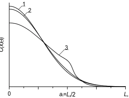
[image:4.595.149.445.77.187.2]In this section we analyzed redistribution of dopants, which have been infused in the heterostructure in Figs. 1 and 2. Typical distributions of dopant are presented in Fig. 5. The figure shows, that availability of the interface between layers of heterostructure and appropriate choosing of annealing time give us possibility to increase sharpness of p-n-junction in comparison with p-n-junction in homogenous sample. At the same time one can obtain increasing of homogeneity of dopant distribution in doped area. It is known, that increasing of annealing time leads to increasing of homogeneity of dopant distribution, but sharpness of p-n-junction decreasing. On the other hand decreasing of annealing time leads to decreasing of homogeneity of dopant distribution in doped
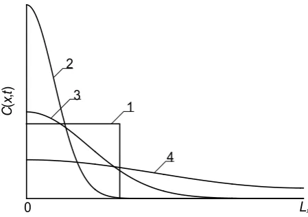
area and decreasing of effectiveness of using of interfaces between layers of heterostructure. Recently we introduce a criterion, which gives us possibility to estimate compromise annealing time [12-15]. Framework the criterion we approximate real distribution of dopant by a step-wise function (see Fig. 6). We determine the optimal annealing time by minimization of the following mean-squared error
Figure 5. Dopant distributions in a heterostructure with two layers (a substrate and an epitaxiallayer)fordifferentvaluesofdifferencebetween dopant diffusion coefficients
C
(
x
,Θ
)
0 a1=Lx
/2
Lx1 2
[image:4.595.323.547.543.713.2](
)
(
)
[
]
∫ ∫ ∫
Θ
−
=
L L Lx y zz y x
x
d
y
d
z
d
z
y
x
z
y
x
C
L
L
L
U
0 0 0
,
,
,
,
,
1
ψ
, (6) where ψ (x,y,z) is the approximation function, which presented in Fig. 6 as curve 1. Dependences of optimal annealing time on several parameters are presented in Fig. 7. It should be noted, that the first dopant (the dopant infusing near source) should be anneal during time Θ=Θ1-Θ2, where Θ1 and Θ2 are optimal annealing times for optimal annealing of the dopants, when they are independent from each other. Vales of optimal annealing times could be estimated by the following relations : Θ1=(a22/D2)+(a12/D1) and Θ2=a12/D1, where Di are dopant diffusion coefficients in appropriate materials. During infusion of dopant near drain one shall to take into account redistributions of dopants near source and synchronization with the infusion.
Figure 6. Spatial distributions of infused dopant in heterostructure. Curve 1 is required idealized distribution of dopant. Curves 2-4 are real
distributions of infused dopant in heterostructure for different values of annealing time (increasing of number of curve corresponds to increasing of annealing time)
4. Conclusion
In this paper we introduce an approach to manufacture more compact field-effect transistors in comparison with recently introduced configurations. The approach bases on infusion of dopants in a semiconductor heterostructure and optimization of annealing time. At the same time with decreasing of dimensions the introduced approach to manufacturing of the field-effect transistors gives us possibility to simplify their configuration in comparison with recently introduced one [16,17]. The simplification leads to decreasing of price of manufacturing of field-effect transistors.
Figure 7 Dependences of dimensionless optimal annealing time of dopant, infused in heterostructure in Figs. 1 and 2, which have been calculated by minimization the mean squared error Eq. (6) on several parameters. Curve 1 is the dependence of optimal annealing time on the ratio a1/Lx (dependence of optimal annealing time on the ratio a2/Lx is
the similar to the dependence on a1/Lx) for pairwise equality of dopant diffusion coefficients and ξ=γ=0. Curve 2 is the dependence of optimal annealing time on the relation (D1/DS–1) for a1/Lx=1/2 (dependence of optimal annealing time on the ratio (D2/DS–1) is the similar to the dependence on (D1/DS–1)), ξ=γ=0. Curve 3 is the dependence of optimal annealing time on the parameter ξ for pairwise equality of dopant diffusion coefficients and a1/Lx=1/2, γ=0. Curve 4 is the dependence of optimal annealing time on the parameter γ
for pairwise equality of dopant diffusion coefficients and
[image:5.595.320.544.215.387.2]a1/Lx=1/2, ξ=0
Figure 7
Acknowledgments
This work is supported by the contract 11.G34.31.0066 of the Russian Federation Government and educational fellowship for scientific research.
[1] A. Kerentsev, V. Lanin, Power Electronics, Issue 1. P. 34 (2008).
[2] A.O. Ageev, A.E. Belyaev, N.S. Boltovets, V.N. Ivanov, R.V. Konakova, Ya.Ya. Kudrik, P.M. Litvin, V.V. Milenin, A.V. Sachenko. Semiconductors. Vol. 43 (7). P. 897-903 (2009). [3] Jung-Hui Tsai, Shao-Yen Chiu, Wen-Shiung Lour, Der-Feng
Guo. Semiconductors. Vol. 43 (7). P. 971-974 (2009). [4] E.I. Gol’dman, N.F. Kukharskaya, V.G. Naryshkina, G.V.
Chuchueva. Semiconductors. Vol. 45 (7). P. 974-979 (2011). [5] T.Y. Peng, S.Y. Chen, L.C. Hsieh C.K. Lo, Y.W. Huang,
W.C. Chien, Y.D. Yao. J. Appl. Phys. Vol. 99 (8). P. 08H710-08H712 (2006).
[6] W. Ou-Yang, M. Weis, D. Taguchi, X. Chen, T. Manaka, M. Iwamoto. J. Appl. Phys. Vol. 107 (12). P. 124506-124510 (2010).
[7] J. Wang, L. Wang, L. Wang, Z. Hao, Yi Luo, A. Dempewolf, M. M
u
ller, F. Bertram, Ju
rgen Christen. J. Appl. Phys. Vol. 112 (2). P. 023107-023112 (2012).[8] A.B. Grebene. Bipolar and MOS analogous integrated circuit design. New York, John Wyley and Sons, 1983, 894p.
C
(
x
,
t
)
0 Lx
2
1 3
4
0.0 0.1 0.2 0.3 0.4 0.5
a/L, ξ, ε, γ
0.0 0.1 0.2 0.3 0.4 0.5
Θ
D0
L
-2
3 2
4
[image:5.595.65.290.287.445.2][9] Z.Yu. Gotra, Technology of microelectronic devices (Radio and communication, Moscow, 1991, in Russian).
[10] Yu.D. Sokolov. Applied Mechanics. Vol.1 (1). P. 23-35 (1955).
[11] E.L. Pankratov. Eur. Phys. J. B. Vol. 57 (3). P. 251-256 (2007).
[12] E.L. Pankratov. Phys. Rev. B. V.72 (7). P. 075201-075208 (2005).
[13] E.L. Pankratov. Phys. Lett. A. Vol. 372 (11). P. 1897-1903 (2008).
[14] E.L. Pankratov. Proc. of SPIE. Vol. 7521, 75211D (2010). [15] E.L. Pankratov, E.A. Bulaeva. Applied Nanoscience (in
press).
[16] E.L. Pankratov. J. Comp. Theor. Nanoscience. Vol. 9 (12). P. 2166-2171 (2012).