I n t e r n a t i o n a l J o u r n a l o f E n g i n e e r i n g R e s e a r c h a n d S p o r t s S c i e n c e Page1
Vasujadevi Midasala Assistant Professor, Chalapathi Institute of Engineering & Technology, Guntur, A.P.,INDIA S Nagakishore
Bhavanam
Assistant Professor, University College of Engineering & Technology,Acharya Nagarjuna University, Guntur, A.P.,INDIA
ABSTRACT
The memory blocks testing is a separate testing procedure followed in VLSI testing. The memory blocks testing involve writing a specific bit sequences in the memory locations and reading them again. This type of test is called March test. A particular March test consists of a sequence of writes followed by reads with increasing or decreasing address. For example the March C- test has the following test pattern. There are several test circuits available for testing the memory chips. However no test setup is developed so far for testing the memory blocks inside the FPGA. The BRAM blocks of FPGA are designed to work at much higher frequency than the FPGA core logic. Hence testing the BRAMs at higher speed is essential. The conventional memory test circuits cannot be used for this purpose. Hence the proposed work develops a memory testing tool based on March tests for FPGA based BRAM (block RAM testing). The code modules for March test generator shall be developed in VHDL and shall be synthesized for Xilinx Spartan 3 Family device. A PC based GUI tool shall send command to FPGA using serial port for selecting the type of test. The FPGA core gets the command through UART and performs the appropriate and sends the test report back to PC. The results shall be verified in simulation with Xilinx ISE simulator and also in hardware by using Chip scope. Xilinx Spartan 3 family FPGA board shall be used for hardware verification of the developed March test generator.
__________________________________________________________________________________________________________
I. INTRODUCTION
The cost of verification and test for nowadays circuits represents an important part of the total IC final price. Hence, the domain of test represents a cornerstone for the industry. Recently, the advances in semiconductor memory technologies have become more complex resulting in a rapidly increasing transistor per memory design. New design techniques enable a higher memory capacity implementation on a fixed die size. However, larger memory capacities require more extensive testing. Inevitably memory testing time increases the fault model to effectively model the variety of physical failures that could occur because of interference between closely packed cells. On the other hand, the more compact size will produces more defects during chip manufacturing, pushing yields down.
Therefore, memory testing and repairing will be more important in the future memory chips. Testing and diagnosis techniques play a key role in the advancement of semiconductor memory technologies. The challenge in obtaining reliable failure detection has created intensive investigation on efficient testing and diagnosis algorithms for better fault coverage and diagnostic resolution. There are a number of test techniques that have been well studied. Many test algorithms were proposed based on functional-level fault models using manual technique analysis. Although March Test Algorithm (MTA) is one of the best solutions and widely use in testing memories, due to the technology advance there are more new fault models will be introduced. Therefore, to
overcome this coming fault models a new technique is required to develop which can be automatically analyzed and added the new technique. This paper aims to propose a new solution for researchers and engineers to find an efficient test and diagnosis algorithm in shorter time. A combination march-based test algorithm will be implemented for this purpose. Universities and industry involved in memory Built-in-Self test, Built-in- Self repair and Built-Built-in-Self diagnose will benefit by saving a few years on research and development due to the fact that the manual and automatic test procedures developed in this work is compatible an expandable for BRAM Memory testing [1] .
II. MARCH TEST
Test sequences or test algorithms for memories are known under the name of March tests. Every March test has specific capabilities that allow revealing the typical defects of memories. A March test consists of a sequence of March elements. A March element has a certain number of operations (or March primitive) that must be applied to all memory cells of an array. Thus, ↑(r0;w 1) is a March element and r0 and w1
are March primitives. A March element is specified by an address order and a number of Read/Write operations. The addressing order of a March element can be done in an up (↑),
down (↓) way or (↕) if the order is not significant. A March
primitive can be a write 1 (w1), write 0 (w0), read 1(r1) and read 0 (r0) that can be performed in a memory cell.
The test is "marching" through the memory.
FAULT DIAGNOSIS IN MEMORY CHIPS USING
FPGA - BY COMPLEX TEXT PATTERN
GENERATION
ENGINEERING
I n t e r n a t i o n a l J o u r n a l o f E n g i n e e r i n g R e s e a r c h a n d S p o r t s S c i e n c e Page2
The test is composed of March elements represented between ().
March tests are the simplest tests (optimal) to detect most of the functional faults.
March Test Notation
↑: address sequence is in the ascending order from cell 0 to
cell n-1.
↓: address changes in the descending order from cell n-1 to cell 0.
↕: address sequence is either ↑ or ↓.
r: the Read operation.
Special Test For Memories (March Test)
Memories are built with separate VLSI technology and very sensitive CMOS Cells.
Following faults are usually noticed in faulty Memory cells.
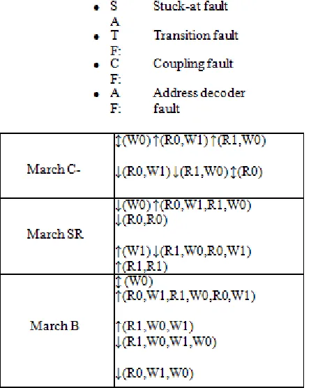
Table.1: March test sequences
The above table shows the implemented March test sequences. If a memory block gets through all these three test sequences, we can say that the memory block is fault free. Here the Block RAM is treated as IPCore of 16 bit width and depth of 256, which is generated by Xilinx CoreGen with Single port configuration.
To declare a memory circuit is functionally working we need to create conditions to diagnosis above said faults.
III. FPGA IMPLEMENTATION FOR MARCH TEST GENERATOR
The implementation part develops a test bench architecture for Block RAMs, is composed of one computer, a March test generator, a serial interface (for communication between the March test generator and computer) and Block RAMs on FPGA as shown in Figure 3.1
Figure 3.1: Test bench architecture
Memory blocks are fabricated using high dense circuits, transistors are closely packed, and intentionally they are very sensitive devices and work with very high speed read & write sequences.
When shipping out from the factory, that time they definitely do testing.
When deployed into some field, there years together these have to work.
Block RAM is a block on FPGA which will be always in usage.
First keeping in BRAM and reading in an FPGA. Hence BRAM is always active.
Here there is a need to test BRAM logic whether it is working correctly or not.
FPGA core is capable of running at 50MHz but the BRAM capable of running at200MHz.
Something running at higher frequency means it is sensitive and assertable to errors.
Certain errors will come out when you run at higher clock frequency.
Over aging errors are introduced in BRAM.
IV. EXPERIMENTAL RESULTS
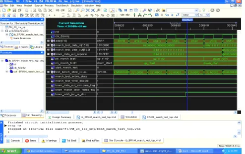
The following chapter consists of all the software and hardware results observed in the project. The results include snapshots of each and every module individually with all the inputs, outputs and intermediate waveforms.
4.1 Simulation Results
The written input values into BRAM are read with expected values.
Here the contents of BRAM are read without any failure. Hence March test C- is Successful and BRAM is fault
I n t e r n a t i o n a l J o u r n a l o f E n g i n e e r i n g R e s e a r c h a n d S p o r t s S c i e n c e Page3
Figure 4.1: Data output of BRAM using March-C
Figure 4.2: Data output of BRAM using March C- with Fault insertion
The written input values into BRAM are read with expected values except at address “aa”.
Here the contents of BRAM are read with fault. Hence March test C- is Successful and BRAM is faulty.
Figure 4.3: Data output of BRAM Using March SR
The written input values into BRAM are read with expected values.
Here the contents of BRAM are read without any failure. Hence March SR test is Successful and BRAM is fault
Free.
Figure 4.4: Data output of BRAM using March SR with Fault insertion address “aa”.
The written input values into BRAM are read with expected values except at
Here the contents of BRAM are read with fault.
Hence March SR test is Successful and BRAM is faulty.
Figure 4.5: Data output of BRAM using March B The written input values into BRAM are read with
expected values.
Here the contents of BRAM are read without any failure. Hence March B test is Successful and BRAM is fault
Free.
I n t e r n a t i o n a l J o u r n a l o f E n g i n e e r i n g R e s e a r c h a n d S p o r t s S c i e n c e Page4
The written input values into BRAM are read with expected values except at address “aa”.
Here the contents of BRAM are read with fault. Hence March B test is Successful and BRAM is faulty.
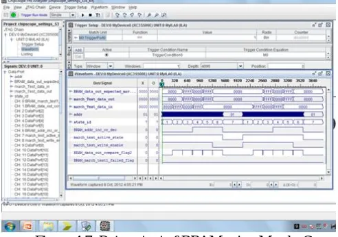
4.2 Chipscope Results
Figure 4.7: Data output of BRAM using March -C
Figure 4.8: Data output of BRAM using March C- with Fault insertion
Figure 4.9: Data output of BRAM using March SR
Figure 4.10: Data output of BRAM using March SR with Fault insertion
Figure 4.11: Data output of BRAM using March B
I n t e r n a t i o n a l J o u r n a l o f E n g i n e e r i n g R e s e a r c h a n d S p o r t s S c i e n c e Page5
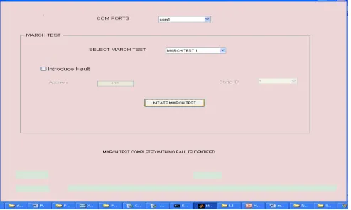
4.3 Results Of Integrated Top Module With GUI
Fault diagnosis using March C- test
Figure 4.13: Without Fault insertion
Figure 4.14: With Fault insertion
Fault Diagnosis using March SR test
Figure 4.15: Without Fault insertion
Figure 4.16: With Fault insertion
Fault Diagnosis Using March B Test
Figure 4.17: Without Fault insertion
V. CONCLUSION
With technology scaling, process variations result in functional failures in memory systems. In this work, physical failure mechanisms in BRAM on FPGA boards are analyzed and classified into the established logic fault models. March test sequences are compared and optimized to target these emerging failure mechanisms. March C- test sequence, the memory test time is reduced.
REFERENCES
[1] Semiconductor Industry Association (SIA), "International Technology
Roadmap for Semiconductors (ITRS) ", 2005 edition
[2] A. Bosio et al., "Interactive Educational tool for Memory Testing,
"pp.100-103, 6th International Workshop on Microelectronics
Education, 2006
[3] A.J. Van de Goor, "Testing Semiconductor Memories: Theory and
Practice, " John Wiley & Sons, ISBN 0-471-92586-1, 1991
[4] P. Rech et al., "A Memory Fault Simulator for Radiation-Induced
Effects in SRAMs," IEEE 19th Asian Test Symposium,2010
[5] S. Borkar, T. Karnik, S. Narendra, J. Tschanz, A. Keshavarzi, and V. De, “Parameter variations and impact on circuits and microarchitecture,” in Proc. Design Automation Conf., Jun. 2003, pp. 338–342
I n t e r n a t i o n a l J o u r n a l o f E n g i n e e r i n g R e s e a r c h a n d S p o r t s S c i e n c e Page6
industry association.
[7] Q. Chen, H. Mahmoodi, S. Bhunia, and K. Roy, “Modeling and testing
of SRAM for new failure mechanisms due to process variations in nanoscale CMOS,” in Proc. VLSI Test Symp., sec. 8b, May 2005, pp.292–297.
[8] C.A. Papachristou and N.B.Saghal, "An Improved Method for Detecting
Functional Faults in Random Access Memories", IEEE Trans. Computers, Vol. C-34, No. 2, 1985, pp.110-116.
[9] A.J. van de Goor, Testing Semiconductor Memories, Theory and
Practice, John Wiley & Sons, Chichester, UK, 1991.
[10] S. Borkar et al., “Parameter Variations and Impact on Circuits and
Microarchitecture”, DAC 2003, pp. 338-342.
[11] S. Hamdioui et al., “Linked Faults in Random Access Memories:
Concept, Fault Models, Test Algorithms, and Industrial Results,” IEEE TCAD, May 2004.
[12] S. Hamdioui et al., “Experimental analysis of spot defects in SRAMs: