Volume 1; Issue 2; Page No. 74-80
e
74
Algorithm and Architecture for a Low-Power Content Addressable Memory Based on
Sparse Compression Technique
Dr.S.Muthukrishnan
1, Anto Yohan
2, T.Janani
3HOD-ECE, Sri Eshwar College of Engineering, Kinathukadavu, Coimbatore1
Chief Executive, Robosoft Technology, Coimbatore2
PG Scholar, Sri Eshwar College of Engineering, Kinathukadavu, Coimbatore3
Email Id:[email protected],
Abstract
We propose an extended versions are presented that elaborates the effect of the design’s degrees of freedom, and the effect on non uniformity of input patterns on energy consumption and the performance. The proposed architecture is based on a recently refined sparse clustered networks using binary connections that on-average eliminates most of the parallel comparisons performed during a search. Given an input tag, the proposed architecture computes a few possibilities for the location of the matched tag and performs the comparisons on them to locate a single valid match. And also by using a reordered overlapped search mechanism, most mismatches can be found by searching a few bits of a search word. Following a selection of design parameters, such as the number of CAM entries, the energy consumption and the search delay of the proposed design are 8%, and 26% of that of the conventional NAND architecture, respectively, with a 10% area overhead.
Key Words: Associative memory, content-addressable memory (CAM), low-power computing, recurrent neural
networks, binary connections, sparse clustered networks (SCNs).SCN-Based classifier.
1. Introduction
Acontent addressable memory (CAM) is a type of memory that can be accessed using its contents rather than an explicit address. In order to access a particular entry in such memories, a search data word is compared against previously stored entries in parallel to find a match. Each stored entry is associated with a tag that is used in the comparison process. Once a search data word is applied to the input of a CAM, the matching data word is retrieved within a single clock cycle if it exists. This prominent feature makes CAM a promising candidate for applications where frequent and fast look-up operations are required, such as in translation look-aside buffers (TLBs) , network routers, database accelerators, image processing, parametric curve extraction, Hough transformation , Huffman coding/decoding, virus detection, Lempel–Ziv compression, and image coding. Due to the frequent and parallel search operations, CAMs consume a significant amount of energy. CAM architectures typically use highly capacitive search lines (SLs) causing them not to be energy efficient when scaled. For example, this power inefficiency has constrained TLBs to be limited to no more than 512 entries in current processors. In Hitachi SH-3 and Strong ARM embedded processors, the fully associative TLBs consume about 15% and 17% of the total chip power, respectively. Consequently, the main research objective has been focused on reducing the energy consumption without compromising the throughput. Energy saving opportunities have been discovered by employing either circuit-level techniques, architectural-level techniques.
A new family of associative memories based on sparse clustered networks (SCNs) has been recently introduced and implemented using field-programmable gate arrays (FPGAs). Such memories make it possible to store many short messages instead of few long ones as in the conventional Hopfield networks with significantly lower level of computational complexity. Furthermore, a significant improvement is achieved in terms of the number of information bits stored per memory bit (efficiency).
e
75
e
75
e75
e
75
e75
e
75
e75
e
75
e75
e
75
e
75
e
75
e
75
e75
e
75
e75
e
75
e75
e
75
e75
e
75
very few sub-blocks of the CAM to be activated. Once the sub-blocks are activated, the tag is compared against the few entries in them while keeping the rest deactivated and thus lowers the dynamic energy dissipation.
2. CAM Review
In a conventional CAM array, each entry consists of a tag that, if matched with the input, points to the location of a data word in a static random access memory (SRAM) block. The actual data of interest are stored in the SRAM and a tag is simply a reference to it. Therefore, when it is required to search for the data in the SRAM, it suffices to search for its corresponding tag. Consequently, the tag may be shorter than the SRAM-data and would require fewer bit comparisons. An example of a typical CAM array, consisting of four entries having 4 bits each, is shown in Fig. 1. A search data register is used to store the input bits. The register applies the search data on the differential SLs, which are shared among the entries. Then, the search data are compared against all of the CAM entries. Each CAM-word is attached to a common match line (ML) among its constituent bits, which indicates, whether or not, they match with the input bits. Since the MLs are highly capacitive, a sense amplifier is typically considered for each ML to increase the performance of the search operation.
A BCAM cell is typically the integration of a 6-transistor (6T) SRAM cell and comparator circuitry. The comparator circuitry is made out of either an XNOR or an XOR structure, leading to a NAND-type or a NOR-type operation, respectively. The selection of the comparing structure depends on the performance and the power requirements, as a NAND-type operation is slower and consumes less energy as opposed to that of a NOR type.
Fig.2.The schematic of two types of typical BCAM cells.
In a NAND-type CAM, the MLs are precharged high during the precharge phase. During the evaluation phase, in the case of a match, the corresponding ML is pulled down though a series of transistors [M5 in Fig. 2(b)] performing a login NAND in the comparison process. In a NOR-type CAM [Fig. 2(a)], the MLs are also precharged high during the precharge phase. However, during the evaluation phase, all of the MLs are pulled down unless there is a matched entry such that the pull-down paths M3 − M4 and M5 − M6 are disabled. Therefore, a NOR-type CAM has a higher switching activity compared with that of a NAND type since there are typically more mismatched entries than the matched ones.
3. Related Work
Energy reduction of CAMs employing circuit-level techniques are mostly based on the following strategies: 1) reducing the SL energy consumption by disabling the precharge process of SLs when not necessary and 2) reducing the ML precharging, for example, by segmenting the ML, selectively precharging the first few segments and then propagating the precharge process if and only if those first segments match. This segmentation strategy increases the delay as the number of segments is increased. A hybrid-type CAM integrates the low-power feature of NAND type with the high-performance NOR type while similar to selective precharging method, the ML is segmented into two portions. The high-speed CAM designed in 32-nm CMOS achieves the cycle time of 290 ps using a swapped CAM cell that reduces the search delay while requiring a larger CAM cell (11-transistors) than a conventional CAM cell [9-transistors (9T)] used in SCN-CAM. A high-performance AND-type match-line scheme is proposed in [32], where multiple fan-in AND gates are used for low switching activity along with segmented-style match-line evaluation to reduce the energy consumption.
e
76
e
76
e76
e
76
e76
e
76
e76
e
76
e76
e
76
e
76
e
76
e
76
e76
e
76
e76
e
76
e76
e
76
e76
e
76
In the proposed design, we demonstrate how it is possible to reduce the number of comparisons to only N bits. Furthermore, in PB-CAM, the increase of the tag length affects the energy consumption, the delay, and also complicates the precomputation stage.
4. SCN-CAM Algorithm
Fig. 3. Top level block diagram of SCN-CAM.
As shown in Fig. 3, the proposed architecture (SCN-CAM) consists of an SCN-based classifier, which is connected to a special-purpose CAM array. The SCN-based classifier is at first trained with the association between the tags and the address of the data to be later retrieved.
The proposed CAM array is based on a typical architecture, but is divided into several sub-blocks that can be compare-enabled independently. Therefore, it is also possible to train the network with the association between the tag and each CAM sub-block if the number of desired sub-blocks is known. However, in this paper, we focus on a generic architecture that can be easily optimized for any number of CAM sub-blocks. Once an input tag is presented to the SCN-based classifier, it predicts which CAM sub-block(s) need to be compare-enabled and thus saves the dynamic power by disabling the rest. Disabling a CAM sub-block avoids charging its highly capacitive SLs, while applying the search data, and also turns the precharge path off for the MLs.
A.SCN-Based Classifier
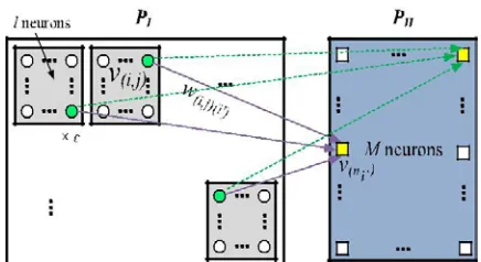
SCN-Based Classifier is used for either training or decoding purposes, the input tag is reduced in length to q bits, and then divided into c equally.
Fig. 4. Representation of the proposed SCN-CAM.
e
77
e
77
e77
e
77
e77
e
77
e77
e
77
e77
e
77
e
77
e
77
e
77
e77
e
77
e77
e
77
e77
e
77
e77
e
77
B. Tag-Length Reduction
Given the input tags, the number of bits in the reduced-length tag, q, determines the number of possible ambiguities in PII. The generated ambiguities can be corrected with additional comparisons to find the exact match in the CAM. Therefore, no errors are produced in determining the matched result(s).
5. Circuit Implementation
In order to implement a circuit that can elaborate the benefit of the proposed algorithm, a set of design points were selected among 15 different parameter sets with the common goal of discovering the minimum energy consumption per search, while keeping the silicon-area overhead and the cycle time reasonable.
Fig. 5. Relationship between the length of the truncated tag (q), the number of matched entries in SCN-CAM (λ), and the estimated matching probability (P (λ)) for M = 512.
Fig. 5 shows simulations results on how it is possible to reduce the estimated number of required comparisons by increasing q. It is interesting to note that the number of clusters in PI does not affect the number of neurons.
A drawback of such methods, unlike SCN-CAM, is that as the length of the tags is increased, the cycle time and the circuit complexity of the precomputation stage are dramatically increased.
A. SCN-CAM: Architecture of SCN-Based Classifier
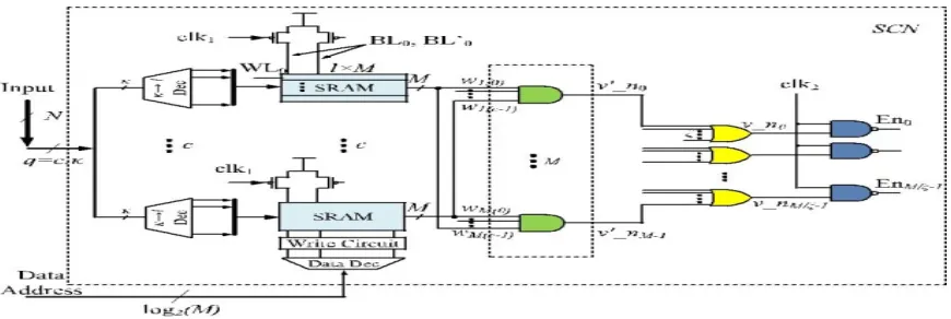
The SCN-based classifier in SCN-CAM architecture generates the compare-enable signal(s) for the CAM sub-blocks attached to it. The architecture of the SCN-based classifier is shown in Fig. 6. It consists of cκ -to-l one-hot decoders, c SRAM modules of size l × M each, M c−inputANDgates, M/ζ ζ −input ORgates, andM/ζ 2-inputNANDgates. Each row of an SRAM module stores the connections from one tag to its corresponding output neuron. Each reduced-length tag of length q is thus divided into c subtags of κ bits each, where each subtag creates the row address of each SRAM module.
Fig.6.
Simplified SCN-CAM architecture.B. SCN-CAM: CAM Architecture
e
78
e
78
e78
e
78
e78
e
78
e78
e
78
e78
e
78
e
78
e
78
e
78
e78
e
78
e78
e
78
e78
e
78
e78
e
78
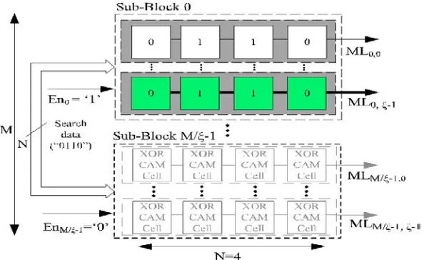
into sufficient number of compare-enabled sub-blocks such that: 1) the number of sub-blocks are not too many to expand the layout and to complicate the interconnections and 2) the number of sub-blocks should not be too few to be able to exploit to energy-saving opportunity with the SCN-based classifier. Fig.7 shows the simplified array organization for CAM architecture.
Fig .7.Simplified array organization of the proposed CAM architecture.
6. Circuit Evaluation
A complete circuit for SCN-CAM was implemented and simulated using HSPICE and TSMC 65-nm CMOS technology according to design parameters, including full dimensions of CAM arrays, SRAM arrays, logical gates, and extracted parasitics from the wires in the physical layout.
Fig. 8 shows the cycle time is measured by the maximum reliable frequency of operation in the worst-case cycle time (SS) scenario. The required silicon area of SCN-CAM is estimated to be 10.1% larger than that of the conventional NAND-type counterpart mainly due to the existence of the gaps between the SRAM blocks of the SCN-based classifier.
e
79
e
79
e79
e
79
e79
e
79
e79
e
79
e79
e
79
e
79
e
79
e
79
e79
e
79
e79
e
79
e79
e
79
e79
e
79
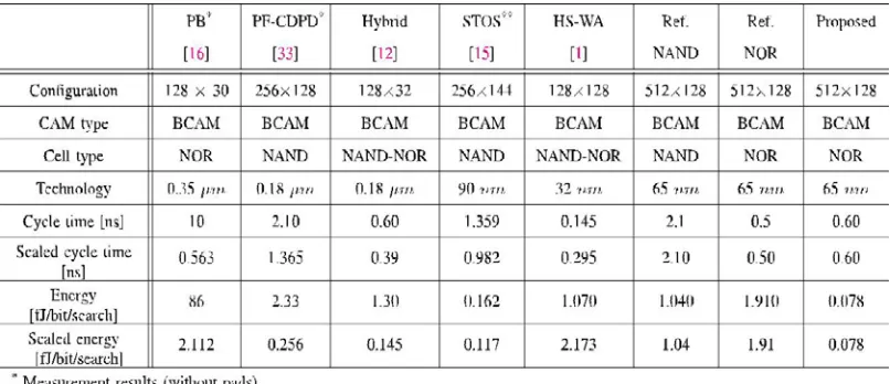
Table 1: Simulation Results.
7. Acknowledgement
The authors acknowledge the contributions of the students, faculty of Sri Eshwar College of Engineering, Kinathukadavu for helping in the design and for tool support. The authors also thank the anonymous reviewers for their thoughtful comments That Helped To Improve This Paper.
8. Conclusion
The proposed architecture (SCN-CAM) employs a novel associativity mechanism based on a recently developed family of associative memories based on SCNs.
CAM is suitable for low-power applications, where frequent and parallel look-up operations are required. SCN-CAM employs an SCN-based classifier, which is connected to several independently compare-enabled SCN-CAM sub-blocks, some of which are enabled once a tag is presented to the SCN-based classifier. By using independent nodes in the output part of SCN-CAM’s training network, simple and fast updates can be achieved without retraining the network entirely. The nonuniform inputs may result in higher power consumptions, but does not affect the accuracy of the final result. In other words, a few false-positives may be generated by the SCN-based classifier, which are then filtered by the enabled CAM sub-blocks. Therefore, no false-negatives are ever generated.
Conventional NAND-type and NOR-type architectures were also implemented in the same process technology to compare SCN-CAM against, along with other recently developed CAM architectures. It has been estimated that for a case study design parameter, the energy consumption and the cycle time of SCN-CAM are 8.02%, and 28.6% of that of the conventional NAND-type architecture, respectively, with a 10.1% area overhead. Future work includes investigating sparse compression techniques for the matrix storing the connections in order to further reduce the area overhead.
9. References
[1]. A. Agarwal et al., “A 128×128 b high-speed wide-and match-line content addressable memory in 32 nm CMOS,” in Proc. ESSCIRC, Sep. 2011, pp. 83–86.
[2.]. Y.-J. Chang and M.-F. Lan, “Two new techniques integrated for energy-efficient TLB design,” IEEETrans. Very Large Scale Integr. (VLSI) Syst., vol. 15, no. 1, pp. 13–23, Jan. 2007.
[3]. H. Chao, “Next generation routers,” Proc. IEEE, vol. 90, no. 9, pp. 1518–1558, Sep. 2002.
[4]. N.-F. Huang, W.-E. Chen, J.-Y. Luo, and J.-M. Chen, “Design of multi-field IPv6 packet classifiers using ternary CAMs,” in Proc. IEEE GlobalTelecommun. Conf., vol. 3. 2001, pp. 1877–1881.
[5]. M. Meribout, T. Ogura, and M. Nakanishi, “On using the CAM concept for parametric curve extraction,” IEEE Trans. Image Process., vol. 9, no. 12, pp. 2126–2130, Dec. 2000.
[6]. M. Nakanishi and T. Ogura, “A real-time CAM-based Hough transform algorithm and its performance evaluation,” in Proc. 13th Int. Conf.Pattern Recognit., vol. 2. Aug. 1996, pp. 516–521.
e
80
e
80
e80
e
80
e80
e
80
e80
e
80
e80
e
80
e
80
e
80
e
80
e80
e
80
e80
e
80
e80
e
80
e80
e
80
[8]. C.-C. Wang, C.-J. Cheng, T.-F. Chen, and J.-S. Wang, “An adaptively dividable dual-port BiTCAM for virus-detection processors in mobile devices,” IEEE J. Solid-State Circuits, vol. 44, no. 5, pp. 1571–1581, May 2009.
[9]. B. Wei, R. Tarver, J.-S. Kim, and K. Ng, “A single chip Lempel–Ziv data compressor,” in Proc. IEEE ISCAS, May 1993, pp. 1953–1955.
[10]. S. Panchanathan and M. Goldberg, “A content-addressable memory architecture for image coding using vector quantization,” IEEE Trans.Signal Process., vol. 39, no. 9, pp. 2066–2078, Sep. 1991.
[11]. T. Juan, T. Lang, and J. Navarro, “Reducing TLB power requirements,” in Proc. Int. Symp. Low Power Electron. Des., Aug. 1997, pp. 196–201.
[12]. Y.-J. Chang and Y.-H. Liao, “Hybrid-type CAM design for both power and performance efficiency,” IEEETrans. Very Large Scale Integr. (VLSI)Syst., vol. 16, no. 8, pp. 965–974, Aug. 2008.
[13]. Z. Lei, H. Xu, D. Ikebuchi, H. Amano, T. Sunata, and M. Namiki, “Reducing instruction TLB’s leakage power consumption for embedded processors,” in Proc. Int. Green Comput. Conf., Aug. 2010, pp. 477–484.
[14]. S.-H. Yang, Y.-J. Huang, and J.-F. Li, “A low-power ternary content addressable memory with Pai-Sigma matchlines,” IEEE Trans. VeryLarge Scale Integr. (VLSI) Syst., vol. 20, no. 10, pp. 1909–1913,Oct. 2012.
Dr. S. Muthukrishnan, HOD-ECE, Sri Eshwar College of Engineering (Affiliated to Anna University), kinathukadavu,
Coimbatore. His Specialization Area is VLSI Design and Embedded Systems
Mr. Anto Yohan Working in Robosoft Technology as Soft ware developer.His interested areas are
Networking,VLSI,Design and Software development.
Miss.T.Janani ,PG Scholar,Sri Eshwar College of Engineering(Affiliated to Anna