222
Copyright © 2011-15. Vandana Publications. All Rights Reserved.
Volume-5, Issue-3, June-2015
International Journal of Engineering and Management Research
Page Number: 222-228
A Novel Approach for the Design of Multiplexer based Reversible ALU
using SRM & KTR Gates
Aswin Kumar R1, Sathish K2, Theresal T3 1,2,3
ABSTRACT
In the modern digital era, Reversible logic plays an promising role as it provides the zero power dissipation during the digital operations. There are number of circuits designed by Reversible logic and possess their own importance in the digital world. A new Architecture of the Reversible Arithmetic Logic Unit, an important Component in Central Processing Unit of the quantum Computer is proposed. The design is implemented and Verified using the Altera Quartus II software.
Keywords---- Reversible ALU,Multiplexer, Adder based ALU
Department of Electronics and Communication Engineering, SRM University, Chennai, INDIA
I.
INTRODUCTION
Energy or Power dissipation is the most worsing problem in any of the Hardware design. Conventional logics are Irreversible. Reversible logic was first related to energy by Laudauer who stated that there is a small amount of heat dissipation due to the loss of one bit of the information and it will be equal to 2kTln where ‘k’ is Boltzman Constant and ‘T’ is Temperature[1]. Bennet supported this statement by stating that reversible logic gates must be used in order to eradicate the power consumption [2].
II.
REVERSIBLE LOGIC
Reversible circuits are those circuits that do not lose information and reversible computation in a system can be performed only when the system comprises of reversible gates [3]. These circuits can generate unique output vector from each input vector, and vice versa, that is, there is a one-to-onemapping between input and output vectors..A gate isreversible if the gate's inputs and outputs have a one-to-onecorrespondence, i.e. there is a distinct
output assignment for each distinct input. The conventionallogic gates such as AND, OR, and X-OR are not reversible, asthey are all multiple-input single output logic gates.
A NOT Gate is said to be reversible Reversible logic supports the process of running the system both forward and backward direction. This means that reversible computations can generate inputs from outputs, may stop and go back to any point in the computation history.. A reversible logic circuit should have the following features of Using minimum number of reversible gates, Garbage outputs, constant inputs.
In reversible logic there exists a unique one to one mapping between the input and output vectors. The unused outputs are used to maintain the reversibility of a reversible circuits and are referred as the garbage outputs[4]. Fan-out and loops are not permitted.
III.
RELATED WORK
Design of Control Unit for Low Power ALU with a Barrel Shifter Using Reversible Logic [10], Design of 32 Bit Reversible ALU [11] with 7-operations and Arithmetic & Logic Unit (ALU), Design using Reversible Control Unit [12] with 9-operations are related and recent work in the field using REVERSIBLE Logic Circuiits
The proposed Arithmetic Logic Unit acts with the help of the 2*1 Multiplexer which is achieved by the SRM Gate [5] and the full adder which is given by the reversible KTR Gate[6].
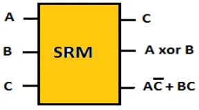
1.The Reversible SRM Gate [5]
The inputs and the outputs of the proposed 3*3 reversible SRM Gate are A,B,C and P,Q,R respectively. The simple block diagram of the proposed SRM Gate is shown in the figure 1.
223
Copyright © 2011-15. Vandana Publications. All Rights Reserved.
Figure 1 Block Diagram of the Proposed SRM Gate2. Full Adder Circuit using the KTR Gate [6]
The proposed Reversible KTR Gate acts as Full adder to exhibit the Sum and Carry when the input D is Supplied as ‘0’ as shown in the figure 2.On Implementing the Proposed KTR gate as a full adder we have 2 garbage outputs. Sum and Carry are taken in the output R and S respectively.
Figure 2.Full adder using KTR Gate
IV.
PROPOSED WORK
ALU is a data processing comp nent, which is an important part in centre process unit(CPU). Different kinds of computers have different ALUs. But all of the ALUs contain arithmetic unit and logic unit, which are the basic structures. In arithmetic operations there are add, minus, while in logical operations there are NOT, OR, AND, XOR and so on. The above operations can be realized by using reversible logic gates, through which can avoid the energy consumption. The multi-function ALU based on reversible logic gates mainly contains the reversible adder and the Multiplexer. The basic component of the arithmetic section of an ALU is a parallel adder. It consists of two sections. One is Arithmetic and the other one is Logical unit.
1.Arithmetic Unit
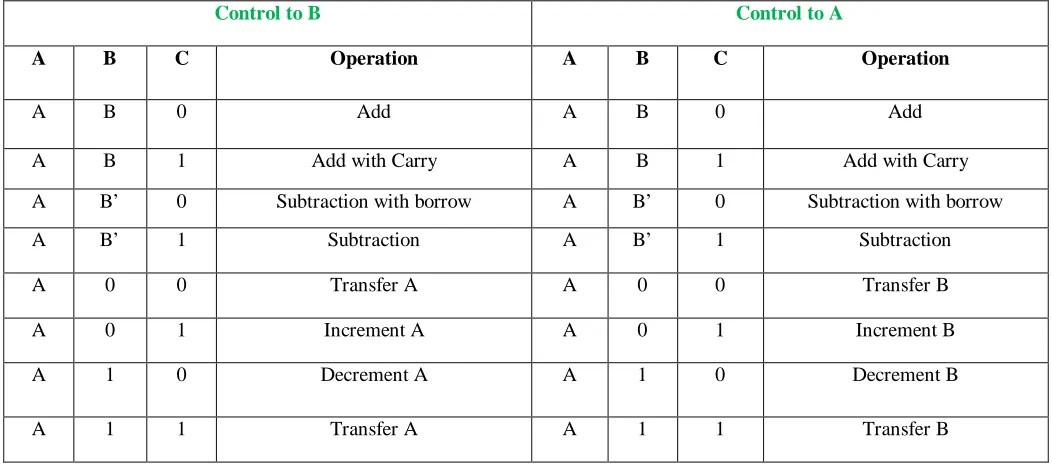
A parallel adder is constructed with a number of full adder circuits connected in cascade. By controlling the data inputs to the parallel adder, it is possible to obtain different types of arithmetic operations. Figure 4 shows the arithmetic operations obtained when one set of inputs to a parallel adder is controlled externally. The number of bits in the parallel adder may be of any value. The input carry
C in goes to the full adder circuit in the least significant bit position and the C out comes from the full adder circuit in the most significant bit position. we can obtain various type of eight operations by controlling the B input and Cin.So to design the circuit we need two parts, one is control circuit and the another one is full adder.
Figure 3 Various Eight Operations by controlling one set of the inputs to the Reversible KTR ADDER
From the figure 3, we can see various type of eight operations can be achieved by controlling the B input and C. Now other eight operations can be obtained by controlling the other set of the input A and C.
Figure 4 Control Unit with the Adder to set the control for B
These two requires the control unit that is given by the Reversible SRM Gate. Setting the controls for B of the full adder KTR Gate using the SRM Gate is given in the figure 4.
224
Copyright © 2011-15. Vandana Publications. All Rights Reserved.
Figure 5 Control Unit with the Adder to set the control forB
The Operation Table of the Setting controls to A and B is mentioned in the following table.
Table 1 Operation table by controlling the inputs A and B in the KTR Adder
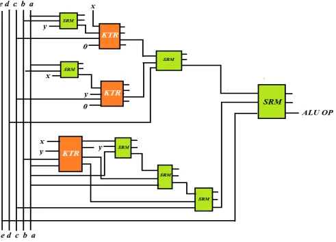
The above mentioned two blocks are further connected to a reversible SRM Multiplexer Which selects the Arithmetic value.
2.Logic Unit
The logic unit of the proposed ALU is obtained by the 2*1 Multiplexer which is given by the reversible SRM Gate. It needs the 3SRM Multiplexer. The controls are given as per the circuit diagram mentioned.
In the figure 6.Its operations includes AND, NAND, OR, NOR, EXOR, EX-NOR, and BUFFER A ,B.
3.The Proposed Multiplexer based Arithmetic and Logic Unit
The above mentioned arithmetic and the logic blocks are combined using the SRM Multiplexer and the control input is given as ‘e’ . The output of the arithmetic unit is connected to the first input of the SRM Gate and the output of the logic block is connected to the second Input of the Reversible SRM Gate. Now the proposed ALU unit will give the arithmetic operations when e= ‘0’ and it performs the Logical Operations when e= ‘1’ .The proposed ALU is given in the figure 6.
Control to B Control to A
A B C Operation A B C Operation
A B 0 Add A B 0 Add
A B 1 Add with Carry A B 1 Add with Carry
A B’ 0 Subtraction with borrow A B’ 0 Subtraction with borrow
A B’ 1 Subtraction A B’ 1 Subtraction
A 0 0 Transfer A A 0 0 Transfer B
A 0 1 Increment A A 0 1 Increment B
A 1 0 Decrement A A 1 0 Decrement B
225
Copyright © 2011-15. Vandana Publications. All Rights Reserved.
Figure 6 Proposed Arithmetic and logic unit based on SRM Multiplexer
226
Copyright © 2011-15. Vandana Publications. All Rights Reserved.
Function Table of the Proposed Multiplexer based Arithmetic and Logic Unit
Table 2 Function Table of the Proposed Multiplexer based Arithmetic and Logic Unit
V.
COMPARISON BETWEEN THE
EXISTING CONTROL UNIT AND ALU TO
THE PROPOSED MODEL
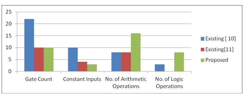
Both proposed designs are analyzed and compared in terms of number of gate count, Ancilla Inputs, No. of Arithmetic and Logic Operations, Constant Inputs.
1. Comparing the proposed ALU with the Existing ALU [10],[11]
ARITHMETIC OPERATIONS (e = 0)
d c b a Expression Operation
0 0 0 0 A Transfer A
0 0 0 1 A+1 Increment A
0 0 1 0 A+B Add
0 0 1 1 A+B+1 Add with Carry
0 1 0 0 A+B’ Subtract with borrow
0 1 0 1 A-B Subtract
0 1 1 0 A-1 Decrement A
0 1 1 1 A Transfer A
1 0 0 0 B Transfer B
1 0 0 1 B+1 Increment B
1 0 1 0 B+A Add
1 0 1 1 B+A+1 Add with Carry
1 1 0 0 A’ +B Subtract with borrow
1 1 0 1 B-A Subtract
1 1 1 0 B-1 Decrement B
1 1 1 1 B Transfer B
LOGICAL OPERATIONS (e = 1)
d c b a Operation
X 0 0 0 AND
X 0 0 1 NAND
X 0 1 0 OR
X 0 1 1 NOR
X 1 0 0 BUFFER A
X 1 0 1 EXOR
X 1 1 0 BUFFER B
227
Copyright © 2011-15. Vandana Publications. All Rights Reserved.
2. Comparing the proposed Control Unit with the Existing Control Unit [10],[11]
VI.
CIRCUIT SIMULATION & VERIFICATION
Thus the output is verified using the Modelsim Software.
VII.
CONCLUSION
In this paper, the reversible ALU design is proposed with two unique design paradigms. The proposed reversible ALU designs are verified using Altera Quartus II software. Both proposed designs are analyzed and compared in terms of number of gate count, Ancilla Inputs, No. of Arithmetic and Logic Operations, Constant Inputs.
REFERENCE
[1] R. Landauer, “Irreversibility and heat generation in the computing process,” IBM J. Res. Develop.,vol. 3, pp. 183– 191, 1961.
[2] Bennett, C.H., “Logical reversibility of Computation”, IBM J.Research and Development, 17: pp. 525-532, 1973. [3] T. Toffoli., “Reversible Computing”, Tech memo MIT/LCS/TM-151, MIT Lab for Computer Science (1980).
[4] Hafiz Md. Hasan babu, Md. Rafiqu Islam, Ahsan Raja Chowdhary and Syed Mostahead Ali chowdhary “ Reversible logic synthesis for minimization of full adder ckt”, IEEE conference on Digital system design 2003,Enro-micro‟03, Belek,Antalya,Tarkey,2003,PP 50 -54.
[5] Sathish K, Aswinkumar R,Theresal ,B.Tech Students,
Dpartment of ECE,SRM University, “A LOW POWER
REVERSIBLE BRAUN ARRAY MULTIPLIER
ARCHITECTURE USING KTR GATE” .
[6] ] Sathish K, Aswinkumar R,Theresal T, B.Tech
Students, Dpartment of ECE,SRM University , “A
Reversible Logic based Power Efficient N*1 Multiplexer Design using SRM Gate.”
228
Copyright © 2011-15. Vandana Publications. All Rights Reserved.
[8] Ann Susan Varghese, M Tech Student, Anjali V,assisstant Professor, Dept. of Electronics & Communication, Mangalam College Of Engineering, Ettumanoor, Kottayam, India, “Design of 32 Bit Reversible ALU”, , International Journal of Electronics & Communication Engineering Research (IJECER), Page: 53-56, Vol. 1 Issue 3, August – 2013.
[9] Akanksha Dixit, VinodKapse , “Arithmetic & Logic Unit (ALU) Design using Reversible Control Unit”, International Journal of Engineering and Innovative Technology (IJEIT) Volume 1, Issue 6, Page: 55-60, June 2012.
[10] Zhijin Guan,Wenjuan Li,Weiping Ding,Yueqin Hang,and Lihui Ni, “An Arithmetic Logic Unit Design Based on Reversible Logic Gates”,Communic tions ,Computers and Signal Processing (PacRim)v , pp.925-931, 03 October 2011.
[11] Akanksha Dixit, “Vinod Kapse,Arithmetic & Logic Unit (ALU) Design using Reversible Control Unit” International Journal of Engineering and Innovative Technology (IJEIT) Volume 1, Issue 6, June 2012.