Design of A Reversible Fault Tolerant Fft Using
Reversible Gates
1 Telaprolu Krishna Manoj, 2 Md.Nayeemuddin.
1M.tech-Scholar, Dept of ECE, Sri Chundi Ranganayakulu Engineering College, India. 2Assistant Professor, Dept of ECE, Sri Chundi Ranganayakulu Engineering College, India.
ABSTRACT: In this paper we are going to see the design of reversible fault tolerant architecture of FFT. This logic elements are taken from look up tables depends upon the field programmable gate array (.i.e.) FPGA. Here we are using proposed logic elements like master slave flip flop, D-Latch and multiplexer. To design the reversible fault tolerant architecture, D-Latch, master slave flip flop(MSFF) and multiplexers we propose a new fault tolerant reversible gates with FFT. Compared to the existed system this proposed system is much better and it gives better results like in terms of gates there is an increment of maximum value. There is not only increment in gates but also there is an incrementing terms of quantum cost and decrease unit delay.
KEY WORDS: FFT, master slave flip flop(MSFF), reversible logic and fault tolerant.
I.INTRODUCTION
Basically, in 1960sR. Launderer’s technical results of irreversible hardware computation show that there is energy dissipation in system which is occurring due to loss of information. Here each bit of information gets dissipated with K.T.ln2 joules of energy. Here k is the Boltzmann constant, T is the absolute temperature. At mean while in 1973, Bennett proposed a circuit to avoid the energy dissipation occurred in system. The proposed circuit consists of reversible logic gates. The main property of this proposed circuit is fault tolerance which enables a system for Continuous operation. Coming to FPGA, it contains an array of configurable logic block, interconnections and input/output blocks. The above all these are configured for every
application. Now the semiconductor
technology advances to change simple logic into high cable programmable fabrics.
As we know that the most popular logic blocks are Look up tables (LUT) plessy logic block. Look up table can be implemented by using more number of logics but few logic blocks only. The main purpose behind using this look up tables is that to less the routing area. Now in this paper there are mainly three contributions which describe the process involved in this system. They are given as
1. First contribution is to design an RFT,
D Latch, master slave flip flop using proposed gate. The main target is to optimum the number of gates, quantum cost and unit delay.
2. The next contribution is obtained by
using lower quantum cost, unit delay and number of gates we proposed anew RFT multiplexer.
3. In this third contribution a RFT, LUT
based CLB of FPGA is presented by using lower number of gates, garbage, and quantum cost and unit delay. Atlast an n bit adder is designed and the entire performance also gets sustained.
II. LITERATURE SURVEY
Here we are going to discuss about the definitions of reversible fault tolerant gates, garbage output, unit delay, look up tables and quantum cost. Now let us first discuss in detail about each every definition which are given above.
pattern for possible output pattern given as In-On.
FAULT TOLERANT: Basically in this there are reversible gates which provides the parity between input and output vectors which is given as I1+I2+...+In = O1+O2+...+On. The main intent of using this fault tolerant method is to detect faults in the circuits.
QUANTUM COST: Here the quantum cost is determined by using reversible gates of a circuit. The quantum cost of a circuit consists of minimum number of 2×2 unitary gates which represents the output is not changed. Coming to the quantum cost of 1×1 gate that is equal to zero and quantum cost of 2×2 gate is equal to one. The below figure (1) shows the block diagram of fault tolerant reversible gates which is given by Fredkin and Feynman double gate (F2G) with their quantum realization.
DELAY: Delay is nothing but critical condition of a circuit. Here delay is assumed in two ways, one way is that every gate takes some amount of time for internal logic operation and the other way is that all inputs are given to a circuit before process begins.
LOOK UP TABLE: Look up table is nothing but a memory where the output is designed by a truth table and each input combination will
generate a certain logic output.
III. EXISTED SYSTEM
There are different types of reversible gates like fredkin gate, Peres gate, Feynman gate, HNG gate and sayem gate which are shown below with a unique output pattern. The main intent of reversible logic gates are that it reduces the energy loss by computing the information. This information is recycled by using some energy in the system. Let us discuss each reversible gate in detail manner.
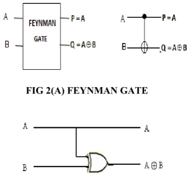
FEYNMAN GATE: The below figure (2) shows the logic circuit of Feynman 2×2 gate. Basically it is also known as controlled NOT gate (CNOT). This Feynmangate is used for the purpose of fan out characteristics and the quantum cost of this gate is equal to one. The input vector of Feynman gate is given as I (A, B) and in the same way the output vector is given as O (P, Q).
PERES GATE: The below figure shows (3) the logic circuit of peres3×3 gate. This peres gate realizes the various Boolean functions such as AND, XOR. The quantum cost of this gate is equal to four. The input vector of peres gate is given as I (A, B, C) and in the same way the output vector is given as O (P, Q, R).
FIG. 1. FREDKIN GATE (A) BLOCK DIAGRAM (B) QUANTUM REALIZATION (COST 5) FEYNMAN
DOUBLE GATE (C) BLOCK DIAGRAM (D) QUANTUM REALIZATION (COST 2).
FIG 2(A) FEYNMAN GATE
FREDKIN GATE: The below figure(4) shows the logic circuit of fredkin3×3 gate. The fredkin gate is used to implement a multiplexer. The quantum cost of this gate is equal to five. The input vector of fredkin gate is given as I (A, B, C) and in the same way the output vector is given as O (P, Q, R).
DKG GATE: The below figure (5) shows the logic circuit of 4×4 DKG gate. The main purpose of the DKG gate is that it produces large number of logical calculations. From figure we can see the output calculations. The input vector of DKG gate is given as I (A,B,C,D) and in the same way the output vector is given as O(P,Q,R,S).
IV. PROPOSED SYSTEM
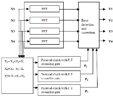
The below figure (6) shows the proposed architecture. In The proposed architecture we use FFTs, parsevals check with fault tolerance reversible gates and error correction and detection elements. The main intent of using this architecture is to reduce the number of SOC checks that are needed. In this architecture we are using praseval check with fault tolerant reversible gates for detecting errors. Along with that the number of FFTs is initiated in this architecture.
Here in this the both error detection and correction process are involved. But the error detection will use the ECC scheme in the same FIG. 3(A). PERES GATE
FIG .3(B) CIRCUIT DIAGRAM OF 3X3 PERES GATE
FIG .4(A) FREDKIN GATE
FIG .4(B) CIRCUIT DIAGRAM OF 3X3 FREDKINGATE
FIG. 5. DKG GATE
way the correction process uses parity- SOC – ECC technique. Here in the parity FFTs error will have no effect and does not propagate to the data outputs and in the same way it does not trigger any corrections. Coming to ECC, it is used for protection of elements and in the same way it detects all the errors. It propagates errors through the output. At last we can conclude that by using this proposed architecture we can detect and correct the errors. The below figure (7) shows the flow graph of radix-2 pipeline architecture. From this flow graph we can perform faster operation compared to existed system. As shown in figure (7), first an eight bit data is given to the radix-2 butterfly. This radix-2 butterfly blocks are connected to each other for better communication. The each block produces an individual output which are given as N/2, N/4 and N/8. At last we can conclude that the proposed system gives an flow graph by using radix-2 pipeline architecture for faster operation.
V. RESULTS
VI. CONCLUSION
In this paper we have discussed about the reversible gate of fault tolerant method. The main intent of this fault tolerant is to detect errors. To speed up the process we used fast Fourier transform and for logical calculations we used Perceval checks with fault tolerant reversible gate. At first in existed system there are no proper operation involved and errors are not correctly detected so to overcome we use parsevals check fault tolerant reversible gate. By using this we can detect the errors and correct it. So the proposed system gives better results like in terms of gates there is an increment of maximum value. There is not only increment in gates but also there is an increment in terms of quantum cost and unit delay which are given maximum to gates value.
VII. REFERENCES
[1] R. Landauer,“Irreversibility and heat generation in the computing process.” IBM J. Res.
Dev., vol.5,no. 3, pp. 183-191, 1961.
[2] C.H. Bennett,“Logical reversibility of computation”. IBM J. Res. Dev., vol.17, no. 6, pp. 525-532, 1973.
[3] Md. Shamsujjoha, H.M.H. Babu, L.Jamal, “Design of a compact reversible fault tolerant field programmable gate array: A novel approach in reversible logic synthesis”, Microelectron J., 2013 [4] A.S.M. Sayem, M.M.A. Polash, H.M.H. Babu, “Design of a reversible logic block of field
programmable gate array”, Silver
JubileeConferenceonCommunicationTechnologies
and VLSI Design, VIT University, Vellore,India, 2009.
FIG. 8. INPUT DATA
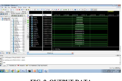
FIG. 9. OUTPUT DATA
[5]. C.H. Bennett. 1973. Logical reversibility of Computation, IBM Journal Research and Development. 17, 525-532.
[6] R. Landauer. 1961. Irreversibility and Heat Generation in the Computing Process. IBM Journal of Research and Development, 5(3), 183-191.
TELAPROLU KRISHNA MANOJ
completed his B.Tech at
Narasaraopeta Institute of
Technology and pursuing M.Tech at
Sri Chundi Ranganayakulu
Engineering College-JNTUK, India. His area of interest is VLSI.
Mr. MD.NAYEEMUDDIN received the B.Tech-ECE from JNTUK-Kakinada, India, in 2010 and
M.Tech-DECS from
JNTUK-Kakinada, India, in 2013. He is currently working as Assistant
Professor in Sri Chundi
Ranganayakulu Engineering
College-JNTUK, India. He has been active in research for more than 05 years and published 07 Journals in the field of Communications. He is a Life Member in Indian Society of research & development (ISRD) and
International Association of
Engineers (IAENG). His research interests include Antennas, VLSI, Embedded Systems, Mobile Cellular
Systems, and Digital Image