29
International Journal of Innovative and Emerging
Research in Engineering
e-ISSN: 2394 - 3343 p-ISSN: 2394 - 5494
Edge Detection Using Canny Algorithm on FPGA
Ms. AASIYA ANJUM1
a, Mr. SANJAY ASUTKAR2
b aAffiliation 1, Department of Electronic and telecommunication, Address, Dr, Shelkh bunker colony kamptee City, Nagpur and Country ,India
bAffiliation 2, Department of Electronic and telecommunication, City, Nagpur and Country, India
ABSTRACT:
In image processing and object recognition edge detection is used as a key stage. The Canny edge detection algorithm is used mostly because of its good performance. In this paper we present a edge detection using Canny algorithm on FPGA that results in significantly decrease Latency, decrease delay and increased throughput with no loss in edge detection. FPGA hardware architecture, Xilinx 13.1 software are used in this paper. The algorithm uses a low complexity 8 bit non-uniform gradient magnitude histogram to compute block based hysteresis thresholds that are used by the canny edge detector .The FPGA simulation results show that we can process a 218X218 image in 0.25msec at a clock rate of 100 MHz.
Keywords: Canny edge detector, FPGA , Distributed processing , Non uniform quantization
I. INTRODUCTION
Canny edge detection algorithm is used in real world application. Software are using for the implementation of edge detection algorithm. Edge detection serves as a first step for many image processing algorithm just like tracking, image enhancement, image/video coding and edge segmentation. Very large scale integration technology is used in this paper. Feild programmable gate array (FPGA) architecture is also using in this paper. Their hardware implementation has become as attractive especially for real time application. Good detection and good localization performance abilities are present in the canny edge detection algorithm thats why it is used in real world application. Unfortunetly preprocessing and post processing steps are coantains he anny edge detection algorithm and is more computationally complex than other edge detection algorithm such as oberts, Prewitt and Sobel algorithm.
In [4], we proposed a new threshold selection algorithm based on the distribution of pixel gradients in a block of ixels to overcome the dependency between the blocks. However, in [4], the hysteresis thresholds calculation is based on a very finely and uniformly quantized 64-bin gradient magnitude histogram, which is computationally xpensive and, thereby, hinders the real-time implementation. In this paper, a method based on non-uniform and coarse quantization of the gradient magnitude histogram is proposed.
II. CANNYEDGEDETECTIONALGORITHM
Canny developed an approach to derive an optimal edge detector based on three criteria related to the detection Performances
Volume 2, Issue 5, 2015
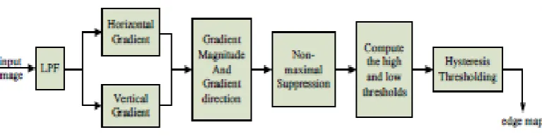
30 A block diagram of the Canny edge detection algorithm is shown in Fig. 1. The original Canny algorithm [5] consists of the following steps:
1. Smoothing the input image by Gaussian mask. The output smoothed image is denoted as I(x, y).
2. Calculating the horizontal gradient Gx(x, y) and vertical gradient Gy(x, y) at each pixel location by convolving the image I(x, y) with partial derivatives of a 2D Gaussian function.
3. Computing the gradient magnitude G(x, y) and direction θG(x, y) at each pixel location. 4. Applying non-maximum suppression (NMS) to thin edges.
5. Computing the hysteresis high and low thresholds based on the histogram of the magnitudes of the gradients of the entire image.
6. Performing hysteresis thresholding to determine the edge map.
III. PROPOSEDDISTRIBUTEDCANNYEDGEDETECTIONALGORITHM
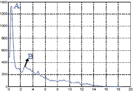
Canny edge detection algorithm has latency is propotional to the size of image because the canny edge detection algorithm operates on the whole image. Step 5, which is the hysteresis high and low thresholds calculation, is modified to enable parallel processing. In [4], a parallel hysteresis thresholding algorithm was proposed based on the observation that a pixel with a gradient magnitude of 2, 4 and 6 corresponds to blurred edges
Fig. 2(a) Original 512×512 House image
31 In this section, we describe the hardware implementation of our proposed distributed Canny edge detection algorithm on the Xilinx Spartan-3E FPGA.
A. Architecture Overview
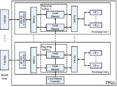
Fig. 3 The architecture of the proposed distributed Canny
SRAM memory and local memory are present in FPGA figure , in this figure CE is also presentt CE means compute engine The data bus width, the address bus width and the maximum system clock of the SRAM.
. Fig. 4 compute engine(CE) for the proposed
B. Image Smoothening
Volume 2, Issue 5, 2015
32
5(a) 5(b)
Fig. 5(a) Mask for the low pass Gaussian filter (b) Pipelined Image Smoothening Unit.
This architecture consist of Block RAM (BRAM)and 1-D finite impulse filter (FIR) .1-D finite impulse filter is used to process the data and Block RAM (BRAM)is used to store the data.
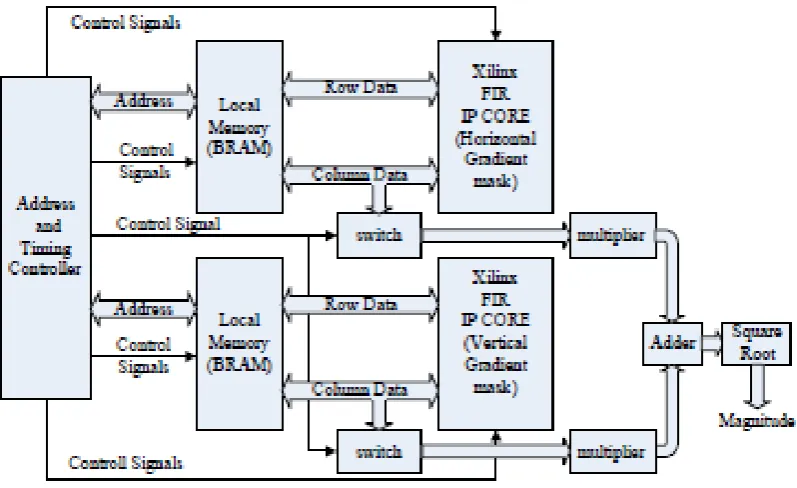
C. Gradients and Gradient Magnitude Calculation
Gradient and Gradient calculation is perform in this figureThis stage calculates the vertical and horizontal gradients using convolution kernels. The kernels vary in size from 3×3 to 9×9, depending on the harpness of the image. The Xilinx FIR core, which can support up to 256 Sets of coefficients with 2 to 1024 coefficient per set, is used to implement the kernals..
33 D. Directional Non Maximum Suppression
Fig.7 shows the architecture of the directional NMS unit. In order to access all the pixels’ gradient magnitudes in the 3×3 window at the same time, two FIFO buffers are employed.
Fig. 7.Directional Non Maximum Suppression Unit
Fig. 8 The architecture of the Threshold Calculation Unit.
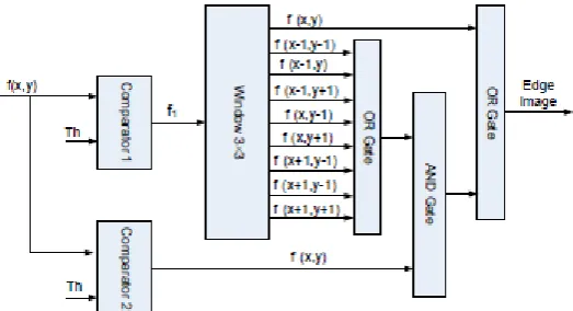
F. Thresholding with hysteresis
The method of hysteresis is used , the output of non maximum supperession is given to the thersholdind and hysteresis block.Two thresholds high and low are used.
Volume 2, Issue 5, 2015
34 V. SIMULATION RESULTS
A . Fixed-point Mat lab and FPGA Simulation Results
Fig.10(a) Edge map of Mat lab implementation;10{b) Edge map of FPGA implementation
Fig 11(a) The image after a 5X5 Gaussion mask has been passed across each pixel
35 VI. CONCLUSION
We present an Edge detection using Canny algorithm on FPGA that results in a significant speed up without Sacrificing the edge detection performance. As a result, the computational cost of the proposed algorithm is very low compared to the original Canny edge detection algorithm. Xilins 13.1 and Model sim software are used.. The minimum time period is 5.803ns and maximum frequency is 172.319MHz.. Number of BRAM 2 is used available12and utilization is 16%.
. REFERENCES
[1] F. M. Alzahrani and T. Chen, “A real-time edge detector algorithm and VLSI architecture,” Real-Time Imaging , vol. 3, no. 5, pp. 363 – 78, 1997.
[2] L. Torres, M. Robert, E. Bourennane, and M. Paindavoine ,“I implementation of a recursive real time edge detector using retiming techniques,” VLSI, pp. 811 –816,Aug. 1995.
[3] D. V. Rao and M. Venkatesan, “An efficient reconfigurable architecture and implementation of edge detection algorithm using Handle-C,” ITCC, vol. 2, pp. 843 – 847,Apr. 2004.
[4] S. Varadarajan, C. Chakrabarti, L. J. Karma, and J. M.Bauza , “A distributed psycho-visually motivated Canny edge detector,” IEEE ICASSP, pp. 822 –825, Mar. 2010.
[5] J. Canny, “A computational approach to edge detection,”IEEE Trans. PAMI, vol. 8, no. 6, pp. 679 –698, Nov. 1986.