ISSN (Online): 2348 – 3539.
Design and Analysis of Novel Current Mirror Circuit based
Level Shifter
1
Majida M.A,
2Yamuna.J
1PG Scholar, Department of Electronics and Communication Engineering, Dhanalakshmi Srinivasan College of
Engineering, Coimbatore.
2Assistant Professor, Department of Electronics and Communication Engineering, Dhanalakshmi Srinivasan
College of Engineering, Coimbatore. (ADR)
Abstract: Demand of handheld device like cellular phones, multimedia devices etc. are increasing and we are approaching towards portable device having small size which requires large battery life. But power dissipation has become most important design concern for VLSI circuits and system in low power devices. Level shifter is an interfacing circuit which can interface low core voltage to high input-output voltage. It can be either low voltage level or high voltage level. The level shifter allows communication between different modules without adding up any extra supply pin.This level shifter circuits are uses current mirror and the cross coupled based PMOS and N-MOS circuits. Here we are going to design the Wilson current mirror circuit and buffer based level shifter. For the further improvement of power and the delay we are going to design the novel current mirror circuits such as regulated cascade, large output swing current mirror based level shifter. By the improvement of transistor size we are going to design the pass transistor logic based Buffer circuit. These circuits are designed and verified by using the TANNER EDA tools.
Keywords: Wilson current mirror, PTL based buffer, voltage swing.
Reference to this paper should be made as follows: 1Majida M.A, 2Yamuna.J (2015) „Design and Analysis of Novel Current Mirror Circuit based Level Shifter‟, International Journal of Inventions in Computer Science and Engineering, Volume 2 Issue 4 2015.
1 Introduction
The real time observation systems that we tend to ordinarily stumble upon like hearing aids, pace makers [3] electrocardiograms etc need immoderate low power for extended life applications. Maintaining offer voltage below the brink voltage of the device ends up in reduced [2] power consumption [1]. But this ends up in enhanced delay of process. Hence level converters are needed to interface sub threshold [8] circuit voltage to core voltage level. Numerous level converters are on the market [5] for interface works. However threshold converters dissent from typical ones within the sense that, in typical ones massive voltage distinction between native provides exists.
Sub-threshold operation provides the bottom [12] energy per operation compared to ancient higher offer voltages [7] for applications in each general and reconfigurable physical science. However, this inflated energy efficiency [11] comes at the worth of a considerable degradation of performance. By extending the construct to voltage island methodologies, [7] that became wide in recent years, circuits will like the low power [5] aspects of sub-threshold operation by running the overwhelming majority [8] of the non-critical circuits at lower voltage than the high performance circuits – notably for reconfigurable circuits
that embrace peripheral [10] circuits requiring higher supply voltages.
same time. This paper deals with a low-power Level shifter implementation using [4] current mirror technique designed to convert near-threshold or sub-threshold voltages to above-threshold voltage levels. The fundamental strategy of current mirror is to supply 2 power modes a standby mode and a full of life mode.
II. Wilson Current Mirror
Current mirrors square measure basic building blocks utilized in electronic circuit styles of nowadays. A good variety of integrated circuits square measure supported current mirrors (even there square measure whole op-amps created solely by current mirrors). There's style of current mirror circuits; Wilson current mirror is one amongst the foremost standard of them. Though this clever circuit consists solely of three transistors (Fig. 1) it's too tough to grasp what the fundamental plan behind it‟s and the way it operates because it's explained sometimes by formal implies that do not reveal the foundation of the matter.
Figure-1 shows the Wilson Current Mirror circuit victimization NMOS transistors as active components. The semiconductor M1 is connected, forcing its Drain to Gate voltage to zero [1]. During this mode semiconductor M1 operates within the saturation region that in turns acts as a relentless current supply or reference current supply. To figure as a current mirror, each M1 and M2 square measure chosen to be identical MOS transistors. Neglecting the channel length modulation result, if the gate source of M3 is being biased to a hard and fast voltage produces a duplicate of reference current.
A.
Wide Range Level Shifter Using Wilson
Current Mirror Circuit
A Wilson current mirror or Wilson current source is a circuit configuration designed to provide a constant current. This circuit has the advantage of virtually eliminating the current mismatch of the conventional current mirror thereby ensuring that the output current is almost equal to the reference or input current thus eliminating the drawbacks of cascade structure.The needs for 2 voltage offer limit the physical placement of such level shifter to the boundary of high and low voltage styles that restricts the physical style
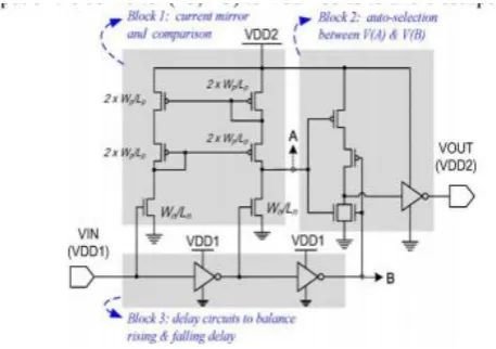
needs just one offer VddH to convert the low Voltage signal to the upper voltage has been proposed. It makes the position way more versatile within the entire high voltage regions. Figure 2 shows the schematic diagram of Wilson current mirror based level shifter. The brink drop (VDD1) across the NMOS provides a virtual VddL to the input electrical converter (P2, N2). The output stage may be a 0.5 latch that pulls up the input of the converter (P3, N3) to VddH so as to avoid escape.
Once sign (in) is HIGH, the voltage at node A is (VddH) with the aim of reducing gate to supply voltage of P2 to show it OFF. Once the sign (in) is LOW, the auto selection node activates so charges node A to B for compensate the brink drop. Hence the availability voltage of converter (A-B) is dynamically switched between Vdd1 and Vdd2 relying upon the input state.
III. Self Cascode Current Mirror Circuit
This circuit consists of 4 NMOS transistors as M1, M2, M3 and M4. The modified circuit can also to be adopted for the input supply to the output voltage. The reference can be possible to layer out from the desired coupling of buffer and the input stages for auto selection of A and B nodes and also easy to get the final level output as VDD2.
B.
Self Cascode based Level Shifter
Self cascade current mirror with buffer stages can complete the level shifter circuit for converter applications. This could be adopted for low power and the delay based circuits for the implementation of all the perfromance representation in the blocks
.
The inverter stages for the delay could be processed for two stages and also can be detailed for the auto selection stages from the VDD1 to the VDD2. The sectional and the architecture view can be adopted for the high output gain from this circuit.
IV. Regulated Cascade Current Mirror Based
Level Shifter
A regulated cascade structure behaves sort of a MOS semiconductor with higher output and improved frequency response. Figure 5 shows current mirror created by utilizing transistor like „regulated cascade structure.
Although, this structure offers improved characteristics attributable to matching of drive transistors, it doesn't modification the input and output compliance voltage, so stop low voltage operation. A solution to the current drawback is provided in that enhance the input signal swing capability additionally to adaptive biasing to facilitate low voltage operation.
The drive semiconductor device M1 converts the input voltage into a drain current that flows through the drain-source path of money supply to the output terminal. To mitigate the result of channel length modulation of M1, its drain-source voltage should be maintained at fastened voltage level. This could be accomplished by a feedback circuit consisting of Associate in electronic equipment and money supply as supply follower, thereby increasing the output resistance.
C.
Regulated Cascade Level Shifter
NMOS transistor with the reduced power and the delay based parameters for the further improvement of level shifter applications. These stages can be adopted for the supply voltages for standard and the sub-threshold ranges. Then the VDD2 get the standard supply voltages for the singular and the dual voltage level shifters.
Level Shifter with PTL based Buffer
Pass Transistor Logic (PTL) is a well known approach for implementing digital circuit. This implementation could be used in this level shifter for the reduced power and the delay based parameters. This circuit used in all mirror circuit with the inverter stages for the improvement of sectional and the architectural view. The wide spreading application can be added as a signal view for the generation of the voltage levels from the VDD1 to VDD2.
Full Range Level Shifter
A full range of level shifter with multiplexer has been designed and verified using the modified level shifte ranges into the output selection. This could be used as a commucation level synthesis for the further most implementation. The sectional view from this application may be converted as a signal generator for the full range of applications.
Level shifter1 and Level shifter 2 could be a modified and the proposed level shifters. The multiplexer could be used and then the selection lines are selected from which range could be used for the all applications.
V. Simulation Results
VI. Conclusion
The growth in energy-scavenging and battery high-powered electronics has initiated a revolution in ultra-low power chips style. New applications area unit rising which will require at the same time increasing levels of energy efficiency with intermittent needs for top performance also included. A clear optimization for these physics is to use multiple provide voltages to attenuate power consumption. Taking this approach to the intense includes operating most of the circuits at ultra-low sub-threshold voltage levels; but, translating the ensuing digital signals between totally different voltage domains remains a challenge.
In this report, many level shifters are evaluated in the context of translating signals from sub-threshold levels to ancient CMOS levels. 3 standard circuits were enclosed within the analysis also as 3 novel level shifters planned for the primary time during this paper. All six circuits were evaluated in terms of power, performance and radiation hardness for a relentless space. Voltage doublers were eliminated from thought supported problems with delay and operational vary. The planned current mirror level shifter with dynamically-adjusted threshold was the best in terms of performance and power.
References
[1] M. Alioto, “Ultra-low power VLSI circuit design demystified and explained: A tutorial,” IEEE Trans. Circuits Syst. I, Reg. Papers, vol. 59, no. 1, pp. 3–29, Jan. 2012.
[2] T.-T. Liu and J. M. Rabaey, “A 0.25 V 460 nW asynchronous neural signal processor with inherent leakage suppression,” IEEE J. Solid- State Circuits, vol. 48, no. 4, pp. 897–906, Apr. 2013.
[3] Y. Zhang, F. Zhang, Y. Shakhsheer, J. D. Silver, A. Klinefelter, M. Nagaraju, J. Boley, J. Pandey, A.
P. Otis, “A batteryless 19 WMICS/ISM-band energy harvesting body sensor node SoC for ExG applications,” IEEE J. Solid-State Circuits, vol. 48, no. 1, pp. 199–213, Jan. 2013.
[4] T. Lin, K.-S. Chong, J. S. Chang, and B.-H. Gwee, “An ultra-low power asynchronous-logic insitu self-adaptive system for wireless sensor networks,” IEEE J. Solid-State Circuits, vol. 48, no. 2, pp. 573–586, Feb. 2013.
[5] S. Lütkemeier, T. Jungeblut, H. K. O. Berge, S. Aunet, M. Porrmann, and U. Rückert, “A 65 nm 32 b subthreshold processor with 9T multi-Vt SRAM and adaptive supply voltage control,” IEEE J. Solid-State Circuits, vol. 48, no. 1, pp. 8–19, Jan. 2013.
[6] S. Hsu, A. Agarwal, M. Anders, S. Mathew, H. Kaul, F. Sheikh, and R. Krishnamurthy, “A 280 mV-to-1.1 V 256 b reconfigurable SIMD vector permutation engine with 2-dimensional shuffle in 22 nm CMOS,” in Proc. IEEE Int. Solid-State Circuits Conf. Dig. Tech. Papers (ISSCC), Feb. 2012, pp. 178–180.
[7] S. Lütkemeier and U. Rückert, “A subthreshold to above-threshold level shifter comprising a wilson current mirror,” IEEE Trans Circuits Syst. II, Exp. Briefs, vol. 57, no. 9, pp. 721–724, Sept. 2010.
[8] S. N. Wooters, B. H. Calhoun, and T. N. Blalock, “An energy-efficient subthreshold level converter in 130-nm CMOS,” IEEE Trans Circuits Syst. II, Exp. Briefs, vol. 57, no. 4, pp. 290–294, Apr. 2010.
[9] Y. Osaki, T. Hirose, N. Kuroki, and M. Numa, “A low-power level shifter with logic error correction for extremely low-voltage digital CMOS LSIs,” IEEE J. Solid-State Circuits, vol. 47, no. 7, pp. 1776–1783, July 2012.
[10] M. Lanuzza, P. Corsonello, and S. Perri, “Low-power level shifter for multi-supply voltage designs,” IEEE Trans Circuits Syst. II, Exp. Briefs, vol. 59, no. 12, pp. 922–926, Dec. 2012.
[11] M.-W. Chen, M.-H. Chang, Y.-H. , and W. Hwang, “An energy-efficient level converter with high thermal variation immunity for sub-threshold to super-threshold operation,” in Proc. IEEE Int. SOC Conf. (SOCC), Sept. 2012, pp. 5–10.
[12] A. Hasanbegovic and S. Aunet, “Low-power sub-threshold to above sub-threshold level shifter in 90 nm process,” in Proc. Conf. NORCHIP, 2009, pp. 1–4.