EC64 VLSI DESIGN SYLLABUS
UNIT I CMOS TECHNOLOGY
A brief History-MOS transistor, Ideal I-V characteristics, C-V characteristics, Non ideal IV effects, DC transfer characteristics - CMOS technologies, Layout design Rules, CMOS process enhancements, Technology related CAD issues, Manufacturing issues
UNIT II CIRCUIT CHARACTERIZATION AND SIMULATION
Delay estimation, Logical effort and Transistor sizing, Power dissipation, Interconnect, Design margin, Reliability, Scaling- SPICE tutorial, Device models, Device characterization, Circuit characterization, Interconnect simulation
UNIT III COMBINATIONAL AND SEQUENTIAL CIRCUIT DESIGN
Circuit families –Low power logic design – comparison of circuit families – Sequencing static circuits, circuit design of latches and flip flops, Static sequencing element methodology- sequencing dynamic circuits – synchronizers
UNIT IV CMOS TESTING
Need for testing- Testers, Text fixtures and test programs- Logic verification- Silicon debug principles- Manufacturing test – Design for testability – Boundary scan
UNIT V SPECIFICATION USING VERILOG HDL
Basic concepts- identifiers- gate primitives, gate delays, operators, timing controls, procedural assignments conditional statements, Data flow and RTL, structural gate level switch level modeling, Design hierarchies, Behavioral and RTL modeling, Test benches, Structural gate level description of decoder, equality detector, comparator, priority encoder, half adder, full adder, Ripple carry adder, D latch and D flip flop.
Textbooks:
1. Weste and Harris: CMOS VLSI DESIGN (Third edition) Pearson Education, 2005 2. Uyemura J.P: Introduction to VLSI circuits and systems, Wiley 2002.
3. J.Bhasker,”Verilog HDl Primer“ , BS publication,2001(UNIT V)
References:
1 D.A Pucknell & K.Eshraghian Basic VLSI Design, Third edition, PHI, 2003 2 Wayne Wolf, Modern VLSI design, Pearson Education, 2003
UNIT I CMOS TECHNOLOGY
INTRODUCTION
An MOS (Metal-Oxide-Silicon) structure is created by superimposing several layers of conducting, insulating, and transistor forming materials. After a series of processing steps, a typical structure might consists of levels called diffusion, polysilicon, and metal that are separated by insulating layers. CMOS technology provides two types of transistors, an n-type transistor (n MOS) and a p-type transistor (p MOS). These are fabricated in silicon by using either negatively doped silicon that is rich in electrons (negatively charged) or positively doped silicon that is rich in holes (the dual of electrons and positively charged). For the n-transistor, the structure consists of a section of p-type silicon separating two diffused areas of n-type silicon. The area separating the n regions is capped with a sandwich consisting of an insulator and a conducting electrode called the GATE. Similarly, for the p-transistor the structure consists of a section of n-type silicon separating two p-type diffused areas. The p-transistor also has a gate electrode. The gate is a control input and it affects the flow of electrical current between the drain and source. The drain and source may be viewed as two switched terminals.
CV Characteristics:
The measured MOS capacitance (called gate capacitance) varies with the applied gate voltage
– A very powerful diagnostic tool for identifying any deviations from the ideal in both
oxide and semiconductor
– Routinely monitored during MMOS device fabrication
Measurement of C-V characteristics
– Apply any dc bias, and superimpose a small (15 mV) ac signal
– Generally measured at 1 MHz (high frequency) or at variable frequencies between
1KHz to 1 MHz
– The dc bias VG is slowly varied to get quasi-continuous C-V characteristics
DC Characteristics of CMOS inverter
Ids = K W (Vds – Vt)Vds – Vds 2 L 2
Figure 2.3 CMOS inverter
In the resistive region, or
Ids = K W (Vgs – Vt)2 L 2
In the saturation region. In both cases the factor K is a technology- dependent parameter such that
K = εins εo µ
D
The factor W/L is contributed by the geometry and it is common practice to write β = K W
L Such that,
Ids = β (Vgs – Vt)2 2
In saturation, and where β may be applied to both nMOS and pMOS transistors as follows, βn = εins εo µn Wn
D Ln
βp = εins εo µp Wp
D Lp
Figure 2.4 Transfer characteristics
Considering the static condition first, in region 1 for which Vin = logic 0, the p-transistor fully turned on while the n-transistor is fully turned off. Thus no current flows through the inverter and the output is directly connected to VDD through the p-transistor.
In region 5 Vin = logic 1, the n-transistor is fully on while the p-transistor is fully off. Again, no current flows and a good logic 0 appears at the output.
In region 2 the input voltage has increased to a level which just exceeds the threshold voltage of the n-transistor. The n-transistor conducts and has a large voltage between source and drain. The p-transistor also conducting but with only a small voltage across it, it operates in the unsaturated resistive region.
In region 4 is similar to region 2 but with the roles of the p- and n- transistors reversed. The current magnitudes in region 2 and 4 are small and most of the energy consumed in switching from one state to the other is due to the large current which flows in region 3.
In region 3 is the region in which the inverter exhibits gain and in which both transistors are in saturation.
The currents in each device must be the same since the transistors are in series. So we may write
I dsp = - Idsn
Where
Idsp= βn (Vin – VDD - Vtp )2
2 And
Idsn = βn (Vin – Vtn )2 2
Vin in terms of the β ratio and the other circuit voltages and currents Vin = VDD + Vtp +Vtn (βn + βp)1/2
1+ (βn + βp)1/2
Since both transistors are in saturation, they act as current sources so that the equivalent circuit in this region is two current sources so that the equivalent circuit in this region is two current sources in series between VDD and VSS with the output voltage coming from their common point. The region is inherently unstable in consequence and the change over from one logic level to the other is rapid.
If βn= βp and if Vin = -Vtp, then
Vin = 0.5 VDD
Since only at this point will the two β factors be equal. But for βn= βp the device geometries must be
such that
µp Wp/Lp = µn Wn/Ln
The mobilities are inherently unequal and thus it is necessary for the width to length ratio of the p-device to be three times that of the n-p-device, namely
Wp/Lp = 2.5 Wn/Ln
The mobility µ is affected by the transverse electric field in the channel and is thus independent on Vgs. It has been shown empirically that the actual mobility is
µ = µz (1 – Ø (Vgs – Vt)-1
CMOS TECHNOLOGIES
CMOS provides an inherently low power static circuit technology that has the capability of providing a lower-delay product than comparable design-rule nMOS or pMOS technologies. The four dominant CMOS technologies are:
P-well process n-well process twin-tub process Silicon on chip process
The p-well process
A common approach to p-well CMOS fabrication is to start with moderately doped n-type substrate (wafer), create the p-type well for the n-channel devices, and build the p-channel transistor in the native n-substrate. The processing steps are,
1. The first mask defines the p-well (p-tub) n-channel transistors (Fig. 1.5a) will be fabricated in this well. Field oxide (FOX) is etched away to allow a deep diffusion.
2. The next mask is called the “thin oxide” or “thinox” mask (Fig. 1.5b), as it defines where areas of thin oxide are needed to implement transistor gates and allow implantation to form p- or n- type diffusions for transistor source/drain regions. The field oxide areas are etched to the silicon surface and then the thin oxide areas is grown on these areas. O ther terms for this mask include active area, island, and mesa.
3. Polysilicon gate definition is then completed. This involves covering the surface with polysilicon (Fig 1.5c) and then etching the required pattern (in this case an inverted “U”). “Poly” gate regions lead to “self-aligned” source-drain regions.
4. A p-plus (p+) mask is then used to indicate those thin-oxide areas (and polysilicon) that are to be implanted p+. Hence a thin-oxide area exposed by the p-plus mask (Fig. 1.5d) will become a p+ diffusion area. If the plus area is in the n-substrate, then a channel transistor or p-type wire may be constructed. If the p-plus area is in the p-well, then an ohmic contact to the p-well may be constructed.
5. The next step usually uses the complement of the p-plus mask, although an extra mask is normally not needed. The “absence” of a p-plus region over a thin-oxide area indicates that
n-transistors and wires. An n+ diffusion (Fig. 1.5e) in the n-substrate allows an ohmic contact to be made. Following this step, the surface of the chip is covered with a layer of Sio2.
6. Contacts cuts are then defined. This involves etching any Sio2 down to the contacted surface, these allow metal (Fig. 1.5f) to contact diffusion regions or polysilicon regions.
7. Metallization (Fig. 1.5g) is then applied to the surface and selectively etched.
8. As a final step, the wafer is passivated and openings to the bond pads are etched to allow for wire bonding. Passivation protects the silicon surface against the ingress of contaminants.
(a)
(b)
(d)
(e)
(f)
(g)
Basically the structure consists of an n-type substrate in which p-devices may be formed by suitable masking and diffusion and, in order to accommodate n-type devices, a deep p-well is diffused into the n-type substrate. This diffusion must be carried out with special care since the p-well doping concentration and depth will affect the threshold voltages as well as the breakdown voltages of the n-transistors. To achieve low threshold voltage (0.6 to 1.0 V), deep well diffusion or high well resistivity is needed. However, deep wells require larger spacing between the n- and p-type transistors and wires because of lateral diffusion resulting in larger chip areas.
High resistivity can accentuate latch-up problems. In order to achieve narrow threshold voltage tolerances in a typical p-well process, the well concentration is made about one order of magnitude higher than the substrate doping density, thereby causing the body effect for n-channel devices to be higher than for p-channel transistors. In addition, due to this higher concentration, n-transistors suffer from excessive source/drain to p-well capacitance will tends to be slower in performance. The well must be grounded in such a way as to minimize any voltage drop due to injected current in substrate that is collected by the p-well.
The p-well act as substrate for then-devices within the parent n-substrate, and, provided polarity restrictions are observed, the two areas are electrically isolated such that there are in affect two substrate, two substrate connections (VDD and VSS) are required.
The n-well process:
The p-well processes have been one of the most commonly available forms of CMOS. However, an advantage of the n-well process is that it can be fabricated on the same process line as conventional n MOS. n –well CMOS circuits are also superior to p-well because of the lower substrate bias effects on transistor threshold voltage and inherently lower parasitic capacitances associated with source and drain regions.
Figure 1.6 Main steps in a typical n-well process
Due to differences in mobility of charge carriers the n-well process creates non-optimum p-channel characteristics, such as high junction capacitance and high body effect. The n-well technology has a distinct advantage of providing optimum device characteristics. Thus n-channel devices may be used to form logic elements to provide speed and density, while p-transistors could primarily serve as pull-up devices.
The twin-tub process:
Twin-tub CMOS technology provides the basis for separate optimization of the p-type and n-type transistors, thus making it possible for threshold voltage, body effect, and the gain associated with n-and p-devices to be independently optimized. Generally the starting material is either an n+ or p+ substrate with a lightly doped epitaxial or epi layer, which is used for protection against latch-up. The aim of epitaxy is to grow high purity silicon layers of controlled thickness with accurately determined dopant concentrations distributed homogeneously throughout the layer. The electrical properties for this layer are determined by the dopant and its concentration in the silicon.
The process sequence, which is similar to the p-well process apart from the tub formation where both p-well and n-well are utilized as in Fig. 1.7, entails the following steps:
Thin oxide etching
Source and drain implantations Contact cut definition
Metallization.
Since this process provides separately optimized wells, better performance n-transistors (lower capacitance, less body effect) may be constructed when compared with a conventional p-well process. Similarly the p-transistors may be optimized. The use of threshold adjust steps is included in this process.
Silicon on insulator process:
Silicon on insulator (SOI) CMOS processes has several potential advantages such as higher density, no latch-up problems, and lower parasitic capacitances. In the SOI process a thin layer of single crystal silicon film is epitaxial grown on an insulator such as sapphire or magnesium aluminate spinel. The steps involves are:
1) A thin film (7-8 µm) of very lightly doped n-type Si is grown over an insulator (Fig. 1.8a). Sapphire is a commonly used insulator.
2) An anisotropic etch is used to etch away the Si (Fig. 1.8b) except where a diffusion area will be needed.
3) The p-islands are formed next by masking the n-islands with a photoresist. A p-type dopant (boron) is then implanted. It is masked by the photoresist and at the unmasked islands. The p-islands (Fig. 1.8c) will become the n-channel devices.
4) The p-islands are then covered with a photoresist and an n-type dopant, phosphorus, is implanted to form the n-islands (Fig. 1.8d). The n-islands will become the p-channel devices.
5) A thin gate oxide (500-600Å) is grown over all of the Si structures (Fig. 1.8e). This is normally done by thermal oxidation.
6) A polysilicon film is deposited over the oxide.
7) The polysilicon is then patterned by photomasking and is etched. This defines the polysilicon layer in the structure as in Fig. 1.8f.
8) The next step is to form the n-doped source and drain of the n-channel devices in the p-islands. The n-island is covered with a photoresist and an n-type dopant (phosphorus) is implanted (Fig. 1.8g).
10) A layer of phosphorus glass is deposited over the entire structure. The glass is etched at contact cut locations. The metallization layer is formed. A final passivation layer of a phosphorus glass is deposited and etched over bonding pad locations.
(a)
(b)
(c)
( d )
(e)
(f)
(h)
Figure 1.8 SOI fabrication steps
The advantages of SOI technology are:
Due to the absence of wells, denser structures than bulk silicon can be obtained.
Low capacitances provide the basis of very fast circuits.
No field-inversion problems exist.
No latch-up due to isolation of n- and p- transistors by insulating substrate.
As there is no conducting substrate, there are no body effect problems
Enhanced radiation tolerance.
But the drawback is due to absence of substrate diodes, the inputs are difficult to protect. As device gains are lower, I/O structures have to be larger. Single crystal sapphires are more expensive than silicon and processing techniques tend to be less developed than bulk silicon techniques.
BiCMOS TECHNOLOGY FABRICATION
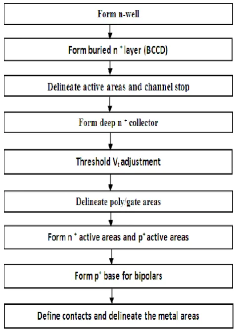
The production of npn bipolar transistors with good performance characteristics can be achieved by extending the standard n-well CMOS processing to include further masks to add two additional layers such as the n+ subcollector and p+ base layers. The npn transistors is formed in an n-well and the additional p+ base region is located in the well to form the p-base region of the transistor. The second additional layer, the buried n+ subcollector (BCCD), is added to reduce the n-well (collector) resistance and thus improve the quality of the bipolar transistor. The arrangement of BiCMOS npn transistor is shown in Fig. 1.9.
Figure 1.9 Arrangement of BiCMOS npn transistor
UNIT II CIRCUIT CHARACTERIZATION AND SIMULATION
Delay estimation:
Estimation of the delay of a Boolean function from its functional description is an important step towards design exploration at the register transfer level (RTL). This paper addresses the problem of estimating the delay of certain optimal multi-level implementations of combinational circuits, given only their functional description. The proposed delay model uses a new complexity measure called the delay measure to estimate the delay. It has an advantage that it can be used to predict both, the minimum delay (associated with an optimum delay implementation) and the maximum delay (associated with an optimum area implementation) of a Boolean function without actually resorting to logic synthesis. The model is empirical and results demonstrating its feasibility and utility are presented.
tpdr: rising propagation delay
From input to rising output crossing VDD/2 tpdf: falling propagation delay
From input to falling output crossing VDD/2 tpd: average propagation delay
tpd = (tpdr + tpdf)/2 tr: rise time
From output crossing 20% to 80% VDD tf: fall time
From output crossing 80% to 20% VDD tcd: average contamination delay
tcd = (tcdr + tcdf)/2
tcdr: rising contamination delay: Min from input to rising output crossing VDD/2 tcdf: falling contamination delay: Min from input to falling output crossinVDD/2
Solving differential equations by hand is hard. SPICE like simulators used for accurate analysis. But simulations are expensive. We need to be able to estimate delay although not as accurately as simulator.
Use RC delay models to estimate delay
C = total capacitance on the output node Use Effective resistance R
Therefore tpd = RC
Transistor sizing:
Not all gates need to have the same delay.
Not all inputs to a gate need to have the same delay. Adjust transistor sizes to achieve desired delay.
Example: Adder carry chain
Inter-stage effects in transistor sizing
� Increasing a gate’s drive also increases the load to the previous stage
Logical effort
Logical effort is a gate delay model that takes transistor sizes into account. Allows us to optimize transistor sizes over combinational networks. Isn’t as accurate for circuits with reconvergent fanout.
Logical effort gate delay model
� Express delays in process-independent unit
� Gate delay is measured in units of minimum-size
inverter delay τ.
d = f + p.
� Effort delay f is related to gate’s load. Parasitic delay p depends on gate’s structure. Represents
delay of gate driving no load Set by internal parasitic capacitance Effort delay
� Effort delay has two components: f = gh.
� Electrical effort h is determined by gate’s load: h = Cout/Cin Sometimes called fanout
� Logical effort g is determined by gate’s structure. Measures relative ability of gate to deliver current g ≡ 1 for inverter
Delay plots:
Computing Logical Effort
� Logical effort is the ratio of the input capacitance of a gate to the input capacitance of an inverter
Power Estimation:
The past the major concerns of the VLSI designer were area performance cost and reliability power considerations were mostly of only secondary importance. In recent years however this has begun to change and increasingly power is being given comparable weight to area and speed. Several factors have contributed to this trend Perhaps the primary driving factor has been the remarkable success and growth of the class of personal computing devices portable desktops audio and videobased multimedia products_ and wireless communications systems _personal digital assistants and personal communicators_ which demand high_speed computation and complex functionality with In the past_ the major concerns of the VLSI designer were area_ performance cost and reliability_ power considerations were mostly of only secondary importance_ In recent years_ however_ this has begun to change and_ increasingly_ power is being given comparable weight to area and speed_ Several factors have contributed to this trend Perhaps the primary driving factor has been the remarkable success and growth of the class of personal computing devices _portable desktops_ audio_ and video_based multimedia products and wireless communications systems _personal digital assistants and personal communicators which demand high_speed computation and complex functionality with low power consumption_ There also exists a strong pressure for producers of high_end products to reduce their power consumption.
Software_Level Power Estimation
The first task in the estimation of power consumption of a digital system is to identify the typical application programs that will be executed on the system. A non_trivial application program consumes millions of machine cycles_ making it nearly impossible to perform power estimation using the complete program at_ say_ the RT_level_ Most of the reported results are based on power macro_modeling_ an estimation approach which is extensively used for behavioral and RTL level estimation see Sections and In the power cost of a CPU module is characterized by estimating the average capacitance that would switch when the given CPU module is activated_In the switching activities on _address_ instruction_ and data_ buses are used to estimate the power consumption of the microprocessor, based on actual current measurements of some processors_ Tiwari et al_ present the following instruction_level power model
synthesis_ to perform RT_level power estimation for high performance CPUs_ Instead of using a macro_modeling equation to model the energy dissipation of a microprocessor_ the authors use a synthesized program to exercise the microprocessor in such a way that the resulting instruction trace behaves _in terms of performance and power dissipation_ much the same as the original trace_ The new instruction trace is however much shorter than the original one_ and can hence be simulated on a RT_level description of the target microprocessor to provide the power dissipation results quickly_ Specifically_ this approach consists of the following steps_
Perform architectural simulation of the target microprocessor under the instruction trace of
typical application programs_
Extract a characteristic pro_le_ including parameters such as the instruction mix_ Instruction
data cache miss rates_ branch prediction miss rate_ pipeline stalls_ etc_ for the microprocessor.
Use mixed integer linear programming and heuristic rules to gradually transform a generic
program template into a fully functional program_
Perform RT_level simulation of the target microprocessor under the instruction trace of the
new synthesized program _
Notice that the performance of the architectural simulator in gate vectors second is roughly to orders of magnitude higher than that of a RT_level simulator. This approach has been applied to the Intel Pentium processor _which is a super_ scalar pipelined CPU with _KB _way set_associative data_ instruction and data caches_ branch prediction and dual instruction pipeline_ demonstrating _ to _ orders of magnitude reduction in the RT_level simulation time with negligible estimation error. Behavioral_Level Power Estimation
Conversely from some of the RT_level methods that will be discussed in Section estimation techniques at the behavioral_level cannot rely on information about the gatelevel structure of the design components_ and hence_ must resort to abstract notions of physical capacitance and switching activity to predict power dissipation in the design_
Information_Theoretic Models
Information theoretic approaches for high_level power estimation depend on information theoretic measures of activity .for example_ entropy_ to obtain quick power estimates Entropy characterizes the randomness or uncertainty of a sequence of applied vectors and thus is intuitively related to switching activity_ that is_ if the signal switching is high_ it is likely that the bit sequence is random_ resulting in high entropy_ Suppose the sequence contains t distinct vectors and let pi denote the occurrence probability of any vector v in the sequence_ Obviously_
where log x denotes the base logarithm of x_ The entropy achieves its maximum value of log t when pi log pi For an n_bit vector(t,n)his makes the computation of the exact entropy very expensive. Assuming that the individual bits in the vector are independent_ then we can write
where qi denotes the signal probability of bit i in the vector sequence. Note that this equation is only an upperbound on the exact entropy, since the bits may be dependent. This upperbound expression is_ however_ the one that is used for power estimation purposes. Furthermore in it has been shown that_ under the temporal independence assumption_ the average switching activity of a bit is upper_bounded by one half of its entropy
The power dissipation in the circuit can be approximated as
Where Ctot is the total capacitance of the logic module including gate and interconnect capacitances_ and Eavg is the average activity of each line in the circuit which is inturn approximated by one half of its average entropy havg. The average line entropy is computed by abstracting information obtained from a gate_level implementation. In it is assumed that the word_level entropy per logic level reduces quadratically from circuit inputs to circuit outputs_ whereas in it is assumed that the bit_level entropy from one logic level to next decreases in an exponential manner. Based on these assumptions two different computational models are obtained
In Marculescu et al_ derive a closed_form expression for the average line entropy for the case of a linear gate distribution(i.e.,)when the number of nodes scales linearly between the number of circuit inputs n and circuit outputs m. The expression for havg is given by
where hin and hout denote the average bit_level entropies of circuit inputs and outputs_respectively_ hin is extracted from the given input sequence_ whereas hout is calculated from a quick functional simulation of the circuit under the given input sequence or by empirical entropy propagation techniques for pre_characterized library modules. In Nemani and Najm propose the following expression for havg
they are approximated as the summation of individual bit_level entropies_ hin and hout. If the circuit structure is given_ the total module capacitance is calculated by traversing the circuit netlist and summing up the gate loadings_ Wire capacitances are estimated using statistical wire load models_ Otherwise_ Ctot is estimated by quick mapping for example_ mapping to __input universal gates_ or by information theoretic models that relate the gate complexity of a design to the di_erence of its input and output entropies. One such model proposed by Cheng and Agrawal in for example estimates
This estimate tends to be too pessimistic when n is large hence in Ferrandi et al_ present a new total capacitance estimate based on the number N of nodes i.e.,to multiplexors in the Ordered Binary Decision Diagrams OBDD representation of the logic circuit as follows
The coefficients of the model are obtained empirically by doing linear regression analysis on the total capacitance values for a large number of synthesized circuits. Entropic models for the controller circuitry are proposed by Tyagi in where three entropic lower bounds on the average Hamming distance _bit changes_ with state set S and with T states_ are provided. The tightest lower bound derived in this paper for a sparse _nite state machine FSM i.e., tT log T where t is the total number of transitions with nonzero steady_state probability_ is the following
where pi,j is the steady state transition probability from si to sj H(si,sj) is the Hamming distance between the two states_ and h(pi,j) is the entropy of the probability distribution pi,j . Notice that the lower bound is valid regardless of the state encoding used. In using a Markov chain model for the behavior of the states of the FSM_ the authors derive theoretical lower and upper bounds for the average Hamming distance on the state lines which are valid irrespective of the state encoding used in the final implementation. Experimental results obtained for the mcnc benchmark suite show that these bounds are tighter than the bounds reported.
Design Margin:
nowadays. This paper investigates the effects of corner relaxation on overall circuit performance metrics (yield, power, area) at the gate/transistor levels. Experimental results indicate that if we design the circuit using relaxed corner, though the circuit yield is somewhat reduced, we can get some advantages in area and power aspects.
Reliability:
Yield and reliability are two of the cornerstones of a successful IC manufacturing technology along with product performance and cost. Many factors contribute to the achievement of high yield and reliability, and many of these also interact with product performance and cost. A fundamental understanding of failure mechanisms and yield limitations enables the up-front achievement of these technology goals through circuit and layout design, device design, materials choices, process optimization, and thermo-mechanical considerations. Failure isolation and analysis, defect analysis, low yield analysis, and materials analysis are critical methodologies for the improvement of yield and reliability. Coordination of people in many disciplines is needed in order to achieve high yield and reliability. Each needs to understand the impact of their choices and methods on the final product. Unfortunately, very little formal university training exists in these critical areas of IC reliability, yield, and failure analysis.
Reliability Fundamentals and Scaling Principles
The Reliability Bathtub Curve, Its Origin and Implications Key Reliability Functions and Their Use in Reliability Analysis Defect Screening Techniques and Their Effectiveness
Accelerated Testing and Estimation of Useful Operating Life Reliability Data Collection and Analysis in Integrated Circuits Past Technology Scaling Trends
Forward Looking Projections with a Focus on Examining and Understanding of the Impact on
VLSI Reliability
Power Density Trends: Operating temperature, activation energies for dominant vlsi failure
mechanisms, and reliability impact
Reliability Strategies In Fabless Environments
Reliability of the Interconnect System
Mechanical Stress Driven Metal Voiding and Cracking
Low k Materials as Interlayer Dielectrics and Their Impact on Electro-migration Thermo-mechanical Integrity of the Interconnect System
Key Technology Parameters: Materials choices, structural and geometric effects Extreme Scaling Impact on Wear-out Time
Technology Solutions: Alloys, metal barriers, and engineering of interfaces Improved Electro-migration Performance under Non-DC Currents and Short Lines Interconnect Reliability Strategies in Fabless Environments
Transistor Reliability: Dielectric Breakdown, Hot Carriers and Parametric Stability
Physics, Statistics, and Scaling Impact on Failure Mechanisms
Reliability Performance of Thin Conventional Oxides: Defects, wear-out failures
Hot Carrier Performance and Parametric Stability of P- and N-channel Devices under DC and
AC
High k Gate Dielectrics and Novel Transistor Configurations Key Failure Mechanisms for Bipolar Transistors
Transistor Reliability Strategies in Fabless Environments
CMOS Latch-up and ESD
Physics, Scaling Impact, and Technology Dependence of CMOS Latch-up and Electrostatic
Damage (ESD)
Technology and Design Based Solutions, Device Performance, and Manufacturability
Constraints
Latch-up and ESD Assessment in Fabless Environments
Soft Errors, and Other Failure Mechanisms
Physics, Scaling Impact, and Technology Dependence of Alpha Particle and Cosmic Ray
Induced Soft Errors
Technology Solutions, Performance, and Manufacturability
Scaling:
– Can we build smaller devices – What will their performance be • Wires
– Try to avoid the wet noodle effect
• There is concern about our ability to scale both of these Components
Limitations
Limitations to device scaling has been around since working in 3m nMOS, 22 years ago (actually bipolar)
• Worries were
– Short channel effect – Punchthrough
• drain control of current rather than gate – Hot electrons
– Parasitic resistances • Now worries are a little different
– Oxide tunnel currents – Punchthrough – Parameter control – Parasitic resistances
Transistor scaling:
People are building very short channel devices – Shown are I-V curves for 15nm L pMOS – And a short channel nMOS
• The structure is strange – FinFET
Wire scaling:
More uncertainty than transistor scaling
– Many options with complex trade-offs • For each metal layer
– Need to set H, TT, TB, e1, e2, conductivity of the metal
SPICE Tutorial:
1.Introduction
Given below is a brief introduction to simulation using HSPICE and AWAVES/Cosmoscope in the UTD network. HSPICE is a device level circuit simulator from Synopsys. HSPICE takes a SPICE file as input and produces output describing the requested simulation of the circuit. The simulation output can be viewed with AWAVES (or) Cosmoscope from Synopsys. A short example is provided to illustrate the basic procedures involved in running HSPICE.
2. Setting up your account to access HSPICE
This section shows how to setup your environment for running HSPICE.
For users who have a working CAD setup, you may just want to check that the LM_LICENSE_FILE has the following values in the list of all the other licenses, /home/cad/flexlm/ti-license:/home/cad/flexlm/hspice.flx. If not, follow the procedures below: Instructions for both bash and tcsh/csh users is provided here:
bash users:
Add the following line to the .bash_profile
LM_LICENSE_FILE=$LM_LICENSE_FILE:/home/cad/flexlm/hspice.flx ; export
tcsh/csh users:
Add the following line to your .tcshrc
setenv LM_LICENSE_FILE ${LM_LICENSE_FILE}:/home/cad/flexlm/hspice.flx
To test if the above procedure has setup your environment successfully, invoke a new shell (this will ensure that the new environment variables are in place). Also you will need a HSPICE input file to test this (You can copy paste the HSPICE example given below to test this ). The input Spice file is typically named with extension *.sp.
% hspice <your_input_file>.sp
The following message indicates trouble with invocation:
If the error is "hspice: command not found" make sure that the HSPICE
directory " /home/cad/synopsys/hspice/U-2003.09-SP1/sun58/" is included
in the $PATH variable.
Cannot execute /home/cad/synopsys/hspice/U-2003.09-SP1/sun58/hspice
or
lic: Using FLEXlm license file:
lic: /home/cad/flexlm/hspice.flx
lic: Unable to checkout hsptest
The above error may indicate that the license server maybe down, or the machine is not able to run HSPICE.
On the other hand if the procedure was successful, you will simply see a message indicating successful completion of simulation or errors in simulation, both of which indicate HSPICE has run your file.
3. Setting up the HSPICE input file
Consider a self loaded min geometry inverter circuit. The objective of the HSPICE input file below is to measure the tpLH and tpHL both graphically and otherwise. The following HSPICE file is stored in "inv.sp". The HSPICE input file is commented adequately about the different options used in it.
Property SPICE3 HSPICE
Transistor dimensions
Default Scale is 1u. Hence depending on model, with or without "u".Eg. l=20
If units are not specified and no SCALE statement is present, the scale defaults to meters. Hence for HSPICE always specify units. Eg. l=20u
Input bit Pattern
PBIT or PWL
Only PWL format is supported. Howevere to convert a PBIT(Bit stream format) to a PWL form, you can use the script and help at the following page:
http://www.utdallas.edu/~poras/courses/ee6325/lab/hspice/pbit2pwl.html
Output format
Print and Punch files produced only if requested as .punch/.print. SIMG reads the .pun file
SIMG does not read HSPICE output, only AWAVES or Cosmoscope can read HSPICE output. Also a graphical output produced only if .option post=1 is provided. The .print command is of no consequence to graphical output.
Line
continuation
In order to specifying a continuing line '&' character is used at the end of the first line. Eg: Vin in gnd PWL& 0ns pvdd 1ns pvdd
In order to specifying a continuing line '+' character is used at the start of the second line.
HSPICE Example File:
* Self loaded min geometry inverter, sample HSPICE file
* Include the model files
* Include the hspice model files for 0.18u technology.
.include /home/cad/vlsi/models/hspice/cmos0.18um.model
*********************************************************************
* The subcircuit for the inverter
.subckt invert in out vdd gnd
.param length=0.2u
m01 out in vdd vdd pfet w='4*length' l='length'
m02 out in gnd gnd nfet w='1.5*length' l='length'
.ends
*********************************************************************
* The main inverter
X1 in out vdd gnd invert
* Four loads for the inverter
X2 out out1 vdd gnd invert
X3 out out2 vdd gnd invert
X4 out out3 vdd gnd invert
X5 out out4 vdd gnd invert
* PWL pattern for the input, represents a bit stream 1100101
* Slew=1ns, bit time=5ns
Vin in gnd PWL 0ns pvdd 1ns pvdd 5ns pvdd 6ns pvdd 7ns 0 10ns 0
+ 15ns 0 16ns pvdd 21ns pvdd 22ns 0 25ns 0 26ns pvdd
.param pvdd=2.0v
* Power supplies
vvdd vdd 0 pvdd
vgnd gnd 0 0
* Control statements
.option post=1
.TR 0.05ns 30ns
.print TR V(in out)
* Measure statements help in calculating TPLH, TPHL etc, without
* opening the waveform viewer
.measure tran tplh trig v(in) val='0.5*pvdd' fall=1 targ v(out) val='0.5*pvdd' rise=1
.measure tran tphl trig v(in) val='0.5*pvdd' rise=1 targ v(out) val='0.5*pvdd' fall=1
.END
4. Running HSPICE simulations
The following commands can be used to simulate the above HSPICE file stored in inv.sp and store all the simulation results with file prefix as "inv"
% hspice inv.sp -o inv
This results in the creation of the following output files: inv.ic -> Operating point node voltages (initial conditions)
inv.lis -> Output listing
inv.mt0 -> Transient analysis measurement results
inv.pa0 -> Subcircuit cross-listing
inv.st0 -> Output status
inv.tr0 -> Transient analysis results
In the above example, the output data can be analyzed both graphically as well as in text form.
Text outputs:
To view the results of the .measure computation, execute:
% cat inv.mt0
$DATA1 SOURCE='HSPICE' VERSION='2003.09-SP1'
.TITLE ' '
tplh tphl temper alter#
3.416e-10 1.002e-09 25.0000 1.0000
As can be seen above, the values of propogation delay have been obtained even before the waveform analysis software has been opened.
Graphical outputs:
I. Synopsys Awaves:
To invoke AWAVES run the following command:
% awaves
If you get the error "awaves: command not found" make sure that the AWAVES directory
"/home/cad/synopsys/hspice/U-2003.09-SP1/sun58/" is included in the $PATH variable.
II. Synopsys Cosmoscope:
To invoke Cosmoscope run the following command:
%cscope
If you get the error "awaves: command not found" make sure that the AWAVES directory "
/home/cad/synopsys/cosmo/ai_bin/" is included in the $PATH variable.
Once invoked, open the design using the pull down menu options: File -> Open -> Plotfiles and select file inv.tr0 in the working directory. A Signal Manager window and signal window opens. Select the necessary signals to be plotted by double-clicking them.For example v(in) and v(out) by double clicking on the signal names in the signal window. You will see
d in inv.sp.
Device models:
The motivation for this investigation stems from three main concerns:
1. The usual parameterization of device models for device and circuit simulation causes problems due to the interdependence of the parameters. It is not physically realistic to change any one parameter without determining the change in the process technology that would produce such a change in the parameter. Then all the other parameters which also depend on this change in the technology must be adjusted accordingly. In addition, it is quite difficult to determine the effect of a specific change in a new technology since the available parameters each depend on a number of technology parameters.
reasonable and useful once a technology has been chosen. However, it would be useful if the model could produce fairly accurate results if only the process specifications are used. Without such predictive accuracy it is difficult to make an initial choice of technology.
3. Most models have been developed for digital applications where devices operate above threshold and therefore are not strongly temperature sensitive. This causes problems for modeling analog circuits which use subthreshold operation. In particular, the temperature dependence of subthreshold behavior has not been fully explored. In many models some parameters which are temperature dependent have been assumed to be constant. Device and circuit models are all based on the physical properties of semiconductor materials, the dimensions of the devices, and on theoretical and empirical equations which are intended to model electrical behavior. The distinction between theoretical and empirical equations is often unclear. Most of the equations are substantially empirical. Of all the equations, one of the most fundamental, and problematic, is the equation for ni, the intrinsic carrier concentration of a semiconductor. The definition of ni derives from the thermodynamic equilibrium of electron and hole formation, based on the fact that the energy gap is a Gibbs energy. The equilibrium equation is
,
where n is the electron concentration, p is the hole concentration, Nc is the density of effective states in the conduction band, Nv is the density of effective states in the valence band, Eg is the band gap, k is Boltzmann’s constant and T is the absolute temperature. The carrier concentration is then given by
It would appear to be a simple matter to substitute Si values for Nc, Nv, Eg, and the value of the constant kT to obtain an accurate value of ni. However, the theoretical and experimental knowledge required for accurate values of Nc and Nv is even now incomplete. In the early 1960’s, when Si-based circuits were beginning to be designed and fabricated very little was known about Nc and Nv, but estimates were required for practical use. This led to approximations based on work. The key approximation was that chosen by Grove in . This approximation is the still widely used
Determination of Intrinsic Carrier Concentration (ni)
used. Green [9] and Sproul and Green are by far the best references for the history, theory, and experimental measurements leading to reliable values for ni. Thus, the equations are:
Circuit and device characterization:
The modeling procedure is introduced in this chapter, taking into consideration the requirements for a good MOSFET analog model, discussed in the previous chapter. We note here two main aspects of our modeling approach;
a. The model must describe accurately all the operating regions in order to be integrated in a circuit simulator.
b. The current, conductance, and transconductance must be continuous in all regions of operation.
Our main goal in this chapter is to determine the drain current for any combination of terminal voltages. The chapter is divided into two main parts. Throughout the first part, it is assumed that the channel is sufficiently long and wide, so that edge effects are confined to a negligible part of it. While in the second part we incorporate the short and narrow channel effects to the model. We also assume that the substrate is uniformly doped. The doping concentration will be assumed to be p-type and the modification to non uniform doping will be discussed later in this chapter.
Gradual Channel approximation (GCA)
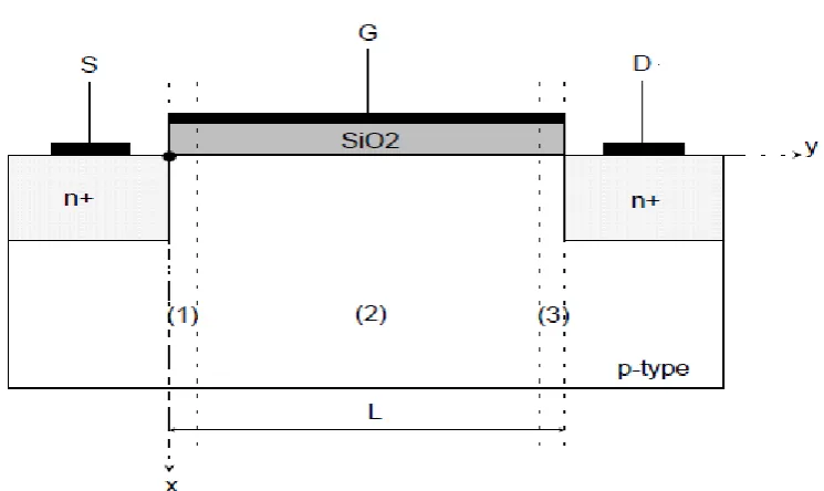
Analytical or semi-analytical modeling of MOSFET characteristics is usually based on the so-called Gradual Channel Approximation (GCA). In this approximation, we assume that the gradient of the electric field in the y direction, ∂F/∂y is much smaller than the gradient of the electric field in the x direction ,∂F/∂x. Which enable us to determine the inversion and depletion
charge densities under the gate in terms of a one-dimensional electrostatic problem for the direction perpendicular to the channel. By applying of the two dimensional Poisson's equation for the semiconductor, refer to Fig. 2.1 region (2),
(2.2.1)
if we assume that the GCA is valid equation 2.2.1 may be approximated to the following one dimensional differential equation
(2.2.2)
we approach the source and drain junctions, the GCA becomes invalid (Fig. 2.1 regions (1) and (3)) because of the increasing longitudinal field due to the pn junctions which make ∂F/∂y comparable or even larger than ∂F/∂x . However, for the long channel MOSFET's these transition regions can be
neglected with respect to the total length of the device. In order to account for the effect of these regions, it is necessary to use two dimensional analysis requiring a numerical solution of 2.2.1.
Validity of the GCA
The validity of GCA can be checked by making rough estimates of the variation in the longitudinal and vertical field components. We will establish expressions that allow the GCA to be checked under strong inversion.
(2.2.3)
For a MOSFET at 300K with L = 1.0μm, tox = 30 nm, VGS-VT = 0.5, and VDS = 0.5 V, the left
hand side of inequality 2.2.3 is ∼ 2300, indicating that the the GCA is a very good approximation for
such a MOSFET. This also implies that the GCA can be valid even in submicron MOSFETs, provided that VGSVT is not too small.
2.3 The long channel current model
The derivation of the dc drain current relationship recognizes that, in general, the current in the channel of a MOSFET can be caused by both drift and diffusion current. In an NMOSFET we may assume the following resonable approximation :
iii- No sources or sinks in the channel.
Note that in weak inversion the surface potential along the channel in long channel MOSFETs is almost constant. Thus ∂Fy/∂y is very small, implying that ∂Fy/∂y<<∂Fx/∂x. Thus in long channel
MOSFET the GCA is valid both in strong and weak inversion regions . Which enable us to reach to the following general relationship of drain current.
General Drift-Diffusion current equation in MOSFET:
This is the drift-diffusion drain current of the form
(2.3.1)
where μn is the electron surface mobility in the channel, W is the channel width, Qi is the inversion charge density per unit area, φc is the quasi Fermi potential (the difference between Efn at the surface of the semiconductor a d Efp in the bulk of the semiconductor), ψs is the surface potential referenced to the bulk potential, and φt is the thermal voltage (=kT/q). The first term is the drift current
component, while the second term is the diffusion current component. In both components, μn is the electrons' surface mobility being less than the mobility in the bulk due to surface scattering.
Voltage-Charge equation from the Transverse electric field:
In order to eliminate the electron charge density Qi term in the current charge equation, a second relationship is required that relates the electron charge density to the applied potentials. Using the relationship between voltage and charge appearing across the MOS capacitor we have
Cox (VG -φ ms -ψ s )= -(Qi+QB+Qox+Qit ) (2.3.2)
where VG is the gate voltage referenced to the bulk potential, φms is the metal semiconductor work function difference, QB is the depletion (bulk impurity) charge density per unit area, Qox is the sum of the effective net oxide charge per unit area at the Si-SiO2 interface, and Qit is the interface trapped charge density per unit area. Different approximations have been introduced in order to express the different MOS charges (QB, Qox, Qit) in terms of the applied voltages, then
using eq. (2.3.2) to compute the inversion charge density Qi. The resulting charge is then used in eq. (2.3.1) to determine the drain current; Four main approaches then follow, after them we shall discuss the proposed approach recently developed in ICL1 and modified by this work.
Interconnect simulation models:
The classical long-channel Pao and Sah model
drain current equation is therfore general, but as a result requires numerical integration in two dimensions, which limits its application in CAD tools.
Approximations:
i . Gradual Channel Approximation is used. ii . Constant mobility is assumed.
iii . Uniform substrate doping is considered. Advantages:
i . It is physically based.
ii . It gives a continuous representation of the device characteristics from weak to strong inversion even to the saturation mode of operation.
Disadvantages:
i. It requires excessive computational requriments since it requires numerical integration in two dimension, rendering it unsuitable to be used for circuit CAD.
The charge-sheet based models
The limited practical utility of the Pao-Sah model motivated a search for an approximate advanced analytical model, that is still accurate over a wide range of operating conditions. The charge sheet model, introduced separately by Bacarani and Brews in 1978, has become the most widely adopted long channel MOSFET model that is accurate over the entire range of inversion. In this model the inversion layer is supposed to be a charge sheet of infinitesimal thickness [11,15,16] (charge sheet approximation). The inversion charge density Qi can then be calculated in terms of the surface potential ψs. The drain current (2.3.1) is then expressed in terms of the surface potential at the
source and drain boundaries of the channel. Approximations:
i . Gradual Channel Approximation is used.
ii . The mobility is assumed to be proportional to the electric field and is constant with position along the channel.
iii . Uniform substrate doping is considered. Advantages:
i . It is physically based.
ii . It gives a continuous representation of the device characteristics from weak to strong inversion even to the saturation mode of operation.
ii . The charge sheet approximation introduces negligibly small error, and it is more computationally efficient than the classical model.
i . The boundary surface potentials cannot be expressed explicitly in terms of the bias voltages applied to the device, but must be found by a numerical process.
ii . The model is not valid in depletion or accumulation.
Different approaches have been introduced to circumvent this disadvantage. In it is shown that accurate numerical solutions for these surface potentials can be obtained with negligible computation time penalty. In the surface potentials are computed using cubic splines functions. In the implicit equation including the surface potential is replaced by an approximate function. Although all of these approaches have given good results, they have neglected the effect of the interface trap charge which is important in determining the subthreshold characteristics of the device, namely the subthreshold swing (the gate voltage swing needed to reduce the current by one decade).
Bulk Charge Model
The Bulk Charge model also known as variable depletion charge model, was developed in 1964, describes the MOSFET drain current only in strong inversion but of course has less computational requirements.
Approximations :
i . Drift current component only is considered ii . Constant surface potential is assumed iii . Id considered zero below threshold Advantages :
i . Less computational time than the charge sheet model Disadvantages :
i . The subthreshold region not defined
Square law model
This model has great popularity, when a first estimate to device operation, or simulating a circuit with a large number of devices is required. This model is obtained from the bulk charge model, on the assumption that VDS << 2φf+VBS .
i . Drift current component only is considered ii . Constant surface potential is assumed iii . Id considered zero below threshold iv . VDS << 2φf+VBS
Advantages :
i . Very small computational time than any other model ii . Suitable for hand calculations
Disadvantages :
ii . Overestimates the drain current in saturation region Approximate models
There exists a large number of introduced approximate models. All of these models originate from Brews' charge sheet model, where approximations to the surface potentials in various operating regions of the device have been used. This leads to different current equations each valid only in a specific region. The resulting equations are then empirically joined using different mathematical conditions of continuity.
Advantages:
i . They have good accuracy in the desired region of operation.
ii . They are very efficient from the point of view of computational time. Disadvantages:
i . The error increases in the transition regions between different modes of operations. ii . They include many non-physical fitting parameters.
Modified charge sheet model
The last discussed MOSFET models, have a common illness, no interface charges are included which play a great role in subthreshold region. So a modified model to the charge sheet model, which include the effect of interface charges is carried out in ICL, and will be presented now. The derivation begins by rewriting equation (2.3.1) in the following form :
I D = I D1+ I D2 (2.3.6.1)
where ID1 is due to the presence of drift:
2.3.6.2) and ID2 is due to the presence of diffusion:
(2.3.6.3)
after mathematical manipulation and following the same approximations as charge sheet model we reach the following drain current equations:
(2.3.6.5)
where ψs0 is the surface potential at the source end of the channel, ψsL is the surface potential at the
drain end of the channel, both are referred to the bulk. And their values are computed from the following two implicit equations.
(2.3.6.6)
UNIT III COMBINATIONAL AND SEQUENTIAL CIRCUIT DESIGN
Circuit families and its comparison:
The method of logical effort does not apply to arbitrary transistor networks, but only to logic gates. A logic gate has one or more inputs and one output, subject to the following restrictions: _ The gate of each transistor is connected to an input, a power supply, or the output; and _ Inputs are connected only to transistor gates. The first condition rules out multiple logic gates masquerading as one, and the second keeps inputs from being connected to transistor sources or drains, as in transmission gates without explicit drivers.
Pseudo-NMOS circuits
PSEUDO-NMOS CIRCUITS
is just the pullup current, 1/3. The inverter and NOR gate have an input capacitance of 4/3. The falling logical effort is the input capacitance divided by that of an inverter with the same output current, or The rising logical effort is three times greater, because the current produced on a rising transition is only one third that of a falling transition. The average logical effort is g = (4=9+4=3)=2 = 8. This is independent of the number of inputs, explaining why pseudo-NMOS is a
way to build fast wide NOR gates. Table 10.1 shows the rising, falling, and average logical efforts of other pseudo-NMOS gates, assuming _ = 2 and a 4:1 pulldown to pullup strength ratio. Comparing this with Table 4.1 shows that pseudo-NMOS multiplexers are slightly better than CMOS multiplexers and that NMOS NAND gates are worse than CMOS NAND gates. Since pseudo-NMOS logic consumes power even when not switching, it is best used for critical NOR functions where it shows greatest advantage. Similar analysis can be used to compute the logical effort of other logic technologies, such as classic NMOS and bipolar and GaAs. The logical efforts should be normalized so that an inverter in the particular technology has an average logical effort of 1.
10.1.1 Symmetric NOR gates
equal to that of a unit inverter, as we had found in the analysis of pseudo-NMOS NOR gates. The pullup current comes from two PMOS transistors in parallel and is thus 2=3 that of a unit inverter. Therefore, the logical effort is 2=3 for a falling output and 1 for a rising output. The average effort is g = 5=6, which is better than that of a pseudo-NMOS NOR and far superior to that of a static CMOS NOR! and even for NAND gates. Exercises 10-3 and 10-4 examine the design and logical effort of such structures.
Domino circuits
Pseudo-NMOS gates eliminate the bulky PMOS transistors loading the inputs, but pay the price of quiescent power dissipation and contention between the pullup and pulldown transistors. Dynamic gates offer even better logical effort and lower power consumption by using a clocked precharge transistor instead of a pullup that is always conducting. The dynamic gate is precharged HIGH then may evaluate LOW through an NMOS stack. Unfortunately, if one dynamic inverter directly drives another, a race can corrupt the result. When the clock rises, both outputs have been precharged HIGH.
The HIGH input to the first gate causes its output to fall, but the second gate’s output also falls in response to its initial HIGH input. The circuit therefore produces an incorrect result because the second output will never rise during evaluation, as shown in Figure 10.3. Domino circuits solve this problem by using inverting static gates between dynamic gates so that the input to each dynamic gate is initially LOW. The falling dynamic output and rising static output ripple through a chain of gates like a chain of toppling dominos. In summary, domino logic runs 1:5 to 2 times faster than static CMOS logic [2] because dynamic gates present a much lower input capacitance for the same output current and have a lower switching threshold, and because the inverting static gate can be skewed to favor the critical monotonically rising evaluation edges. Figure shows some domino gates. Each domino gate consists of a dynamic gate followed by an inverting static gate1. The static gate is often but not always an inverter. Since the dynamic gate’s output falls monotonically during evaluation, the
the next section. The logical effort of a domino gate is then the product of the logical effort of the dynamic gate and of the high-skew gate. Remember that a domino gate counts as two stages when choosing the best number of stages. A dynamic gate may be designed with or without a clocked evaluation transistor; the extra transistor slows the gate but eliminates any path between power and ground during precharge when the inputs are still high. Some dynamic gates include weak PMOS transistors called keepers so that the dynamic output will remain driven if the clock stops high. Domino designers face a number of questions when selecting a circuit topology. How many stages should be used? Should the static gates be inverters, or should they perform logic? How should precharge transistors and keepers be sized? What is the benefit of removing the clocked evaluation transistors? We will show that domino logic should be designed with a stage effort of 2–2:75, rather than 4 that we found for static logic. Therefore, paths tend to use more stages and it is rarely beneficial to perform logic with the inverting static gates.
Logic power logic design:
Is to Reduce dynamic power and static power in a circuit – a:
– C: – VDD: – f:
Reduce static power,Reduce dynamic power – a: clock gating, sleep mode
– C: small transistors (esp. on clock), short wires – VDD:
– f:
Reduce static power, Reduce dynamic power – a: clock gating, sleep mode
– C: small transistors (esp. on clock), short wires – VDD: lowest suitable voltage
– f: lowest suitable frequency
Reduce static power
– Selectively use ratioed circuits – Selectively use low Vt devices
– Leakage reduction: stacked devices, body bias, low temperature.
Circuit design of latches and flip flops:
which the outputs at any instant are dependent not only upon the inputs present at that instant but also upon the past history (sequence) of inputs.
Sequential circuits are classified into:
The block diagram of a sequential circuit is shown below:
Synchronous sequential circuits – Their behaviour is determined by the values of the signals
at only discrete instants of time.
Asynchronous sequential circuits – Their behaviour is immediately affected by the input
signal changes.
The basic logic element that provides memory in many sequential circuits is the flip-flop.
1. Latches
Latches form one class of flip-flops. This class is characterized by the fact that the timing of the output changes is not controlled. Although latches are useful for storing binary information and for the design of asynchronous sequential circuits, they are not practical for use in synchronous sequential circuits.
1.2 The SR Latch
It is a circuit with two cross-coupled NOR gates or two cross-coupled NAND gates. The one with NOR gates is shown below:
changed. An SR latch with control input is shown below: The control input C acts as an enable signal form the other two inputs. An indeterminate condition occurs when all three inputs are equal to 1. This condition makes the circuit difficult to manage and is seldom used in practice. Nevertheless, it is an important circuit because other latches and flip-flops are realized from it.
The Gated D Latch
One way to eliminate the undesirable condition of the indeterminate state in the SR latch is to ensure that inputs S and R are never equal to 1 at the same time. This is done by the D latch:
Flip-Flops
Edge-Triggered D Flip-Flop
A D flip-flop may be realized with two D latches connected in a master-slave configuration: The circuit samples the D input and changes its Q output only at the negative-edge of the controlling clock signal (CLK). It is also possible to design the circuit so that the flip-flop output changes on the positive edge of the clock (transition from 0 to 1). This happens in a flipflop that has an additional inverter between the CLK terminal and the junction between the other inverter and input C on the master latch. An efficient realization of a positive edge-triggered D flip-flop uses three SR latches:
The graphic symbol for the edge-triggered D flipflop is:
Other Flip-Flops
Characteristic Tables
A characteristic table defines the logical properties of a flip-flop by describing its operation in tabular form. The flip-flops characteristic tables are:
Q(t) refers to the present state prior to the application of a clock edge.
Q(t + 1) is the next state one clock period later. The clock edge input is not included in the characteristic tables, but is implied to occur between time t and t + 1.
Characteristic Equations
The logical properties of a flip-flop as described in its characteristic table can be expressed also algebraically with a characteristic equation. For the D flip-flop the characteristic equation is: Q(t +1) = D
It states that the next state of the output will be equal to the value of input D in the present state.
The characteristic equation for the JK flip-flop is:
where Q is the value of the flip-flop output prior to the