Research article Available online www.ijsrr.org
ISSN: 2279–0543
International Journal of Scientific Research and Reviews
Single Input DC to Multiple Output DC Buck Converter
K. Ravi Kumar
1and M. Sai Kumar
2*1
Associate Professor, Electrical and Electronics Engineering, Vasavi College of Engineering, Hyderabad, Telangana, India.
2
PG Scholar, Electrical and Electronics EngineeringVasavi College of Engineering, Hyderabad, Telangana,India,
[email protected], [email protected]
ABSTRACT
This paper proposes a new single-input three-outputDC-DC buck converter. The proposed topology hassingle input DC to multiple output dc-dc converter which has two less switching devices than that of a conventional converter. This decrease in switching devices leads to lesser cost and a more even division of power losses among the switching devices. A comprehensive small signal Modeling and control strategies for the dc-dc converter will be presented. Simulation and experimental results are presented to validate the theoretical expectations. The simulation is performed using PSIM.
KEYWORDS:
AC-DC converter, DC-DC buck converter, bidirectional, unidirectional, small signal analysis.*
Corresponding Author:
M. Sai Kumar
INTRODUCTION
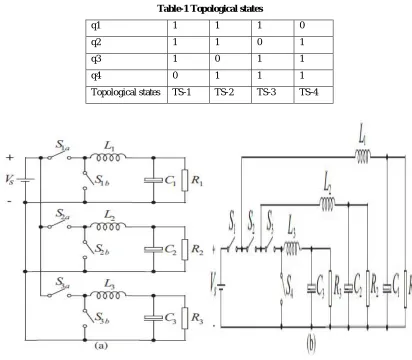
Applications of DC-DC converters include renewable energy systems1, hybrid electric vehicles5, 6, and uninterrupted power supplies7,8. DC-DC converters can be made with both unidirectional and bidirectional power flow capabilities1-4. The unidirectional converter is made using a power switch, a power diode, and an LC filter1-3, 14. The bidirectional converter is achieved by removing the power diode and placing a power switch in parallel with the LC filter. Fig. 1(a) shows that by replicating the bidirectional circuit three times, a bidirectional single-input three-output converter can be achieved. In13, bidirectional DC-DC converters were shown to require smaller sized filters than that of a unidirectional converter. Faster dynamic response and lower device stress were also noted in the bidirectional converter13. In12, a bidirectional DC-DC converter topology was proposed for use in applications that do not require magnetic components.
Applications such as communication systems and battery management systems require a DC-DC buck converter with multiple controlled outputs. In17, a configuration was proposed that uses a single inductor for obtaining three controlled outputs. A three switch DC-DC buck converter topology was proposed in18 that can be used in applications that require two controlled outputs. In this paper, a novel single-input three-output DC-DC buck converter has proposed. The proposed topology requires two fewer power switches than that of the conventional single-input three-output DC-DC buck converter. The differences of these converters are highlighted in Fig. 1.
PROPOSED CONVERTER
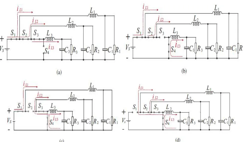
The proposed topology consists of four power switches (S1, S2, S3, and S4) and three low pass filters (L1-C1, L2- C2, and L3-C3). The state of the each switch is represented by binary variables, that is, qx= 0 indicates that switch Sxis OFF, and qx= 1 indicate switch Sxis ON, where x=1, 2, 3, and 4. Since there are four switches and two states for each switch, we attain 16 ways of operating the converter. Of these 16 states, only four are operational. All the other switching combinations should be avoided because in that particular instant output of any one of the load is discontinuous. Table 1 provides the topological states (TS) where TS-1, TS-2, TS-3, and TS-4 represent the operational states. It can be observed from Fig.2 that:
For TS-2 (q1 = 1, q2 = 0, q3 = 1, and q4 = 1), the input energy is provided to R1, L1, R2, and L2. Energy stored in inductor L3 is dissipated. In Fig. 2(b), iL3 flows in the closed path formed by switch S4.
For TS-3 (q1 = 1, q2 = 1, q3 = 0, and q4 = 1), the input energy is provided to R1 and L1. Energy stored in inductors L2 and L3 is dissipated. This means the current iL2 will be flowing in the closed path (see Fig. 2(c)) formed by switch S3 and S4, and current iL3 will be flowing in the closed path formed by switch S4.
Finally, in TS-4 (q1 = 1, q2 = 1, q3 = 1, and q4 = 0), energy provided to all the inductors dissipates to their respective loads. Currents iL1, iL2, and iL3 are discharged during this state (see Fig. 2(d)).
Table-1 Topological states
q1 1 1 1 0
q2 1 1 0 1
q3 1 0 1 1
q4 0 1 1 1
Topological states TS-1 TS-2 TS-3 TS-4
Fig. 1.Synchronous single-input multiple-output DC-DC converter for (a) conventional topology, and (b)
STEADY STATE ANALYSIS
The proposed converter is assumed to be operating in continuous conduction mode with inductor waveforms shown in Fig. 3(a). From the waveforms and topological states obtained in the preceding sections, it can be deduced that variable VR1 controls output voltage
Vo1, variable VR2 controls output voltage Vo2, and variable VR3 controls output voltage Vo3.
Since the average inductor voltage is zero, the following equations can be obtained:
( − ) = ( − ) (1)
( − )( − ) = (2)
( − )( − ) = (3)
Here Ton1, Ton2, and Ton3 are the time periods for the duration of which respective
PWM generators 1, 2, and 3 are producing logic “1” at their output.
From the above equations, the output voltages can be derived as a function of their duty cycles and supply voltage. The output voltages are represented by the following equations
= . (4)
= 1− . (5)
= 1− . (6)
whereDgen1, Dgen2, and Dgen3 represent the duty cycles.
INDEPENDENT OUTPUT VOLTAGE GENERATION
The duty cycle of switch S1 can be ranging from a minimum value of 0 to a maximum
value of 1. Assuming the duty cycle for switch S1 is D1 = 3/4, the output voltage on load 1
would be 75% of the input voltage. The duty cycle of switch S2 can be ranging from 0 to D1.
Similarly, the duty cycle of the switch S3 can be ranging from 0 to D2. As a consequence, the
Fig. 2. Modes of operation: (a) TS-1, (b) TS-2, (c) TS-3, and (d) TS-4.
PULSE WIDTH MODULATION
The four switches discussed in the preceding section are operated using pulse width modulation(PWM) technique. This modulation approach deals with a comparison of reference voltages ∗ , ∗ , and ∗ with a saw-tooth waveform. The output of this comparison goes through a logic circuit which dictates the state of the switches. These reference voltages will control the output voltages across R1, R2, and R3. Note that the output
of the first PWM generator will be the difference between the saw-tooth waveform and ∗ . Likewise, the output of the second and third PWM generator will be obtained with respect to
∗ , and ∗ respectively.
The PWM logic circuit realization is shown in Fig. 3(d) is used for controlling the duty cycle of the switches. This circuit is built, based on few conclusions that were developed from the operation of the converter described during its corresponding topological state.
The charging of inductor L1 is entirely dependent on switch S1. Hence, the first PWM
generator can be directly connected to switch S1 to control the output voltages V01 or the state
of inductor L1.
During the topological state (TS-4), switch S2 is “ON,” at the same time, inductor L2
inductor L2 is not dependent on the state of the switch S2. Note that, switch S2 should be
operated in such a way thattopological states TS-1 and TS-2 remain for an interval that can be defined by the second PWM generator. In addition, switch S2 should be controlled in such a
way that prohibited states are avoided. These requirements are achieved by using a two input “OR” gate and a “NOT” gate shown in Fig. 3(c).
By similar observation, switch S3 should be operated in such a way that topological
state TS-1 remains for an interval of time that is defined by third PWM generator. Switch S3
should also be controlled in such a way that, it stays“ON” when either of switches S1 or S2
turns “OFF.” These requirements can be satisfied by using a three input “OR” gatein which, the output of third PWM generator and the inverse of the first and second generators are connected.
Finally, switch S4 defined by the state of the switches S1, S2, and S3. This means that
the function of switch S4 in the circuitry is to avoid the prohibited states. This control of the switch can be achieved by using a “NAND” gate. Fig. 3(c) shows the gating signals that are obtained for switches S1, S2, S3, and S4 respectively.
SMALL SIGNAL ANALYSIS
In the case of designing a controller or assessing the performance for a converter, the linearization techniques discussed in 19 can be used. In order to have a clear understanding on the dynamics of the novel configuration, small signal analysis is performed and transfer functions are derived. Following the procedure outlined in 20.Kirchoff’s laws is applied on the topological states, and their corresponding equations are as follows:
Topological state-1:
+ = (7)
+ = (8)
+ = (9)
+ = (10)
+ = (11)
Topological state-2:
+ = (13)
+ = (14)
+ = 0 15)
+ = (16)
+ = (17)
− = (18)
Topological state-3:
+ = (19)
+ = 0 (20)
+ = 0 21)
+ = (22)
− = 23)
− = (24)
Topological state-4:
+ = 0 25)
+ = 0 (26)
+ = 0 (27)
− = (28)
− = (29)
Fig. 3. (a)Voltage and current waveforms for L1, L2, and L3, (b) Gating signal for switches S1, S2, S3, and
S4 respectively, (c) Logic circuits for definingthe state of switches S2, and S3, (d) PWM implementation
for the proposed topology.
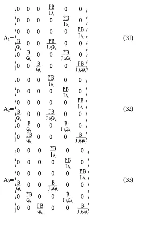
The above equations are expressed in the form of state space equations and their resultant state space matrices are represented below. Here, A1, B1, and C1 are the state space
matrices which are obtained for the topological state-1. Similarly, the corresponding state space equations for TS-2, TS-3, and TS-4 were also derived and are as follows:
A1=
⎣ ⎢ ⎢ ⎢ ⎢ ⎢ ⎢ ⎢ ⎢
⎡0 0 0 0 0
0 0 0 0 0
0 0 0 0 0
0 0 0 0
0 0 0 0
0 0 0 0 ⎦⎥
⎥ ⎥ ⎥ ⎥ ⎥ ⎥ ⎥ ⎤ (31)
A2=
⎣ ⎢ ⎢ ⎢ ⎢ ⎢ ⎢ ⎢ ⎢
⎡0 0 0 0 0
0 0 0 0 0
0 0 0 0 0
0 0 0 0
0 0 0 0
0 0 0 0 ⎦⎥
⎥ ⎥ ⎥ ⎥ ⎥ ⎥ ⎥ ⎤ (32)
A3=
⎣ ⎢ ⎢ ⎢ ⎢ ⎢ ⎢ ⎢ ⎢
⎡0 0 0 0 0
0 0 0 0 0
0 0 0 0 0
0 0 0 0
0 0 0 0
0 0 0 0 ⎦⎥
A4= ⎣ ⎢ ⎢ ⎢ ⎢ ⎢ ⎢ ⎢ ⎢
⎡0 0 0 0 0
0 0 0 0 0
0 0 0 0 0
0 0 0 0
0 0 0 0
0 0 0 0 ⎦⎥
⎥ ⎥ ⎥ ⎥ ⎥ ⎥ ⎥ ⎤ (34)
B1 =
⎣ ⎢ ⎢ ⎢ ⎢ ⎢ ⎢ ⎡ 0 0 0⎦ ⎥ ⎥ ⎥ ⎥ ⎥ ⎥ ⎤
B2 =
⎣ ⎢ ⎢ ⎢ ⎢ ⎢ ⎡ 0 0 0 0⎦ ⎥ ⎥ ⎥ ⎥ ⎥ ⎤
B3 =
⎣ ⎢ ⎢ ⎢ ⎢ ⎢ ⎡ 0 0 0 0 0⎦ ⎥ ⎥ ⎥ ⎥ ⎥ ⎤
B4 =
⎣ ⎢ ⎢ ⎢ ⎢ ⎡00
0 0 0 0⎦ ⎥ ⎥ ⎥ ⎥ ⎤ (35)
C1 = C2 = C3 = C4 = [0 0 0 1 1 1] (36)
From the topological states that were depicted in the Fig. 2, it is good to mention that the converter operates in these states for a definite period of time. If Da, Db,Dc,and Ddare
considered as duty cycles for the respective topologies TS- 1, TS-2, TS-3, and TS-4. State space matrices for the whole converter are derived by adding the resultant matrices, which are obtained by multiplying the above state space matrices (31)-(34) with their corresponding topological duty cycles. Equations represented below are the state space equations for the proposed single input triple output DC-DC buck converter.
= ( )+ ( ) (37)
= ( )+ ( ) (38)
= ( )+ ( ) (39)
= ( )( )+( ) (40)
= ( )( )+( ) (41)
Laplace transformation is applied on the converter’s state space equations, and transfer functions are derived. The obtained transfer functions are:
( ) ( ) =
( )( )
( ) ( ) ( ) (43) ( )
( ) =
( )
( ) ( ) (44) ( )
( ) =
( )
( ) ( ) ( ) (45)
Where = ( + + − ), = ( + − − ),and
= ( − − − )
In order to express the output variables with respect to input and control parameters, topological duty cycles Da, Db, Dc, and Ddare correlated with the duty cycles generated by
PWM generators 1, 2, and 3. Resultant expressions are programmed in the following equations.
+ + = (46)
+ = (47)
= (48)
Since the state space frequency of DC-DC converter is zero, by Substituting the above equations(46)-(48) in (43)-(45), the transfer functions can be minimized into the following expressions.
( )
( ) = (49)
( )
( ) = (50)
( )
( ) = (51)
COMPARISON
OF
SWITCHING
LOSSES
AMONG
THE
TOPOLOGIES
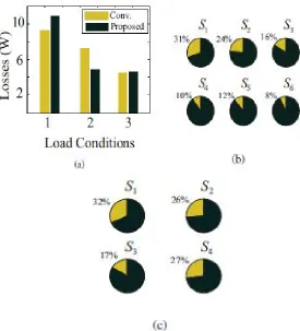
modules that are used to calculate the losses. Specifically, the one used for this comparison was for the IRFP 460 MOSFET. Fig. 4(a) shows the total semiconductor losses for both topologies. It can be seen that under some load conditions, the proposed topology offers semiconductor losses that are better, poorer or even the same as for a conventional one. Even though it does not always offer better efficiency, the proposed circuit does offer better power loss distribution among the switches in every case, which can be seen by comparing Fig. 4(b) and 4(c). The proposed and conventional circuit were put under the exact same conditions during the tests, that is Vs =300V ,L1 = L2 = L3 = 0.001H, and C1 = C2 = C3 = 0.00012F.
Under load conditions of R1 = R2 = R3= 100Ω, the conventional topology had 97% efficiency
while the proposed converter had 96% efficiency. Under load conditions R1= 3000Ω, R2 =
2000Ω, and R3= 50Ω, the conventional topology had an efficiency of 91%, and the proposed
topology had an efficiency of 93%. Both topologies operated at 94% efficiency under load conditions R1= 3000Ω and R2 = R3= 2000Ω.
THERMAL ANALYSIS
The junction temperature of the switches in both the proposed and traditional topology was simulated using an equivalent thermal circuit model. Fig. 5 shows this equivalent circuit for one of the switches. The three thermal resistances that are represented (from left to right) are; Thermal resistance junction to case (RJC), the thermal resistance of the thermal interface material (RTIM), and thermal resistance of the heat sink (RH). For simplification purposes, an only steady-state analysis was performed.
Both topologies were simulated under the conditions Vs=300V, L1 = L2 = L3 = 0.001H,
C1 = C2 = C3 = 0.00012F, R1= 3000Ω, R2= 2000Ω, R3= 50Ω, ambient temperature= 70ºF,
Fig. 4. (a) Semiconductor losses under different load conditions, (b)Traditional semiconductor loss
distribution. (c) Proposed semiconductor loss distribution.
Fig. 5. Equivalent thermal model
Table2 Resultant Power Losses and Temperatures for the Proposed Topology
Switch Losses Temperatures (degree Fahrenheit)
S1
S2
S3
S4
1.6 1.2 0.6 1.5
Obtained losses and the temperatures at each of the switchcasings for the proposed topology are presented in Table 2.Table 3 lists the losses and temperatures for each switchpresent in the conventional topology.
Table3 Power Losses and Temperatures Recorded for the Conventional Topology
Switch Losses Temperatures (degree Fahrenheit)
S1
S2
S3
S4
S5
S6
0.99 0.95 0.73 0.75 2.02 1.99
70.7 70.6 70.5 70.5 71.4 71.4
These simulation results can be validated mathematically, by using the following equation.
Temperature =(Ambienttemperature)+ (RJC + RTIM + RH) * (Losses) (52) When comparing the switching losses presented in Table III, it can be noted that similar temperatures were obtained, and only negligible differences were observed among the losses obtained across the switches.
SIMULATION RESULTS
Considering Vs= 100V ,L1 = L2 = L3 = 0.06mH, C1 = C2 = C3 = 0.0022F, R1 = R2 = R3
= 100Ω VR1=55V, VR2=30V, and VR3=15V as the parameters, the simulation of the proposed
topology is analyzed using PSIM.
Simulation results obtained for the gating signals, output voltages, and regulating the output voltages for are shown in Fig. 6 and Fig. 7. Simulation results achieved are shown in the Fig. 8, Fig. 9, and Fig. 10. Fig. 8 shows the currents and voltages across inductor L1 and
the output voltage V01. Fig. 9, shows the current IL2 and voltages across inductor L2 and at the
load R2. Fig. 10 shows their corresponding simulation results. Fig. 12(a), shows the current
Fig. 6. Gating signal
Fig. 7. Input and Output Voltages
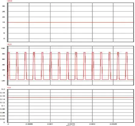
Fig. 9.output voltage V02, Inductor voltage VL2, andInductor current IL2
Fig. 10. Output voltage V03, Inductor voltage VL3, andInductor current IL1
CONCLUSION
REFERENCES
1. Ghodke, D., Chatterjee, K., Fernandes, B. Modified soft-switched phase three-level dc-dc converter for high-power applications having extended duty cycle range, IEEE Trans. Ind. Electron., 2012;59(9): 3362–3372
2. Pahlevaninezhad, M., Drobnik, J., Jain, P., Bakhshai, A. A load adaptive control approach for a zero-voltage-switching dc-dc converter used for electric vehicles, IEEE Trans. Ind. Electron., 2012; 59(2):920-933.
3. Yang, L.-S., Liang, T.-J. Analysis and implementation of a novel bidirectional dc-dc converter, IEEE Trans. Ind. Electron., 2012; 59(1):422-434.
4. Lee, J.-Y., Jeong, Y.-S., Han, B.-M. An isolated dc-dc converter using high-frequency unregulated LLC resonant converter for fuel cell applications”, IEEE Trans. Ind. Electron., 201; 58 (7):2926-2934.
5. Ouyang, Z., Zhang, Z., Thomsen, O.C., Andersen, M.A.E. Planar-integrated magnetics (PIM) module in hybrid bidirectional dc-dc converter for fuel cell application, IEEE Trans. Power Electron., 2011; 26(11): 3254-3264.
6. Wang, L., Wang, Z., Li, H. Asymmetrical duty cycle control and decoupled power ow design of a three-port bidirectional dc-dc converter for fuel cell vehicle application, IEEE Trans. Power Electron. 2012; 27:891-904.
7. Nasiri, A., Nie, Z., Bekiarov, S.B., Emadi, A. An on-line ups system with power factor correction and electric isolation using BIFRED converter, IEEE Trans. Power Electron., 2008; 55(2):722–730.
8. Zhang, Z., Ouyang, Z., Thomsen, O.C., Andersen, M.A.E. Analysis and design of a bi-directional isolated dc-dc converter for fuel cells and super capacitors hybrid system, IEEE Trans. Power Electron. 2012;27(2): 848-859.
9. Wu, H., Lu, J., Shi, W., Xing, Y. Non-isolated bidirectional dc-dc converters with negative-coupled inductor, IEEE Trans. Power Electron., 2012;27(5):2231-2235. 10.Tan, N.M.L., Abe, T., Akagi, H. Design and performance of a bidirectional isolated
dc-dc converter for a battery energy storage system, IEEE Trans. Power Electron., 2012; 27(2): 1237- 1248.
12.Shen, M., Peng, F.Z., Tolbert, L.M.: Multilevel dc-dc power conversion system with multiple dc sources, IEEE Trans. Power Electron., 2008; 23(1): 420-426
13.Ni, L., Patterson, D.J., Hudgins, J.L. High power current sensorless bidirectional 16-phase interleaved dc-dc converter for hybrid vehicle application, IEEE Trans. Power Electron., 2012; 27 (3):1141-1151.
14.Li, W., He, X. A family of isolated interleaved boost and buck converters with winding-cross-coupled inductors, IEEE Trans. Power Electron., 2008; 23(5): 3164-3173
15.Belloni, E.B.M., Maloberti, F. On the design of singleinductor double-output dc-dc buck, boost and buck- boost converters. 15th IEEE Int. Conf. on Electronics, Circuits and Systems, ICECS 2008, September, 2008;626-629
16.Rojas-Gonzalez, M., Torres, J., Sanchez- Sinencio, E., Kumar, P. An integrated dual-output buck converter based on sliding mode control. IEEE Third Latin American Symp. Circuits and System, 2012; 14.
17.Cavalcanti, M.C., da Silva, E., Boroyevich, D., Dong, W.,Jacobina, C.B. A feasible loss model for IGBT in soft-switching inverters. Proc. IEEE PESC, 2003;1845-1850 18.E. C. dos Santos Jr. Dual-output DC-DC Buck converters with bidirectional and
unidirectional Characteristics, IET Transactions on Power Electronics, May2013; 6(5): 999–1009.
19.M. K. Reddy, C.Kalyani, M.Uthra and D.Elangovan: A small signal analysis of dc-dc boost converter, Indian Journal of Science and Technology, 2015.
20.S. Yang, K.Goto, Y. Imamura and M. Shoyama, Dynamic characteristics of bidirectional dc-dc converter using state-space averaging method,INTELEC, 2012.
Dr.K.RAVI KUMAR
He received B.Tech (EEE) and M.Tech (P.E) from the Jawaharlal Nehru Technological University Hyderabad in 1998 and 2005 respectively. Heobtained his PhD degree in Electrical Engineering from NITWarangal under the guidance of Prof. M. Sydulu in 2016. Since 2001, He has been working as Associate Professor with the Electrical & Electronics Engineering department, Vasavi College of Engineering, Hyderabad. His interests include power system optimization, AI applications to power systems, Economic operation of power systems, power quality, power system stability, contingency analysis, smart grid, renewable energy systems and power electronic.