Electronic Transport Processes In
Two-Dimensional Solid Solutions
Salim Asadov, Institute of Catalysis and
Inorganic Chemistry, Azerbaijan National Academy of
Sciences,
av. H. Javid 113, AZ-1143 Baku, Azerbaijan
Solmaz Mustafaeva, Institute of Physics, Azerbaijan National Academy of
Sciences, av. H. Javid 131, AZ-1143 Baku, Azerbaijan
Kudrat Kelbaliev, Institute of Catalysis and
Inorganic Chemistry, Azerbaijan National Academy of
Sciences, av. H. Javid 113, AZ-1143 Baku, Azerbaijan
Abstract—We have synthesized and grew 2D single crystals GaSe1-xSx with a hexagonal structure. It
was established that the variable-range-hopping mechanism of dc-conductivity takes place in the GaSe1-xSx single crystals at low temperatures. The
parameters of localized states in the forbidden gap of studied crystals have been evaluated. Dielectric properties (loss tangent, real () and imaginary () parts of complex dielectric permittivity) and ac-conductivity across the layers) of the GaSe1-xSx
layered single crystals have been studied in the frequency range f = 5 104 to 3.5 107 Hz. The
results demonstrate that the dielectric dispersion in the GaSe1-xSx single crystals has a relaxation
nature. Over the studied frequency range, the ac-conductivity of the GaSe1-xSx crystals varies as f0.8,
characteristic of hopping conduction through localized states near the Fermi level. The Fermi-level density of states, the spread of their energies, and the mean hop distance and time have been estimated.
Keywords— single crystal GaSe1-xSx; charge transport; density of localized states; frequency dispersion; dielectric permittivity; loss tangent
I. INTRODUCTION
Only a few years ago, low dimensional structures were an esoteric concept, but now it is apparent they are likely to play a major role in the next generation of electronic devices. The study of 2D layered materials, especially monochalcogenides represented by GaX, is an active and rapidly growing field of research. This field may lead to fabrication of nanodevices in a layer-by-layer fashion using 2D materials. Gallium monochalcogenides (GaX, X – S, Se, Te) are layered compounds like graphite that can be readily reduced to two-dimensional (2D) form due to their strong in-plane bonding and weak interlayer van der Waals coupling. It is known that GaX form solid solutions, for example
x x 1
S
GaSe
. The band structure of 2D compounds, in particularGaSe
1xS
x, dramatically changes from bulk to single layer samples, going from indirect gap in bulkmaterials to direct gap in monolayers, underscoring the important role of interlayer coupling. In addition, their electronic properties are very sensitive to external conditions such as electric field, temperature, pressure or strain. The results of investigation of electrical, photoelectric, thermal and optical properties of these crystals were presented in the works [1–7].
x x 1
S
GaSe
-based materials, combining interesting electrical and optical properties, are potential candidates for use in various transducers, light modulators, and information storage units. However, until now not studied dc- and ac-electronic processes in layerGaSe
1xS
x crystals. The investigation of electric properties of materials in dc-and ac-electric fields gives information about the nature of charge transport and localization states in forbidden gap. For the establishment of mechanism of charge transport it is necessary to know the temperature and frequency dependences of dc-and ac-conductivity. The objectives of this work were to study the dc-and ac- electrical properties ofGaSe
1xS
xsingle crystals, to gain insight into the mechanism of charge transport in the crystals, and to evaluate the parameters of localized states in their band gap.II. MATERIALSANDMETHODS
Ga-5N gallium, B5 sulfur, and OSCh-17-3 selenium with impurity content no higher than 5 × 10⁻⁴ wt % were used in the synthesis of GaS and GaSe compounds. The synthesis was performed by melting starting elements taken in stoichiometric ratios in evacuated (pressure of 10–3 Pa) and sealed quartz ampules. The ampules were held for 6 – 8 h at a temperature higher than the liquidus temperature by 25 – 30 K (melting points of GaS and GaSe are 1288 and 1211 K, respectively) and then allowed to cool to room temperature. The prepared compounds GaS and GaSe were identified by DTA (a heating/cooling rate of 10 K/min) and powder X-ray diffraction analysis using the literature data for comparison. Solid solutions
x x 1
S
Vol. 3 Issue 8, August - 2017 stoichiometric weighed portions of preliminarily
prepared starting GaS and GaSe components in evacuated quartz ampoules.
Single crystals of
GaSe
1xS
xsolid solutions were grown by the Bridgman–Stockbarger method. Polycrystalline samples of the prepared compounds and solid solutions of specified compositions were ground and loaded into separate quartz ampules 8- to 10-cm-long with an inner diameter of 1 cm and sharpened ends. A quartz ampule with a sample was placed in the dual-zone furnace of a device for single crystal growth. In the course of crystal growth from a melt, the temperature of 1293 K (5 K higher than the melting point of GaS) was maintained in the upper zone of the furnace and the temperature of 1200 K (10 K lower than the melting point of GaSe) was maintained in the lower zone. The ampule was moved in the furnace at a rate of 0.3 – 0.5 cm/h, and the temperature gradient near the crystallization front was 25 ± 3 K. The abovementioned rate of movement of the ampule with a sample in the furnace was optimal for the growth of a nucleus of a single crystal. In other words during the preparation ofGaSe
-
GaS
single crystals by method of directional solidification the melt cooling rate was selected to ensure the crystallization front close to the flat. Due to concentration supercooling duringx x 1
S
GaSe
growth at speeds > 0.5 cm/h there is loss of morphological stability of a flat front and transition to the cell structure [7].The X-ray diffraction studies of the
GaSe
1xS
xsolid solutions were performed on a D2PHАSER-ray diffractometer using monochromatic CuKα radiation (Ni-filter). A single-crystal graphite plate used as a monochromator was placed in the path of a reflected beam. For example, for GaSe lattice parameters are: a = 3.755 ± 0.002 Å and с = 15.940 ± 0.005Å at room temperature. The GaSe crystals belong to the space groupP
6
m
2
and cleave readily along the (0001) plane.The bulk sample
GaSe
1xS
x, which is used in the experiments, was prepared by splitting the single crystal along the cleavage plane and hence the resultant surface was mirrow-like without any mechanical treatment. The samples for electrical measurements had the shape of rectangular plates. The thickness of the single-crystalGaSe
1xS
x samples was 300 – 500 m. Ag paste was used as a contact material to theGaSe
1xS
x samples. Dc-electric field from Ohmic region of current-voltage characteristic was applied crosswise to the natural layers of a GaS single crystal. All dc-electrical measurements were carried out in the temperature interval 116 – 294 К on samples placed into a cryostat with a temperature stabilization system (the stabilization accuracy is 0.02 K).The dielectric properties of the
GaSe
1xS
x single crystals were studied by a resonance technique [8] in the frequency range f = 5
104 to 3.5
107 Hz. Thesingle crystal
GaSe
1xS
x samples for dielectric measurements had the form of planar capacitors normal to the C axis of the crystals. Electrical contacts were made with silver paste. The dielectric properties of the samples were measured in the direction perpendicular to the layers of theGaSe
1xS
x single crystals. During the measurements, the samples were located in a shielded chamber. The thickness of thex x 1
S
GaSe
single-crystal samples ranged from 200 to 700 , and the area of the capacitor plates was equal to 7 10-2 cm2. All of the ac-measurements were performed at 300 K in electric fields corresponding to Ohmic current-voltage behavior. The accuracy in determining the sample capacitance and the merit factor Q = 1/tan δ of the measuring circuit was limited by reading errors. The capacitors were calibrated with an accuracy of ±0.1 pF. The reproducibility in the resonance position was ±0.2 pF in terms of capacitance and ±1.0 – 1.5 scale divisions in terms of Q. The largest deviations were 3–4 % in and 7 % in tan .III. RESULTS AND DISCUSSION
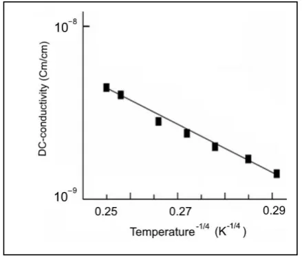
The experimental results of the investigations into the dc-electrical properties of the GaS single crystals in the temperature interval 116 – 294 К are presented below. The dependence of log on 1/T in GaS samples at temperatures T = 140 – 238 K is characterized by a monotonic decrease in the activation energy with a decrease in the temperature (fig. 1). This behavior of the dc-conductivity in GaSat low temperatures suggests that charge transfer occurs through the variable-range-hopping mechanism, provided the current is transferred by charge carriers at the states localized in the vicinity of the Fermi level [9].
Fig. 1. Temperature dependence of the dark dc-conductivity of a GaS single crystal
Fig. 2. Dependence of the conductivity of a GaS single crystal vs T-1/4
The slope of this curve (T0) allowed us to estimate the density of localized states near the Fermi level from the formula (N. Mott):
/
16
0 3F
T
ka
N
(1)where k is the Boltzmann constant, ɑ is the localization length.
The density of states NF was found to be equal to 6.2
1019 eV–1 cm–3. When calculating NF, the localization length for the GaS single crystal was taken as ɑ = 14 Å [10].We calculated also the average hopping distance in GaS according to the formula [9]:
4 / 1 0
/
)
(
)
8
/
3
(
)
(
T
a
T
T
R
(2)As a result, we found that, Rav = 46 Å. As is seen, the average jump distance Rav(T) in the GaS single crystal substantially exceeds the distance between the carrier localization centers.
From the condition [9]:
4
/
3
R
3N
F
E
/
2
1
(3)
we determined the scatter of trap states near the Fermi level (E). The scatter of the localized states is estimated as E = 0.08 eV.
The activation energy of the hopping conductivity is estimated as W = 0.07 eV from the formula [11]:
3/4
3
1/4/
N
a
kT
T
W
F
(4)We calculated also the concentration of trapping states (
N
t= 5 1018 cm-3) responsible for the hopping dc-conductivity in GaS single crystal, according to the formula
E
N
N
t
F
(5)At temperatures T = 116 – 140 K the hopping conductivity of GaS single crystals becomes nonactivated [11].
Fig. 3. Frequency dependences of the real part of complex dielectric permittivity for the GaS (a), GaSe (b) (1) and GaSe0.8S0.2
(2) single crystals at 300 K
Dielectric properties complement the basic operating parameters of materials.
GaSe
1xS
x solid solutions are of practical interest because of the possibility of their use as non-linear optical and photovoltaic materials. Below, we present new results of high-frequency dielectric measurements for thex x 1
S
GaSe
single crystals. It is convenient to analyze ac dielectric properties of solids using the concept of complex dielectric permittivity:ε
ε
ε
i
(6)Vol. 3 Issue 8, August - 2017 The of GaS is seen to vary from 9.6 to 6.5 over
the entire frequency range studied. The observed monotonic reduction in the dielectric permittivity of the GaS single crystal with increasing frequency attests to the relaxation nature of the dispersion (fig. 3 (a)).
Fig. 3 (b) shows frequency dependences of the real part of complex dielectric permittivity for the GaSe (curve 1) and
GaSe
0.8S
0.2 (curve 2) single crystals. It isseen that the value of εˈ for
GaSe
0.8S
0.2by 6 times exceeds εˈ in GaSe at 5 104 Hz and by 9 times at 3.5 107 Hz. In both single crystals in the entire investigated frequency range significant dispersion of εˈ takes place. So, increasing the frequency from 5
104 to 3.5 107 Hz reduces εˈ of GaSe and 0.2
0.8
S
GaSe
by a factor of 5.5 and 3.7, correspondingly. The observed variation of εˈ with frequency suggests that the dielectric permittivity of GaSe andGaSe
0.8S
0.2 single crystals experiences relaxation dispersion.Figure 4 shows the experimental frequency dependence of the dissipation factor tan for GaS single crystal. As it is seen from Fig. 4 the tan (f) curve is characterized with a monotonic descending. The hyperbolic decrease of tan with frequency is evidence of the fact, that conductivity loss becomes the main dielectric loss mechanism at studied frequency range.
Fig. 4. Dispersion curve of tan δ in GaS single crystal
Figure 5a shows the frequency dependence of for GaS single crystal. The of GaS drops rather rapidly at frequencies of up to 107 Hz and varies insignificantly at higher frequencies. Fig. 5b shows frequency dependences of the imaginary part of the complex dielectric permittivity for the GaSe (curve 1) and
0.2 0.8
S
GaSe
(curve 2) single crystals. These dependencies are also falling with increasing frequency and suggest relaxation dispersion.Fig. 5. Frequency dependences of the imaginary part of complex dielectric permittivity for the GaS (a), GaSe (1) and GaSe0.8S0.2 (b) (2) single crystals at 300 K.
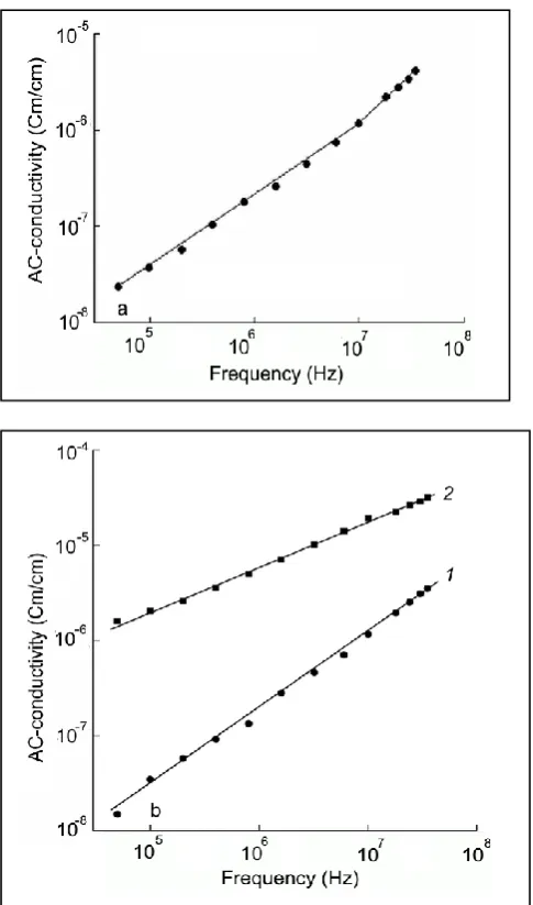
Figure 6 displays the frequency dependences of ac-conductivity for GaS (a) and GaSe (curve 1) and
0.2 0.8
S
GaSe
(b) (curve 2) single crystals at T = 300 K. The ac of GaS varies as f 0.8 in the frequency range 54 5
2 2 3
ln
96
)
(
f
f
a
kTN
e
f
F l phac
(7)where e is the electron charge, k is the Boltzmann constant, NF is the Fermi-level density of localized states, ɑ = 1 / is the localization radius ( is the decay constant of the wave function of localized charge carriers, ~ e–r), and ph is a phonon frequency.
Fig. 6.Frequency dependences of ac-conductivity for GaS (a), GaSe (1) and GaSe0.8S0.2 (b) (2) single crystals at T = 300 K
According to (7), ac conductivity varies as
.
ln
4
f
f
ph Therefore, at frequencies f ph ac isapproximately proportional to f0.8.
Using (7) and our experimental ac(f) data, we evaluated the Fermi-level density of states. For GaS and GaSe single crystal NF was determined to be 8.8 1018 eV–1 cm–3 and 9.3 1017 eV–1cm–3. The value of
ph in GaS is on the order of 1012 Hz. In the
F
N
calculations, the localization radius in GaSe was taken to be
a
l = 34 Å (the value determined experimentally for a GaSe single crystal from dc conductivity measurements).According to the theory of hopping conduction [9], the mean hop distance in an applied ac electric field is given by
,
ln
2
1
f
R
ph
(8)
where 1/f = is the mean hop time.
The R value calculated by (8) for GaS and GaSe single crystal is 87 Å and 187 Å. The mean hop time in GaS and GaSe is 2 10–7 s and 5.7 10-8 s respectively.
Using the relation (3) we evaluated the spread of the Fermi-level states in energy. We obtained for GaS and GaSe E = 0.08 eV. Same value for E was found also from dc-electric measurements of GaS single crystals.
From the relation
E
N
N
t
F
(9)we found the concentration of deep traps determining the ac conductivity of the GaSe crystals:
N
t = 7.3 1016 cm–3.IV. CONCLUSIONS
It is revealed that GaS single crystals exhibit a variable-range hopping conduction along a normal to their natural layers at temperatures T = 140–238 K in a dc- electric field. Ac-electric and dielectric properties of the
GaSe
1xS
x single crystals were studied in a broad frequency rangef
= 5 104 to 3.5 107 Hz. The nature of dielectric losses and the hopping mechanism of charge transport in theGaSe
1xS
x crystals were established, and the parameters of localized states in the forbidden gap of studied crystals have been evaluated from ac-electrical measurements.We have identified the nature of the dielectric loss and the hopping transport mechanism in ac electric fields and determined parameters of localized states in the band gap of the
GaSe
1xS
x crystals. Theexperimentally observed
ac ~f
0.8 behavior in the GaSe crystals is attributable to carrier hopping between localized states in the band gap of the crystals. Using our experimental
ac
f
data, we evaluated the Fermi-level density of states for the GaS and GaSe crystals,N
F= 6.2 1019 eV –1 cm –3 andF
Vol. 3 Issue 8, August - 2017 This value is about a factor of 6 greater than the
average distance between carrier localization centers in the crystals under investigation. Using this
R
value we evaluated the mean hop time of charge carriers in the GaSe crystals: = 5.7 10-8 s. We evaluated the spread of the Fermi-level states in energy for the GaS and GaSe crystals:
E
= 80 meV and found the concentration of deep traps determining the ac conductivity of the GaS and GaSe single crystals:N
t = 5 1018 cm-3 andt
N
= 7.3 1016 cm–3 respectively.REFERENCES
[1] S.N. Mustafaeva, M.M. Asadov, “Toki izotermicheskoy relaksatsii v kristallakh monosul'fida galliya, legirovannogo itterbiyem”, Neorganicheskiye materialy, (Moscow: in Russian) vol. 25, pp. 212-215, 1989. [“Currents of isothermal relaxation in yttrium-doped gallium monosulfide crystals”, Inorganic Materials], vol. 25, pp. 212-215, 1989.
[2] I.C.I. Terhell, “Polytypism in the III-VI layer compounds”, Prog. Cryst. Growth Charact. Mater., vol. 7, pp. 55-110, 1983.
[3] S.N. Mustafaeva, M.M. Asadov, “Currents of Isothermal Relaxation in GaS<Yb> Single Crystals”, Solid State Communications, vol. 45, pp. 491-494, 1983.
[4] S.N. Mustafaeva, M.M. Asadov, “Field Kinetics of Photocurrent in GaSe Amorphous Films”, Materials Chemistry and Physics, vol. 15, pp. 185-189, 1986.
[5] N.C. Fernelius, “Properties of gallium selenide single crystal”, Prog. Cryst. Growth and Charact., vol. 28, pp. 275-353, 1994.
[6] Y. Ni, H. Wu, C. Huang, M. Mao, Z. Wang, X. Cheng, “Growth and quality of gallium selenide (GaSe) crystals”, Journal of Crystal Growth, vol. 381, pp. 10-14, 2013.
[7] V.P. Vasilev, “Correlations between the Thermodynamic Properties of II–VI and III–VI Phases”, Inorganic Materials, vol. 43, pp. 115-124, 2007.
[8] S.N. Mustafaeva, “Dispersiya dielektricheskikh koeffitsiyentov i ac-provodimosti monokristallov TlGa1-xCoXS2 v radiochastotnom diapazone”, Zhurnal Radioelektroniki (Moscow: in Russian). N 4, pp.1-10, 2009. “Dispersion of the dielectric coefficients and ac conductivity of TlGa1-xCoXS2 single crystals in the radio-frequency range”, Journal of Radioelectronics. N 4, pp.1-10, 2009.
[9] N.F. Mott, E.A. Davis, Electron processes in noncrystalline materials, second ed., Oxford: Clarendon Press, 1979.
[10] V. Augelli, C. Manfredotti, R. Murri, R. Piccolo, L. Vasanelli, IL. Nuovo Cimento, “Anomalous impurity conductivity inn-GaSe andn-GaS”, B 38, pp. 327-336, 1977.
[11] B.I. Shklovsky, A. L. Efros, Electronic Properties of doped semiconductors, Springer-Verlag. Berlin Heidelberg, New York, Tokyo, 1984.