MMA8453Q Rev 4.1,08/2011
Freescale Semiconductor
Data Sheet: Technical Data
An Energy Efficient Solution by Freescale3-Axis,
10-bit/8-bit
Digital Accelerometer
The MMA8453Q is a smart low-power, three-axis, capacitive micromachined accelerometer with 10 bits of resolution. This accelerometer is packed with embedded functions with flexible user programmable options, configurable to two interrupt pins. Embedded interrupt functions allow for overall power savings relieving the host processor from continuously polling data.
The MMA8453Q has user selectable full scales of ±2g/±4g/±8g. The device can be configured to generate inertial wakeup interrupt signals from any combination of the configurable embedded functions allowing the MMA8453Q to monitor events and remain in a low power mode during periods of inactivity. The MMA8453Q is available in a 3 mm x 3 mm x 1 mm QFN package.
Features
• 1.95 V to 3.6 V supply voltage • 1.6 V to 3.6 V interface voltage
• ±2g/±4g/±8g dynamically selectable full-scale • Output Data Rates (ODR) from 1.56 Hz to 800 Hz • 99 μg/√Hz noise
• 10-bit and 8-bit digital output
• I2C digital output interface (operates to 2.25 MHz with 4.7 kΩ pullup) • Two programmable interrupt pins for six interrupt sources
• Three embedded channels of motion detection – Freefall or Motion Detection: 1 channel – Pulse Detection: 1 channel
– Jolt Detection: 1 channel
• Orientation (Portrait/Landscape) detection with set hysteresis
• Automatic ODR change for Auto-WAKE and return to SLEEP
• Self-Test
• RoHS compliant
• Current Consumption: 6 μA – 165 μA
Typical Applications
• eCompass applications
• Static orientation detection (Portrait/Landscape, Up/Down, Left/Right, Back/ Front position identification)
• Notebook, eReader and Laptop Tumble and Freefall Detection
• Real-time orientation detection (virtual reality and gaming 3D user position feedback)
• Real-time activity analysis (pedometer step counting, freefall drop detection for HDD, dead-reckoning GPS backup) • Motion detection for portable product power saving (Auto-SLEEP and Auto-WAKE for cell phone, PDA, GPS, gaming) • Shock and vibration monitoring (mechatronic compensation, shipping and warranty usage logging)
• User interface (menu scrolling by orientation change, tap detection for button replacement)
ORDERING INFORMATION
Part Number Temperature Range Package Description Shipping
MMA8453QT -40°C to +85°C QFN-16 Tray
MMA8453QR1 -40°C to +85°C QFN-16 Tape and Reel
16 PIN QFN 3 mm x 3 mm x 1 mm
CASE 2077-01
MMA8453Q
Top and Bottom View
Top View Pin Connections 1 2 3 4 5 9 10 11 12 13 14 15 16 8 7 6 NC VDD NC VDDIO BYP NC SCL GND NC GND INT1 GND INT2 SA 0 NC SDA
Contents
1 Block Diagram and Pin Description ... 3
1.1 Soldering Information ... 5
2 Mechanical and Electrical Specifications ... 6
2.1 Mechanical Characteristics ... 6
2.2 Electrical Characteristics ... 7
2.3 I2C Interface Characteristic ... 8
2.4 Absolute Maximum Ratings ... 9
3 Terminology ... 10 3.1 Sensitivity ... 10 3.2 Zero-g Offset ... 10 3.3 Self-Test ... 10 4 Modes of Operation ... 10 5 Functionality ... 11 5.1 Device Calibration ... 11
5.2 8-bit or 10-bit Data ... 11
5.3 Low Power Modes vs. High Resolution Modes ... 12
5.4 Auto-WAKE/SLEEP Mode ... 12
5.5 Freefall and Motion Detection ... 12
5.5.1 Freefall Detection ... 12
5.5.2 Motion Detection ... 12
5.6 Transient Detection ... 13
5.7 Tap Detection ... 13
5.8 Orientation Detection ... 13
5.9 Interrupt Register Configurations ... 15
5.10 Serial I2C Interface ... 15
5.10.1 I2C Operation ... 16
6 Register Descriptions ... 18
6.1 Data Registers ... 19
6.2 Portrait/Landscape Embedded Function Registers ... 24
6.3 Motion and Freefall Embedded Function Registers ... 26
6.4 Transient (HPF) Acceleration Detection ... 31
6.5 Single, Double and Directional Tap Detection Registers ... 33
6.6 Auto-WAKE/SLEEP Detection ... 37
6.7 Control Registers ... 38
Application Notes for Reference
The following is a list of Freescale Application Notes written for the MMA8451, 2, 3Q: •AN4068, Embedded Orientation Detection Using the MMA8451, 2, 3Q
•AN4069, Offset Calibration of the MMA8451, 2, 3Q
•AN4070, Motion and Freefall Detection Using the MMA8451, 2, 3Q
•AN4071, High Pass Data and Functions Using the MMA8451, 2,3Q
•AN4072, MMA8451, 2, 3Q Single/Double and Directional Tap Detection
•AN4073, Using the 32 Sample First In First Out (FIFO) in the MMA8451Q
•AN4074, Auto-Wake/Sleep Using the MMA8451, 2, 3Q
•AN4075, How Many Bits are Enough? The Trade-off Between High Resolution and Low Power Using Oversampling Modes
•AN4076, Data Manipulation and Basic Settings of the MMA8451, 2, 3Q
•AN4077, MMA8451, 2, 3Q Design Checklist and Board Mounting Guidelines
1
Block Diagram and Pin Description
Figure 1. Block Diagram
Figure 2. Direction of the Detectable Accelerations
10-bit SDA SCL I2C Embedded DSP Functions C to V Internal OSC Clock GEN ADC Converter VDDIO VSS X-axis Transducer Y-axis Transducer Z-axis Transducer Freefall and Motion Detection Transient Detection (i.e., fast motion,
jolt) Orientation with Set Hysteresis and Z-lockout Shake Detection through Motion Threshold Single, Double
Auto-WAKE/Auto-SLEEP Configurable with debounce counter and multiple motion interrupts for control
Auto-WAKE/SLEEP
ACTIVE Mode
SLEEP VDD
& Directional Tap Detection
INT1 INT2
MODE Options
Low Power Low Noise + Power High Resolution Normal
MODE Options
Low Power Low Noise + Power High Resolution Normal ACTIVE Mode WAKE 1 DIRECTION OF THE DETECTABLE ACCELERATIONS (BOTTOM VIEW) 5 9 13 X Y Z 1 (TOP VIEW) Earth Gravity
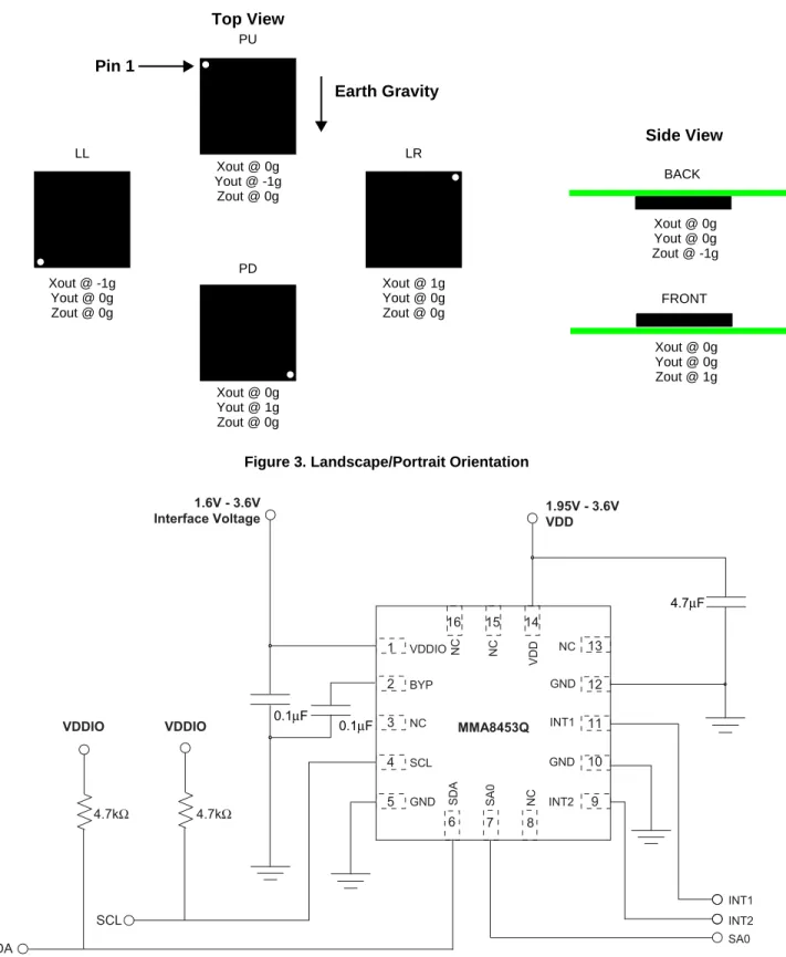
Figure 3 shows the device configuration in the 6 different orientation modes. These orientations are defined as the following: PU = Portrait Up, LR = Landscape Right, PD = Portrait Down, LL = Landscape Left, BACK and FRONT side views. There are several registers to configure the orientation detection and are described in detail in the register setting section.
Figure 3. Landscape/Portrait Orientation
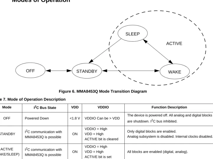
Top View PU Earth Gravity Pin 1 Xout @ 0g Yout @ -1g Zout @ 0g Xout @ 1g Yout @ 0g Zout @ 0g Xout @ 0g Yout @ 1g Zout @ 0g Xout @ -1g Yout @ 0g Zout @ 0g LL PD LR Side View FRONT Xout @ 0g Yout @ 0g Zout @ 1g BACK Xout @ 0g Yout @ 0g Zout @ -1g 0.1μF 1.6V - 3.6V Interface Voltage VDDIO VDDIO 4.7kΩ 4.7kΩ 1 GND VDDIO SCL NC INT2 INT1 GND GND SD A SA 0 VDD NC NC NC BYP NC MMA8453Q 2 16 12 13 14 15 11 10 3 4 5 6 7 8 9 4.7μF 0.1μF 1.95V - 3.6V VDD
The device power is supplied through VDD line. Power supply decoupling capacitors (100 nF ceramic plus 4.7 µF bulk, or a single 4.7 µF ceramic) should be placed as near as possible to the pins 1 and 14 of the device.
The control signals SCL, SDA, and SA0 are not tolerant of voltages more than VDDIO + 0.3 V. If VDDIO is removed, the control signals SCL, SDA, and SA0 will clamp any logic signals with their internal ESD protection diodes.
The functions, the threshold and the timing of the two interrupt pins (INT1 and INT2) are user programmable through the I2C interface. The SDA and SCL I2C connections are open drain and therefore require a pullup resistor as shown in the application diagram in Figure 4.
1.1
Soldering Information
The QFN package is compliant with the RoHS standard. Please refer to AN4077.
Table 1. Pin Description
Pin # Pin Name Description Pin Status
1 VDDIO Internal Power Supply (1.62 V - 3.6 V) Input 2 BYP Bypass capacitor (0.1 μF) Input 3 NC Leave open. Do not connect Open 4 SCL I2C Serial Clock Open Drain
5 GND Connect to Ground Input
6 SDA I2C Serial Data Open Drain 7 SA0 I2C Least Significant Bit of the Device I2C Address Input 8 NC Internally not connected (can be GND or VDD) Input 9 INT2 Inertial Interrupt 2 Output
10 GND Connect to Ground Input
11 INT1 Inertial Interrupt 1 Output
12 GND Connect to Ground Input
13 NC Internally not connected (can be GND or VDD) Input 14 VDD Power Supply (1.95 V - 3.6 V) Input 15 NC Internally not connected (can be GND or VDD) Input 16 NC Internally not connected (can be GND or VDD) Input
2
Mechanical and Electrical Specifications
2.1
Mechanical Characteristics
Table 2. Mechanical Characteristics @ VDD = 2.5 V, VDDIO = 1.8 V, T = 25°C unless otherwise noted.
Parameter Test Conditions Symbol Min Typ Max Unit
Measurement Range(1) FS[1:0] set to 00 2g Mode FS ±2 g FS[1:0] set to 01 4g Mode ±4 FS[1:0] set to 10 8g Mode ±8 Sensitivity FS[1:0] set to 00 2g Mode So 256 counts/g FS[1:0] set to 01 4g Mode 128 FS[1:0] set to 10 8g Mode 64
Sensitivity Accuracy(2) Soa ±2.5 %
Sensitivity Change vs. Temperature
FS[1:0] set to 00 2g Mode TCSo ±0.008 %/°C FS[1:0] set to 01 4g Mode FS[1:0] set to 10 8g Mode
Zero-g Level Offset Accuracy(3) FS[1:0] 2g, 4g, 8g TyOff ±20 mg
Zero-g Level Offset Accuracy Post Board Mount(4) FS[1:0] 2g, 4g, 8g TyOffPBM ±30 mg Zero-g Level Change vs. Temperature -40°C to 85°C TCOff ±0.15 mg/°C
Self-test Output Change(5) X Y Z FS[1:0] set to 00 4g Mode Vst +11 +16 +105 LSB ODR Accuracy 2 MHz Clock ±2 %
Output Data Bandwidth BW ODR/3 ODR/2 Hz
Output Noise Normal Mode ODR = 400 Hz Noise 126 µg/√Hz Output Noise Low Noise Mode(1) Normal Mode ODR = 400 Hz Noise 99 µg/√Hz
2.2
Electrical Characteristics
Table 3. Electrical Characteristics @ VDD = 2.5 V, VDDIO = 1.8 V, T = 25°C unless otherwise noted.
Parameter Test Conditions Symbol Min Typ Max Unit
Supply Voltage VDD(1)
1. There is no requirement for power supply sequencing. The VDDIO input voltage can be higher than the VDD input voltage.
1.95 2.5 3.6 V Interface Supply Voltage VDDIO(1) 1.62 1.8 3.6 V
Low Power Mode
ODR = 1.56 Hz IddLP 6 μA ODR = 6.25 Hz 6 ODR = 12.5 Hz 6 ODR = 50 Hz 14 ODR = 100 Hz 24 ODR = 200 Hz 44 ODR = 400 Hz 85 ODR = 800 Hz 165 Normal Mode ODR = 1.56 Hz Idd 24 μA ODR = 6.25 Hz 24 ODR = 12.5 Hz 24 ODR = 50 Hz 24 ODR = 100 Hz 44 ODR = 200 Hz 85 ODR = 400 Hz 165 ODR = 800 Hz 165
Current during Boot Sequence, 0.5 mSec max
duration using recommended Bypass Cap VDD = 2.5 V Idd Boot 1 mA Value of Capacitor on BYP pin -40°C 85°C Cap 75 100 470 nF STANDBY Mode Current @25°C VDD = 2.5 V, VDDIO = 1.8 V
STANDBY Mode IddStby 1.8 5 μA Digital High Level Input Voltage
SCL, SDA, SA0 VIH 0.75*VDDIO V
Digital Low Level Input Voltage
SCL, SDA, SA0 VIL 0.3*VDDIO V
High Level Output Voltage
INT1, INT2 IO = 500 μA VOH 0.9*VDDIO V
Low Level Output Voltage
INT1, INT2 IO = 500 μA VOL 0.1*VDDIO V
Low Level Output Voltage
SDA IO = 500 μA VOLS 0.1*VDDIO
V
Power on Ramp Time 0.001 1000 ms
Time from VDDIO on and VDD > Vmin until I2C
ready for operation Cbyp = 100 nF BT — 350 500 µs Turn-on time (STANDBY to ACTIVE) Ton 2/ODR + 1 ms s Turn-on time (Power Down to ACTIVE Mode) Ton 2/ODR + 2 ms s
2.3
I
2C Interface Characteristic
Table 4. I2C Slave Timing Values(1)1. All values referred to VIH (min) and VIL (max) levels.
Parameter Symbol I 2C Fast Mode Unit Min Max SCL Clock Frequency Pullup = 4.7 kΩ, Cb = 20 pF Pullup = 4.7 kΩ, Cb = 40 pF Pullup = 4.7 kΩ, Cb = 400 pF Pullup = 1 kΩ, Cb = 20 pF Pullup = 1 kΩ, Cb = 400 pF fSCL 0 0 0 0 0 2.250 100 Nonfunctional 4.50 750 MHz kHz — MHz kHz Bus Free Time between STOP and START Condition tBUF 1.3 μs
Repeated START Hold Time tHD;STA 0.6 μs
Repeated START Setup Time tSU;STA 0.6 μs
STOP Condition Setup Time tSU;STO 0.6 μs
SDA Data Hold Time(2)
2. tHD;DAT is the data hold time that is measured from the falling edge of SCL, applies to data in transmission and the acknowledge.
tHD;DAT 50 (3)
3. The maximum tHD;DAT could be 3.45 μs and 0.9 μs for Standard mode and Fast mode, but must be less than the maximum of tVD;DAT or tVD;ACK by a transition time.
μs SDA Valid Time (4)
4. tVD;DAT = time for Data signal from SCL LOW to SDA output (HIGH or LOW, depending on which one is worse).
tVD;DAT 0.9(3) μs
SDA Valid Acknowledge Time (5)
5. tVD;ACK = time for Acknowledgement signal from SCL LOW to SDA output (HIGH or LOW, depending on which one is worse).
tVD;ACK 0.9(3) μs
SDA Setup Time tSU;DAT 100(6)
6. A Fast mode I2C device can be used in a Standard mode I2C system, but the requirement tSU;DAT 250 ns must then be met. This will automatically be the case if the device does not stretch the LOW period of the SCL signal. If such a device does stretch the LOW period of the SCL signal, it must output the next data bit to the SDA line tr(max) + tSU;DAT = 1000 + 250 = 1250 ns (according to the Standard mode I2C
specification) before the SCL line is released. Also the acknowledge timing must meet this setup time
ns
SCL Clock Low Time tLOW 4.7 μs
SCL Clock High Time tHIGH 4 μs
SDA and SCL Rise Time tr 1000 ns
SDA and SCL Fall Time (7) (8)
7. Cb = total capacitance of one bus line in pF.
8. The maximum tf for the SDA and SCL bus lines is specified at 300 ns. The maximum fall time for the SDA output stage tf is specified at 250 ns. This allows series protection resistors to be connected in between the SDA and the SCL pins and the SDA/SCL bus lines without exceeding the maximum specified tf.
tf 300 ns
Figure 5. I2C Slave Timing Diagram
2.4
Absolute Maximum Ratings
Stresses above those listed as “absolute maximum ratings” may cause permanent damage to the device. Exposure to maximum rating conditions for extended periods may affect device reliability.
Table 5. Maximum Ratings
Rating Symbol Value Unit
Maximum Acceleration (all axes, 100 μs) gmax 5,000 g
Supply Voltage VDD -0.3 to + 3.6 V
Input voltage on any control pin (SA0, SCL, SDA) Vin -0.3 to VDDIO + 0.3 V
Drop Test Ddrop 1.8 m
Operating Temperature Range TOP -40 to +85 °C
Storage Temperature Range TSTG -40 to +125 °C
Table 6. ESD and Latchup Protection Characteristics
Rating Symbol Value Unit
Human Body Model HBM ±2000 V
Machine Model MM ±200 V
Charge Device Model CDM ±500 V
Latchup Current at T = 85°C — ±100 mA
This device is sensitive to mechanical shock. Improper handling can cause permanent damage of the part or cause the part to otherwise fail.
3
Terminology
3.1
Sensitivity
The sensitivity is represented in counts/g. In 2g mode the sensitivity is 256 counts/g. In 4g mode the sensitivity is 128 counts/ g and in 8g mode the sensitivity is 64 counts/g.
3.2
Zero-g Offset
Zero-g Offset (TyOff) describes the deviation of an actual output signal from the ideal output signal if the sensor is stationary. A sensor stationary on a horizontal surface will measure 0g in X-axis and 0g in Y-axis whereas the Z-axis will measure 1g. The output is ideally in the middle of the dynamic range of the sensor (content of OUT registers 0x00, data expressed as 2's complement number). A deviation from ideal value in this case is called Zero-g offset. Offset is to some extent a result of stress on the MEMS sensor and therefore the offset can slightly change after mounting the sensor onto a printed circuit board or exposing it to extensive mechanical stress.
3.3
Self-Test
Self-Test checks the transducer functionality without external mechanical stimulus. When Self-Test is activated, an electrostatic actuation force is applied to the sensor, simulating a small acceleration. In this case the sensor outputs will exhibit a change in their DC levels which are related to the selected full scale through the device sensitivity. When Self-Test is activated, the device output level is given by the algebraic sum of the signals produced by the acceleration acting on the sensor and by the electrostatic test-force.
4
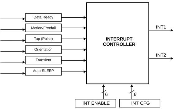
Modes of Operation
Figure 6. MMA8453Q Mode Transition Diagram Table 7. Mode of Operation Description
Mode I2C Bus State VDD VDDIO Function Description
OFF Powered Down <1.8 V VDDIO Can be > VDD The device is powered off. All analog and digital blocks are shutdown. I2C bus inhibited.
VDDIO = High SLEEP WAKE STANDBY OFF ACTIVE
5
Functionality
The MMA8453Q is a low-power, digital output 3-axis linear accelerometer with a I2C interface and embedded logic used to detect events and notify an external microprocessor over interrupt lines. The functionality includes the following:
• 8-bit or 10-bit data
• Four different oversampling options for compromising between resolution and current consumption based on application requirements
• Additional Low Noise mode that functions independently of the Oversampling modes for higher resolution • Low Power and Auto-WAKE/SLEEP for conservation of current consumption
• Single/Double tap with directional information 1 channel
• Motion detection with directional information or Freefall 1 channel
• Transient/Jolt detection based on a high pass filter and settable threshold for detecting the change in acceleration above a threshold with directional information 1 channel
• Portrait/Landscape detection with trip points fixed at 30° and 60° for smooth transitions between orientations.
All functionality is available in 2g, 4g or 8g dynamic ranges. There are many configuration settings for enabling all the different functions. Separate application notes have been provided to help configure the device for each embedded functionality.
5.1
Device Calibration
The device interface is factory calibrated for sensitivity and Zero-g offset for each axis. The trim values are stored in Non Volatile Memory (NVM). On power-up, the trim parameters are read from NVM and applied to the circuitry. In normal use, further calibration in the end application is not necessary. However, the MMA8453Q allows the user to adjust the Zero-g offset for each axis after power-up, changing the default offset values. The user offset adjustments are stored in six volatile registers. For more information on device calibration, refer to Freescale application note, AN4069.
5.2
8-bit or 10-bit Data
The measured acceleration data is stored in the OUT_X_MSB, OUT_X_LSB, OUT_Y_MSB, OUT_Y_LSB, OUT_Z_MSB, and OUT_Z_LSB registers as 2’s complement 10-bit numbers. The most significant 8-bits of each axis are stored in OUT_X (Y, Z)_MSB, so applications needing only 8-bit results can use these 3 registers and ignore OUT_X,Y, Z_LSB. To do this, the F_READ bit in CTRL_REG1 must be set. When the F_READ bit is cleared, the fast read mode is disabled.
When the full-scale is set to 2g, the measurement range is -2g to +1.9961g, and each count corresponds to 1g/256 (3.9 mg) at 10-bits resolution. When the full-scale is set to 8g, the measurement range is -8g to +7.9844g, and each count corresponds to 1g/64 (15.6 mg) at 10-bits resolution. The resolution is reduced by a factor of 4 if only the 8-bit results are used. For more information on the data manipulation between data formats and modes, refer to Freescale application note, AN4076. There is a device driver available that can be used with the Sensor Toolbox demo board (LFSTBEB8451, 2, 3Q) with this application note.
5.3
Low Power Modes vs. High Resolution Modes
The MMA8453Q can be optimized for lower power modes or for higher resolution of the output data. High resolution is achieved by setting the LNOISE bit in Register 0x2A. This improves the resolution but be aware that the dynamic range is limited to 4g when this bit is set. This will affect all internal functions and reduce noise. Another method for improving the resolution of the data is by oversampling. One of the oversampling schemes of the data can activated when MODS = 10 in Register 0x2B which will improve the resolution of the output data only. The highest resolution is achieved at 1.56 Hz.
There is a trade-off between low power and high resolution. Low Power can be achieved when the oversampling rate is reduced. When MODS = 11 the lowest power is achieved. The lowest power is achieved when the sample rate is set to 1.56 Hz. For more information on how to configure the MMA8453Q in Low Power mode or High Resolution mode and to realize the benefits, refer to Freescale application note, AN4075.
5.4
Auto-WAKE/SLEEP Mode
The MMA8453Q can be configured to transition between sample rates (with their respective current consumption) based on four of the interrupt functions of the device. The advantage of using the Auto-WAKE/SLEEP is that the system can automatically transition to a higher sample rate (higher current consumption) when needed but spends the majority of the time in the SLEEP mode (lower current) when the device does not require higher sampling rates. Auto-WAKE refers to the device being triggered by one of the interrupt functions to transition to a higher sample rate. This may also interrupt the processor to transition from a SLEEP mode to a higher power mode.
SLEEP mode occurs after the accelerometer has not detected an interrupt for longer than the user definable time-out period. The device will transition to the specified lower sample rate. It may also alert the processor to go into a lower power mode to save on current during this period of inactivity.
The Interrupts that can WAKE the device from SLEEP are the following: Tap Detection, Orientation Detection, Motion/Freefall, and Transient Detection. Refer to AN4074, for more detailed information for configuring the Auto-WAKE/SLEEP.
5.5
Freefall and Motion Detection
MMA8453Q has flexible interrupt architecture for detecting either a Freefall or a Motion. Freefall can be enabled where the set threshold must be less than the configured threshold, or motion can be enabled where the set threshold must be greater than the threshold. The motion configuration has the option of enabling or disabling a high pass filter to eliminate tilt data (static offset). The freefall does not use the high pass filter. For details on the Freefall and Motion detection with specific application examples and recommended configuration settings, refer to Freescale application note AN4070.
5.5.1
Freefall Detection
The detection of “Freefall” involves the monitoring of the X, Y, and Z axes for the condition where the acceleration magnitude is below a user specified threshold for a user definable amount of time. Normally the usable threshold ranges are between ±100 mg and ±500 mg.
5.5.2
Motion Detection
Motion is often used to simply alert the main processor that the device is currently in use. When the acceleration exceeds a set threshold the motion interrupt is asserted. A motion can be a fast moving shake or a slow moving tilt. This will depend on the threshold and timing values configured for the event. The motion detection function can analyze static acceleration changes or faster jolts. For example, to detect that an object is spinning, all three axes would be enabled with a threshold detection of > 2g. This condition would need to occur for a minimum of 100 ms to ensure that the event wasn't just noise. The timing value is set by a configurable debounce counter. The debounce counter acts like a filter to determine whether the condition exists for configurable set of time (i.e., 100 ms or longer). There is also directional data available in the source register to detect the direction of the motion. This is useful for applications such as directional shake or flick, which assists with the algorithm for various gesture detections.
5.6
Transient Detection
The MMA8453Q has a built-in high pass filter. Acceleration data goes through the high pass filter, eliminating the offset (DC) and low frequencies. The high pass filter cut-off frequency can be set by the user to four different frequencies which are dependent on the Output Data Rate (ODR). A higher cut-off frequency ensures the DC data or slower moving data will be filtered out, allowing only the higher frequencies to pass. The embedded Transient Detection function uses the high pass filtered data allowing the user to set the threshold and debounce counter. The transient detection feature can be used in the same manner as the motion detection by bypassing the high pass filter. There is an option in the configuration register to do this. This adds more flexibility to cover various customer use cases.
Many applications use the accelerometer’s static acceleration readings (i.e., tilt) which measure the change in acceleration due to gravity only. These functions benefit from acceleration data being filtered with a low pass filter where high frequency data is considered noise. However, there are many functions where the accelerometer must analyze dynamic acceleration. Functions such as tap, flick, shake and step counting are based on the analysis of the change in the acceleration. It is simpler to interpret these functions dependent on dynamic acceleration data when the static component has been removed. The Transient Detection function can be routed to either interrupt pin through bit 5 in CTRL_REG5 register (0x2E). Registers 0x1D – 0x20 are the dedicated Transient Detection configuration registers. The source register contains directional data to determine the direction of the acceleration, either positive or negative. For details on the benefits of the embedded Transient Detection function along with specific application examples and recommended configuration settings, please refer to Freescale application note, AN4071.
5.7
Tap Detection
The MMA8453Q has embedded single/double and directional tap detection. This function has various customizing timers for setting the pulse time width and the latency time between pulses. There are programmable thresholds for all three axes. The tap detection can be configured to run through the high pass filter and also through a low pass filter, which provides more customizing and tunable tap detection schemes. The status register provides updates on the axes where the event was detected and the direction of the tap. For more information on how to configure the device for tap detection please refer to Freescale application note AN4072.
5.8
Orientation Detection
The MMA8453Q has an orientation detection algorithm with the ability to detect all 6 orientations. The transition from portrait to landscape is fixed with a 45° threshold angle and a ±14° hysteresis angle. This allows the for a smooth transition from portrait to landscape at approximately 30° and then from landscape to portrait at approximately 60°.
The angle at which the device no longer detects the orientation change is referred to as the “Z-Lockout angle”. The device operates down to 29° from the flat position. All angles are accurate to ±2°.
For further information on the orientation detection function refer to Freescale application note, AN4068.
Figure 8 and Figure 9 show the definitions of the trip angles going from Landscape to Portrait and then also from Portrait to Landscape.
Figure 7. Landscape/Portrait Orientation
Top View PU Earth Gravity Pin 1 Xout @ 0g Yout @ -1g Zout @ 0g Xout @ 0g Yout @ 1g Zout @ 0g Xout @ -1g Yout @ 0g Zout @ 0g LL PD LR Side View FRONT Xout @ 0g Yout @ 0g Zout @ 1g BACK Xout @ 0g Yout @ 0g Zout @ -1g Xout @ 1g Yout @ 0g Zout @ 0g
Figure 8. Illustration of Landscape to Portrait Transition Figure 9. Illustration of Portrait to Landscape Transition Figure 10 illustrates the Z-angle lockout region. When lifting the device upright from the flat position it will be active for orientation detection as low as 29° from flat. .
Figure 10. Illustration of Z-Tilt Angle Lockout Transition PORTRAIT Landscape to Portrait 90° Trip Angle = 60° 0° Landscape PORTRAIT Portrait to Landscape 90° Trip Angle = 30° 0° Landscape UPRIGHT NORMAL 90° Z-LOCK = 29° 0° FLAT DETECTION REGION LOCKOUT REGION
5.9
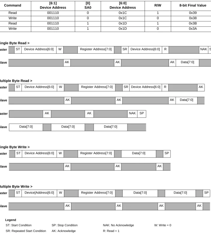
Interrupt Register Configurations
There aresix configurable interrupts in the MMA8453Q. These are Data Ready, Motion/Freefall, Tap (Pulse), Orientation, Transient, and Auto-SLEEP events. These six interrupt sources can be routed to one of two interrupt pins. The interrupt source must be enabled and configured. If the event flag is asserted because the event condition is detected, the corresponding interrupt pin, INT1 or INT2, will assert.
Figure 11. System Interrupt Generation Block Diagram
5.10
Serial I
2C Interface
Acceleration data may be accessed through an I2C interface thus making the device particularly suitable for direct interfacing with a microcontroller. The MMA8453Q features an interrupt signal which indicates when a new set of measured acceleration data is available thus simplifying data synchronization in the digital system that uses the device. The MMA8453Q may also be configured to generate other interrupt signals accordingly to the programmable embedded functions of the device for Motion, Freefall, Transient, Orientation, and Tap.
The registers embedded inside the MMA8453Q are accessed through the I2C serial interface (Table 8). To enable the I2C interface, VDDIO line must be tied high (i.e., to the interface supply voltage). If VDD is not present and VDDIO is present, the MMA8453Q is in off mode and communications on the I2C interface are ignored. The I2C interface may be used for
communications between other I2C devices and the MMA8453Q does not affect the I2C bus.
There are two signals associated with the I2C bus; the Serial Clock Line (SCL) and the Serial Data line (SDA). The latter is a bidirectional line used for sending and receiving the data to/from the interface. External pullup resistors connected to VDDIO are expected for SDA and SCL. When the bus is free both the lines are high. The I2C interface is compliant with Fast mode (400 kHz), and Normal mode (100 kHz) I2C standards (Table 4).
Table 8. Serial Interface Pin Description
Pin Name Pin Description
SCL I2C Serial Clock SDA I2C Serial Data
SA0 I2C least significant bit of the device address
INTERRUPT CONTROLLER Data Ready Motion/Freefall Tap (Pulse) Orientation Transient Auto-SLEEP
INT ENABLE INT CFG
INT1
INT2
5.10.1
I
2C Operation
The transaction on the bus is started through a start condition (START) signal. START condition is defined as a HIGH to LOW transition on the data line while the SCL line is held HIGH. After START has been transmitted by the Master, the bus is considered busy. The next byte of data transmitted after START contains the slave address in the first 7 bits, and the eighth bit tells whether the Master is receiving data from the slave or transmitting data to the slave. When an address is sent, each device in the system compares the first seven bits after a start condition with its address. If they match, the device considers itself addressed by the Master. The 9th clock pulse, following the slave address byte (and each subsequent byte) is the acknowledge (ACK). The transmitter must release the SDA line during the ACK period. The receiver must then pull the data line low so that it remains stable low during the high period of the acknowledge clock period.
A LOW to HIGH transition on the SDA line while the SCL line is high is defined as a stop condition (STOP). A data transfer is always terminated by a STOP. A Master may also issue a repeated START during a data transfer. The MMA8453Q expects repeated STARTs to be used to randomly read from specific registers.
The MMA8453Q's standard slave address is a choice between the two sequential addresses 0011100 and 0011101. The selection is made by the high and low logic level of the SA0 (pin 7) input respectively. The slave addresses are factory programmed and alternate addresses are available at customer request. The format is shown in Table 9.
Single Byte Read
The MMA8453Q has an internal ADC that can sample, convert and return sensor data on request. The transmission of an 8-bit command begins on the falling edge of SCL. After the eight clock cycles are used to send the command, note that the data returned is sent with the MSB first once the data is received. Figure 12shows the timing diagram for the accelerometer 8-bit I2C read operation. The Master (or MCU) transmits a start condition (ST) to the MMA8453Q, slave address ($1D), with the R/W bit set to “0” for a write, and the MMA8453Q sends an acknowledgement. Then the Master (or MCU) transmits the address of the register to read and the MMA8453Q sends an acknowledgement. The Master (or MCU) transmits a repeated start condition (SR) and then addresses the MMA8453Q ($1D) with the R/W bit set to “1” for a read from the previously selected register. The Slave then acknowledges and transmits the data from the requested register. The Master does not acknowledge (NAK) the transmitted data, but transmits a stop condition to end the data transfer.
Multiple Byte Read
When performing a multi-byte read or “burst read”, the MMA8453Q automatically increments the received register address commands after a read command is received. Therefore, after following the steps of a single byte read, multiple bytes of data can be read from sequential registers after each MMA8453Q acknowledgment (AK) is received until a no acknowledge (NAK) occurs from the Master followed by a stop condition (SP) signaling an end of transmission.
Single Byte Write
To start a write command, the Master transmits a start condition (ST) to the MMA8453Q, slave address ($1D) with the R/W bit set to “0” for a write, the MMA8453Q sends an acknowledgement. Then the Master (MCU) transmits the address of the register to write to, and the MMA8453Q sends an acknowledgement. Then the Master (or MCU) transmits the 8-bit data to write to the designated register and the MMA8453Q sends an acknowledgement that it has received the data. Since this transmission is complete, the Master transmits a stop condition (SP) to the data transfer. The data sent to the MMA8453Q is now stored in the appropriate register.
Table 9. I2C Address Selection Table
Slave Address (SA0 = 0) Slave Address (SA0 = 1) Comment
Multiple Byte Write
The MMA8453Q automatically increments the received register address commands after a write command is received. Therefore, after following the steps of a single byte write, multiple bytes of data can be written to sequential registers after each MMA8453Q acknowledgment (ACK) is received.
Figure 12. I2C Timing Diagram Table 10. I2C Device Address Sequence
Command [6:1]
Device Address
[0] SA0
[6:0]
Device Address R/W 8-bit Final Value
Read 001110 0 0x1C 1 0x39
Write 001110 0 0x1C 0 0x38
Read 001110 1 0x1D 1 0x3B
Write 001110 1 0x1D 0 0x3A
< Single Byte Read >
Master ST Device Address[6:0] W Register Address[7:0] SR Device Address[6:0] R NAK SP
Slave AK AK AK Data[7:0]
< Multiple Byte Read >
Master ST Device Address[6:0] W Register Address[7:0] SR Device Address[6:0] R AK
Slave AK AK AK Data[7:0]
Master AK AK NAK SP
Slave Data[7:0] Data[7:0] Data[7:0]
< Single Byte Write >
Master ST Device Address[6:0] W Register Address[7:0] Data[7:0] SP
Slave AK AK AK
< Multiple Byte Write >
Master ST Device[Address[6:0] W Register Address[7:0] Data[7:0] Data[7:0] SP
Slave AK AK AK AK
Legend
ST: Start Condition SP: Stop Condition NAK: No Acknowledge W: Write = 0 SR: Repeated Start Condition AK: Acknowledge R: Read = 1
6
Register Descriptions
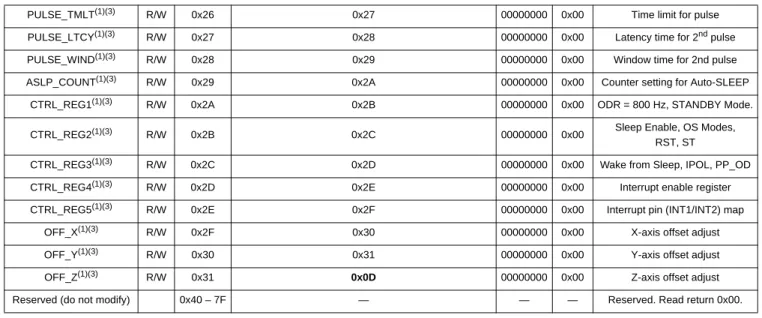
Table 11. Register Address MapName Type Register Address
Auto-Increment Address
Default Hex
Value Comment
F_READ=0 F_READ=1
STATUS(1)(2) R 0x00 0x01 00000000 0x00 Real time status
OUT_X_MSB(1)(2) R 0x01 0x02 0x03 Output — [7:0] are 8 MSBs of 10-bit sample.
OUT_X_LSB(1)(2) R 0x02 0x03 0x00 Output — [7:6] are 2 LSBs of 10-bit sample
OUT_Y_MSB(1)(2) R 0x03 0x04 0x05 Output — [7:0] are 8 MSBs of 10-bit sample
OUT_Y_LSB(1)(2) R 0x04 0x05 0x00 Output — [7:6] are 2 LSBs of 10-bit sample
OUT_Z_MSB(1)(2) R 0x05 0x06 0x00 Output — [7:0] are 8 MSBs of 10-bit sample
OUT_Z_LSB(1)(2) R 0x06 0x00 Output — [7:6] are 2 LSBs of 10-bit sample
Reserved R 0x07 — — — Reserved. Read return 0x00.
Reserved R 0x08 — — — Reserved. Read return 0x00.
SYSMOD(1)(2) R 0x0B 0x0C 00000000 0x00 Current System Mode
INT_SOURCE(1)(2) R 0x0C 0x0D 00000000 0x00 Interrupt status
WHO_AM_I(1) R 0x0D 0x0E 00111010 0x3A Device ID (0x3A)
XYZ_DATA_CFG(1)(3) R/W 0x0E 0x0F 00000000 0x00 Dynamic Range Settings
HP_FILTER_CUTOFF(1)(3) R/W 0x0F 0x10 00000000 0x00 Cut-off frequency is set to 16 Hz
@ 800 Hz
PL_STATUS(1)(2) R 0x10 0x11 00000000 0x00 Landscape/Portrait orientation
status
PL_CFG(1)(3) R/W 0x11 0x12 10000000 0x80 Landscape/Portrait configuration.
PL_COUNT(1)(3) R 0x12 0x13 00000000 0x00 Landscape/Portrait debounce
counter
PL_BF_ZCOMP(1)(3) R 0x13 0x14 01000100 0x44 Back-Front, Z-Lock Trip threshold
P_L_THS_REG(1)(3) R/W 0x14 0x15 10000100 0x84 Portrait to Landscape Trip Angle is
29°
FF_MT_CFG(1)(3) R/W 0x15 0x16 00000000 0x00 Freefall/Motion functional block
configuration
FF_MT_SRC(1)(2) R 0x16 0x17 00000000 0x00 Freefall/Motion event source
register
FF_MT_THS(1)(3) R/W 0x17 0x18 00000000 0x00 Freefall/Motion threshold register
FF_MT_COUNT(1)(3) R/W 0x18 0x19 00000000 0x00 Freefall/Motion debounce counter
Reserved R 0x19 — — — Reserved. Read return 0x00.
Reserved R 0x1A — — — Reserved. Read return 0x00.
Reserved R 0x1B — — — Reserved. Read return 0x00.
Note: Auto-increment addresses which are not a simple increment are highlighted in bold. The auto-increment addressing is only enabled when device registers are read using I2C burst read mode. Therefore the internal storage of the auto-increment address is cleared whenever a stop-bit is detected.
6.1
Data Registers
The following are the data registers for the MMA8453Q. For more information on data manipulation of the MMA8453Q, refer to application note, AN4076.
PULSE_TMLT(1)(3) R/W 0x26 0x27 00000000 0x00 Time limit for pulse
PULSE_LTCY(1)(3) R/W 0x27 0x28 00000000 0x00 Latency time for 2nd pulse
PULSE_WIND(1)(3) R/W 0x28 0x29 00000000 0x00 Window time for 2nd pulse
ASLP_COUNT(1)(3) R/W 0x29 0x2A 00000000 0x00 Counter setting for Auto-SLEEP
CTRL_REG1(1)(3) R/W 0x2A 0x2B 00000000 0x00 ODR = 800 Hz, STANDBY Mode.
CTRL_REG2(1)(3) R/W 0x2B 0x2C 00000000 0x00 Sleep Enable, OS Modes,
RST, ST
CTRL_REG3(1)(3) R/W 0x2C 0x2D 00000000 0x00 Wake from Sleep, IPOL, PP_OD
CTRL_REG4(1)(3) R/W 0x2D 0x2E 00000000 0x00 Interrupt enable register
CTRL_REG5(1)(3) R/W 0x2E 0x2F 00000000 0x00 Interrupt pin (INT1/INT2) map
OFF_X(1)(3) R/W 0x2F 0x30 00000000 0x00 X-axis offset adjust
OFF_Y(1)(3) R/W 0x30 0x31 00000000 0x00 Y-axis offset adjust
OFF_Z(1)(3) R/W 0x31 0x0D 00000000 0x00 Z-axis offset adjust
Reserved (do not modify) 0x40 – 7F — — — Reserved. Read return 0x00.
1. Register contents are preserved when transition from ACTIVE to STANDBY mode occurs. 2. Register contents are reset when transition from STANDBY to ACTIVE mode occurs.
3. Modification of this register’s contents can only occur when device is STANDBY mode except CTRL_REG1 ACTIVE bit and CTRL_REG2 RST bit.
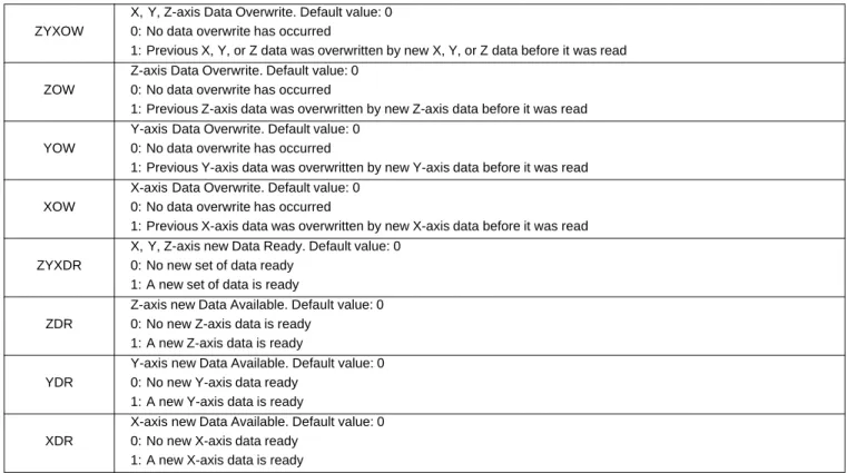
0x00 STATUS: Data Status Register (Read Only)
Bit 7 Bit 6 Bit 5 Bit 4 Bit 3 Bit 2 Bit 1 Bit 0
ZYXOW ZOW YOW XOW ZYXDR ZDR YDR XDR
ZYXOW is set whenever a new acceleration data is produced before completing the retrieval of the previous set. This event occurs when the content of at least one acceleration data register (i.e., OUT_X, OUT_Y, OUT_Z) has been overwritten. ZYXOW is cleared when the high-bytes of the acceleration data (OUT_X_MSB, OUT_Y_MSB, OUT_Z_MSB) of all the active channels are read.
ZOW is set whenever a new acceleration sample related to the Z-axis is generated before the retrieval of the previous sample. When this occurs the previous sample is overwritten. ZOW is cleared anytime OUT_Z_MSB register is read.
YOW is set whenever a new acceleration sample related to the Y-axis is generated before the retrieval of the previous sample. When this occurs the previous sample is overwritten. YOW is cleared anytime OUT_Y_MSB register is read.
XOW is set whenever a new acceleration sample related to the X-axis is generated before the retrieval of the previous sample. When this occurs the previous sample is overwritten. XOW is cleared anytime OUT_X_MSB register is read.
ZYXDR signals that a new sample for any of the enabled channels is available. ZYXDR is cleared when the high-bytes of the acceleration data (OUT_X_MSB, OUT_Y_MSB, OUT_Z_MSB) of all the enabled channels are read.
ZDR is set whenever a new acceleration sample related to the Z-axis is generated. ZDR is cleared anytime OUT_Z_MSB register is read.
YDR is set whenever a new acceleration sample related to the Y-axis is generated. YDR is cleared anytime OUT_Y_MSB register is read.
XDR is set whenever a new acceleration sample related to the X-axis is generated. XDR is cleared anytime OUT_X_MSB register is read.
Table 12. STATUS Description
ZYXOW
X, Y, Z-axis Data Overwrite. Default value: 0 0: No data overwrite has occurred
1: Previous X, Y, or Z data was overwritten by new X, Y, or Z data before it was read
ZOW
Z-axis Data Overwrite. Default value: 0 0: No data overwrite has occurred
1: Previous Z-axis data was overwritten by new Z-axis data before it was read
YOW
Y-axis Data Overwrite. Default value: 0 0: No data overwrite has occurred
1: Previous Y-axis data was overwritten by new Y-axis data before it was read
XOW
X-axis Data Overwrite. Default value: 0 0: No data overwrite has occurred
1: Previous X-axis data was overwritten by new X-axis data before it was read
ZYXDR
X, Y, Z-axis new Data Ready. Default value: 0 0: No new set of data ready
1: A new set of data is ready
ZDR
Z-axis new Data Available. Default value: 0 0: No new Z-axis data is ready
1: A new Z-axis data is ready
YDR
Y-axis new Data Available. Default value: 0 0: No new Y-axis data ready
1: A new Y-axis data is ready
XDR
X-axis new Data Available. Default value: 0 0: No new X-axis data ready
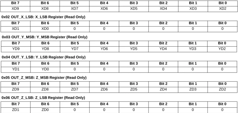
Data Registers: 0x01 OUT_X_MSB, 0x02 OUT_X_LSB, 0x03 OUT_Y_MSB, 0x04 OUT_Y_LSB, 0x05 OUT_Z_MSB, 0x06 OUT_Z_LSB
These registers contain the X-axis, Y-axis, and Z-axis 10-bit output sample data expressed as 2's complement numbers. The sample data output registers store the current sample data.
OUT_X_MSB, OUT_X_LSB, OUT_Y_MSB, OUT_Y_LSB, OUT_Z_MSB, and OUT_Z_LSB are stored in the
auto-incrementing address range of 0x01 to 0x06 to reduce reading the status followed by 10-bit axis data to 7 bytes. If the F_READ bit is set (0x2A bit 1), auto increment will skip over LSB registers. This will shorten the data acquisition from
7 bytes to 4 bytes. The LSB registers can only be read immediately following the read access of the corresponding MSB register. A random read access to the LSB registers is not possible. Reading the MSB register and then the LSB register in sequence ensures that both bytes (LSB and MSB) belong to the same data sample, even if a new data sample arrives between reading the MSB and the LSB byte.
0x0B: SYSMOD System Mode Register
The System mode register indicates the current device operating mode. Applications using the Auto-SLEEP/WAKE mechanism should use this register to synchronize the application with the device operating mode transitions.
0x01 OUT_X_MSB: X_MSB Register (Read Only)
Bit 7 Bit 6 Bit 5 Bit 4 Bit 3 Bit 2 Bit 1 Bit 0
XD9 XD8 XD7 XD6 XD5 XD4 XD3 XD2
0x02 OUT_X_LSB: X_LSB Register (Read Only)
Bit 7 Bit 6 Bit 5 Bit 4 Bit 3 Bit 2 Bit 1 Bit 0
XD1 XD0 0 0 0 0 0 0
0x03 OUT_Y_MSB: Y_MSB Register (Read Only)
Bit 7 Bit 6 Bit 5 Bit 4 Bit 3 Bit 2 Bit 1 Bit 0
YD9 YD8 YD7 YD6 YD5 YD4 YD3 YD2
0x04 OUT_Y_LSB: Y_LSB Register (Read Only)
Bit 7 Bit 6 Bit 5 Bit 4 Bit 3 Bit 2 Bit 1 Bit 0
YD1 YD0 0 0 0 0 0 0
0x05 OUT_Z_MSB: Z_MSB Register (Read Only)
Bit 7 Bit 6 Bit 5 Bit 4 Bit 3 Bit 2 Bit 1 Bit 0
ZD9 ZD8 ZD7 ZD6 ZD5 ZD4 ZD3 ZD2
0x06 OUT_Z_LSB: Z_LSB Register (Read Only)
Bit 7 Bit 6 Bit 5 Bit 4 Bit 3 Bit 2 Bit 1 Bit 0
ZD1 ZD0 0 0 0 0 0 0
0x0B SYSMOD: System Mode Register (Read Only)
Bit 7 Bit 6 Bit 5 Bit 4 Bit 3 Bit 2 Bit 1 Bit 0
0 0 0 0 0 0 SYSMOD1 SYSMOD0
Table 13. SYSMOD Description
SYSMOD[1:0]
System Mode. Default value: 00. 00: STANDBY mode
01: WAKE mode 10: SLEEP mode
0x0C: INT_SOURCE System Interrupt Status Register
In the interrupt source register the status of the various embedded features can be determined. The bits that are set (logic ‘1’) indicate which function has asserted an interrupt and conversely the bits that are cleared (logic ‘0’) indicate which function has not asserted or has de-asserted an interrupt. The bits are set by a low to high transition and are cleared by reading the appropriate interrupt source register. The SRC_DRDY bit is cleared by reading the X, Y and Z data. It is not cleared by simply reading the Status Register (0x00).
0x0C INT_SOURCE: System Interrupt Status Register (Read Only)
Bit 7 Bit 6 Bit 5 Bit 4 Bit 3 Bit 2 Bit 1 Bit 0
SRC_ASLP 0 SRC_TRANS SRC_LNDPRT SRC_PULSE SRC_FF_MT 0 SRC_DRDY
Table 14. INT_SOURCE Description
INT_SOURCE Description
SRC_ASLP
Auto-SLEEP/WAKE interrupt status bit. Default value: 0.
Logic ‘1’ indicates that an interrupt event that can cause a WAKE to SLEEP or SLEEP to WAKE system mode transition has occurred.
Logic ‘0’ indicates that no WAKE to SLEEP or SLEEP to WAKE system mode transition interrupt event has occurred.
WAKE to SLEEP transition occurs when no interrupt occurs for a time period that exceeds the user specified limit (ASLP_COUNT). This causes the system to transition to a user specified low ODR setting.
SLEEP to WAKE transition occurs when the user specified interrupt event has woken the system; thus causing the system to transition to a user specified high ODR setting.
Reading the SYSMOD register clears the SRC_ASLP bit.
SRC_TRANS
Transient interrupt status bit. Default value: 0.
Logic ‘1’ indicates that an acceleration transient value greater than user specified threshold has occurred. Logic ‘0’ indicates that no transient event has occurred.
This bit is asserted whenever “EA” bit in the TRANS_SRC is asserted and the interrupt has been enabled. This bit is cleared by reading the TRANS_SRC register.
SRC_LNDPRT
Landscape/Portrait Orientation interrupt status bit. Default value: 0.
Logic ‘1’ indicates that an interrupt was generated due to a change in the device orientation status. Logic ‘0’ indicates that no change in orientation status was detected.
This bit is asserted whenever “NEWLP” bit in the PL_STATUS is asserted and the interrupt has been enabled. This bit is cleared by reading the PL_STATUS register.
SRC_PULSE
Pulse interrupt status bit. Default value: 0.
Logic ‘1’ indicates that an interrupt was generated due to single and/or double pulse event. Logic ‘0’ indicates that no pulse event was detected.
This bit is asserted whenever “EA” bit in the PULSE_SRC is asserted and the interrupt has been enabled. This bit is cleared by reading the PULSE_SRC register.
SRC_FF_MT
Freefall/Motion interrupt status bit. Default value: 0.
Logic ‘1’ indicates that the Freefall/Motion function interrupt is active. Logic ‘0’ indicates that no Freefall or Motion event was detected.
This bit is asserted whenever “EA” bit in the FF_MT_SRC register is asserted and the FF_MT interrupt has been enabled.
This bit is cleared by reading the FF_MT_SRC register.
SRC_DRDY
Data Ready Interrupt bit status. Default value: 0.
Logic ‘1’ indicates that the X, Y, Z data ready interrupt is active indicating the presence of new data and/or data overrun. Otherwise if it is a logic ‘0’ the X, Y, Z interrupt is not active.
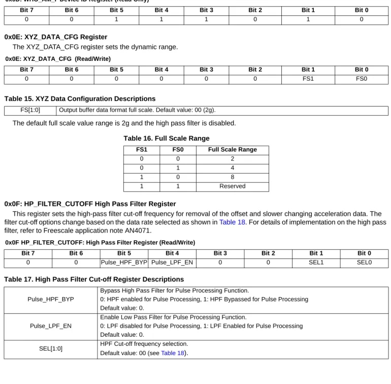
0x0D: WHO_AM_I Device ID Register
The device identification register identifies the part. The default value is 0x3A. This value is factory programmed. Consult the factory for custom alternate values.
0x0E: XYZ_DATA_CFG Register
The XYZ_DATA_CFG register sets the dynamic range.
The default full scale value range is 2g and the high pass filter is disabled.
0x0F: HP_FILTER_CUTOFF High Pass Filter Register
This register sets the high-pass filter cut-off frequency for removal of the offset and slower changing acceleration data. The filter cut-off options change based on the data rate selected as shown in Table 18. For details of implementation on the high pass filter, refer to Freescale application note AN4071.
0x0D: WHO_AM_I Device ID Register (Read Only)
Bit 7 Bit 6 Bit 5 Bit 4 Bit 3 Bit 2 Bit 1 Bit 0
0 0 1 1 1 0 1 0
0x0E: XYZ_DATA_CFG (Read/Write)
Bit 7 Bit 6 Bit 5 Bit 4 Bit 3 Bit 2 Bit 1 Bit 0
0 0 0 0 0 0 FS1 FS0
Table 15. XYZ Data Configuration Descriptions
FS[1:0] Output buffer data format full scale. Default value: 00 (2g).
Table 16. Full Scale Range
FS1 FS0 Full Scale Range
0 0 2
0 1 4
1 0 8
1 1 Reserved
0x0F HP_FILTER_CUTOFF: High Pass Filter Register (Read/Write)
Bit 7 Bit 6 Bit 5 Bit 4 Bit 3 Bit 2 Bit 1 Bit 0
0 0 Pulse_HPF_BYP Pulse_LPF_EN 0 0 SEL1 SEL0
Table 17. High Pass Filter Cut-off Register Descriptions
Pulse_HPF_BYP
Bypass High Pass Filter for Pulse Processing Function.
0: HPF enabled for Pulse Processing, 1: HPF Bypassed for Pulse Processing Default value: 0.
Pulse_LPF_EN
Enable Low Pass Filter for Pulse Processing Function.
0: LPF disabled for Pulse Processing, 1: LPF Enabled for Pulse Processing Default value: 0.
SEL[1:0] HPF Cut-off frequency selection. Default value: 00 (see Table 18).
6.2
Portrait/Landscape Embedded Function Registers
For more details on the meaning of the different user configurable settings and for example code refer to Freescale application note AN4068.
0x10: PL_STATUS Portrait/Landscape Status Register
This status register can be read to get updated information on any change in orientation by reading Bit 7, or on the specifics of the orientation by reading the other bits. For further understanding of Portrait Up, Portrait Down, Landscape Left, Landscape Right, Back and Front orientations please refer to Figure 3. The interrupt is cleared when reading the PL_STATUS register.
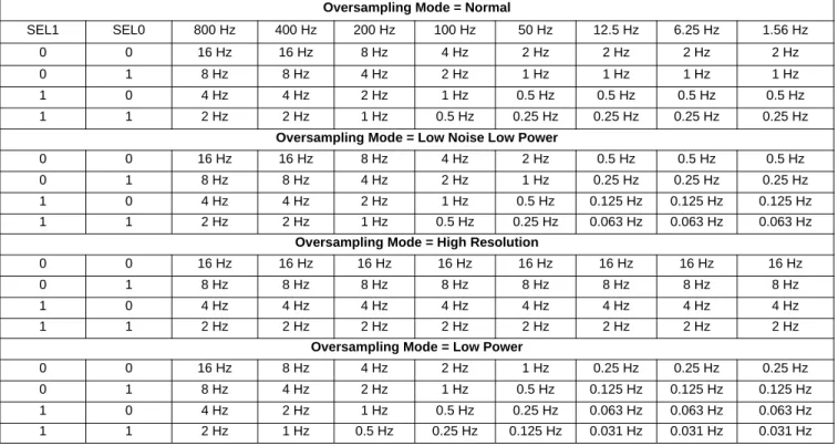
Table 18. High Pass Filter Cut-off Options
Oversampling Mode = Normal
SEL1 SEL0 800 Hz 400 Hz 200 Hz 100 Hz 50 Hz 12.5 Hz 6.25 Hz 1.56 Hz 0 0 16 Hz 16 Hz 8 Hz 4 Hz 2 Hz 2 Hz 2 Hz 2 Hz 0 1 8 Hz 8 Hz 4 Hz 2 Hz 1 Hz 1 Hz 1 Hz 1 Hz 1 0 4 Hz 4 Hz 2 Hz 1 Hz 0.5 Hz 0.5 Hz 0.5 Hz 0.5 Hz 1 1 2 Hz 2 Hz 1 Hz 0.5 Hz 0.25 Hz 0.25 Hz 0.25 Hz 0.25 Hz
Oversampling Mode = Low Noise Low Power
0 0 16 Hz 16 Hz 8 Hz 4 Hz 2 Hz 0.5 Hz 0.5 Hz 0.5 Hz 0 1 8 Hz 8 Hz 4 Hz 2 Hz 1 Hz 0.25 Hz 0.25 Hz 0.25 Hz 1 0 4 Hz 4 Hz 2 Hz 1 Hz 0.5 Hz 0.125 Hz 0.125 Hz 0.125 Hz 1 1 2 Hz 2 Hz 1 Hz 0.5 Hz 0.25 Hz 0.063 Hz 0.063 Hz 0.063 Hz
Oversampling Mode = High Resolution
0 0 16 Hz 16 Hz 16 Hz 16 Hz 16 Hz 16 Hz 16 Hz 16 Hz 0 1 8 Hz 8 Hz 8 Hz 8 Hz 8 Hz 8 Hz 8 Hz 8 Hz 1 0 4 Hz 4 Hz 4 Hz 4 Hz 4 Hz 4 Hz 4 Hz 4 Hz 1 1 2 Hz 2 Hz 2 Hz 2 Hz 2 Hz 2 Hz 2 Hz 2 Hz
Oversampling Mode = Low Power
0 0 16 Hz 8 Hz 4 Hz 2 Hz 1 Hz 0.25 Hz 0.25 Hz 0.25 Hz 0 1 8 Hz 4 Hz 2 Hz 1 Hz 0.5 Hz 0.125 Hz 0.125 Hz 0.125 Hz 1 0 4 Hz 2 Hz 1 Hz 0.5 Hz 0.25 Hz 0.063 Hz 0.063 Hz 0.063 Hz 1 1 2 Hz 1 Hz 0.5 Hz 0.25 Hz 0.125 Hz 0.031 Hz 0.031 Hz 0.031 Hz
0x10 PL_STATUS Register (Read Only)
Bit 7 Bit 6 Bit 5 Bit 4 Bit 3 Bit 2 Bit 1 Bit 0
NEWLP LO 0 0 0 LAPO[1] LAPO[0] BAFRO
Table 19. PL_STATUS Register Description
NEWLP Landscape/Portrait status change flag. Default value: 0.
0: No change, 1: BAFRO and/or LAPO and/or Z-Tilt lockout value has changed
LO
Z-Tilt Angle Lockout. Default value: 0. 0: Lockout condition has not been detected.
1: Z-Tilt lockout trip angle has been exceeded. Lockout has been detected. Landscape/Portrait orientation. Default value: 00
0x11 Portrait/Landscape Configuration Register
This register enables the Portrait/Landscape function and sets the behavior of the debounce counter.
0x12 Portrait/Landscape Debounce Counter
This register sets the debounce count for the orientation state transition. The minimum debounce latency is determined by the data rate set by the product of the selected system ODR and PL_COUNT registers. Any transition from WAKE to SLEEP or vice versa resets the internal Landscape/Portrait debounce counter. Note: The debounce counter weighting (time step) changes based on the ODR and the Oversampling mode. Table 22 explains the time step value for all sample rates and all Oversampling modes.
0x13: PL_BF_ZCOMP Back/Front and Z Compensation Register
The Z-Lock angle compensation is set to 29°. The Back to Front trip angle is set to ±75°.
Note: All angles are accurate to ±2°.
0x11 PL_CFG Register (Read/Write)
Bit 7 Bit 6 Bit 5 Bit 4 Bit 3 Bit 2 Bit 1 Bit 0
DBCNTM PL_EN 0 0 0 0 0 0
Table 20. PL_CFG Description
DBCNTM
Debounce counter mode selection. Default value: 1
0: Decrements debounce whenever condition of interest is no longer valid. 1: Clears counter whenever condition of interest is no longer valid.
PL_EN
Portrait/Landscape Detection Enable. Default value: 0 0: Portrait/Landscape Detection is Disabled.
1: Portrait/Landscape Detection is Enabled.
0x12 PL_COUNT Register (Read/Write)
Bit 7 Bit 6 Bit 5 Bit 4 Bit 3 Bit 2 Bit 1 Bit 0
DBNCE[7] DBNCE[6] DBNCE[5] DBNCE[4] DBNCE[3] DBNCE[2] DBNCE[1] DBNCE[0]
Table 21. PL_COUNT Description
DBCNE[7:0] Debounce Count value. Default value: 0000_0000.
Table 22. PL_COUNT Relationship with the ODR
ODR (Hz) Max Time Range (s) Time Step (ms)
Normal LPLN HighRes LP Normal LPLN HighRes LP
800 0.319 0.319 0.319 0.319 1.25 1.25 1.25 1.25 400 0.638 0.638 0.638 0.638 2.5 2.5 2.5 2.5 200 1.28 1.28 0.638 1.28 5 5 2.5 5 100 2.55 2.55 0.638 2.55 10 10 2.5 10 50 5.1 5.1 0.638 5.1 20 20 2.5 20 12.5 5.1 20.4 0.638 20.4 20 80 2.5 80 6.25 5.1 20.4 0.638 40.8 20 80 2.5 160 1.56 5.1 20.4 0.638 40.8 20 80 2.5 160
0x13: PL_BF_ZCOMP Register (Read Only)
Bit 7 Bit 6 Bit 5 Bit 4 Bit 3 Bit 2 Bit 1 Bit 0
BKFR[1] BKFR[0] 0 0 0 ZLOCK[2] ZLOCK[1] ZLOCK[0]
Table 23. PL_BF_ZCOMP Description
BKFR[7:6] Back Front Trip Angle Fixed Threshold = 01which is ≥ ±75°. ZLOCK[2:0] Z-Lock Angle Fixed Threshold = 100 which is 29°.
0x14: P_L_THS_REG Portrait/Landscape Threshold and Hysteresis Register
This register represents the Portrait to Landscape trip threshold.
:
6.3
Motion and Freefall Embedded Function Registers
The freefall/motion function can be configured in either Freefall or Motion Detection mode via the OAE configuration bit (0x15 bit 6). The freefall/motion detection block can be disabled by setting all three bits ZEFE, YEFE, and XEFE to zero.
Depending on the register bits ELE (0x15 bit 7) and OAE (0x15 bit 6), each of the freefall and motion detection block can operate in four different modes:
Mode 1: Freefall Detection with ELE = 0, OAE = 0
In this mode, the EA bit (0x16 bit 7) indicates a freefall event after the debounce counter is complete. The ZEFE, YEFE, and XEFE control bits determine which axes are considered for the freefall detection. Once the EA bit is set, and DBCNTM = 0, the EA bit can get cleared only after the delay specified by FF_MT_COUNT. This is because the counter is in decrement mode. If DBCNTM = 1, the EA bit is cleared as soon as the freefall condition disappears, and will not be set again before the delay specified by FF_MT_COUNT has passed. Reading the FF_MT_SRC register does not clear the EA bit. The event flags (0x16) ZHE, ZHP, YHE, YHP, XHE, and XHP reflect the motion detection status (i.e. high g event) without any debouncing, provided that the corresponding bits ZEFE, YEFE, and/or XEFE are set.
Mode 2: Freefall Detection with ELE = 1, OAE = 0
In this mode, the EA event bit indicates a freefall event after the debounce counter. Once the debounce counter reaches the time value for the set threshold, the EA bit is set, and remains set until the FF_MT_SRC register is read. When the FF_MT_SRC register is read, the EA bit and the debounce counter are cleared and a new event can only be generated after the delay specified by FF_MT_CNT. The ZEFE, YEFE, and XEFE control bits determine which axes are considered for the freefall detection. While EA = 0, the event flags ZHE, ZHP, YHE, YHP, XHE, and XHP reflect the motion detection status (i.e., high g event) without any debouncing, provided that the corresponding bits ZEFE, YEFE, and/or XEFE are set. The event flags ZHE, ZHP, YHE, YHP, XHE, and XHP are latched when the EA event bit is set. The event flags ZHE, ZHP, YHE, YHP, XHE, and XHP will start changing only after the FF_MT_SRC register has been read.
Mode 3: Motion Detection with ELE = 0, OAE = 1
In this mode, the EA bit indicates a motion event after the debounce counter time is reached. The ZEFE, YEFE, and XEFE control bits determine which axes are taken into consideration for motion detection. Once the EA bit is set, and DBCNTM = 0, the EA bit can get cleared only after the delay specified by FF_MT_COUNT. If DBCNTM = 1, the EA bit is cleared as soon as the motion high g condition disappears. The event flags ZHE, ZHP, YHE, YHP, XHE, and XHP reflect the motion detection status
0x14: P_L_THS_REG Register (Read Only)
Bit 7 Bit 6 Bit 5 Bit 4 Bit 3 Bit 2 Bit 1 Bit 0
P_L_THS[4] P_L_THS[3] P_L_THS[2] P_L_THS[1] P_L_THS[0] HYS[2] HYS[1] HYS[0]
Table 24. P_L_THS_REG Description
P_L_THS[7:3] Portrait/Landscape Fixed Threshold angle = 1_0000 (45°).
HYS[2:0] This is a fixed angle added to the threshold angle for a smoother transition from Portrait to Landscape and Landscape to Portrait. This angle is fixed at ±14°, which is 100.
Table 25. Trip Angles with Hysteresis for 45° Angle
Hysteresis Register Value Hysteresis ± Angle Range Landscape to Portrait Trip Angle Portrait to Landscape Trip Angle
0x15 FF_MT_CFG Freefall/Motion Configuration Register
This is the Freefall/Motion configuration register for setting up the conditions of the freefall or motion function.
OAE bit allows the selection between Motion (logical OR combination) and Freefall (logical AND combination) detection.
ELE denotes whether the enabled event flag will to be latched in the FF_MT_SRC register or the event flag status in the FF_MT_SRC will indicate the real-time status of the event. If ELE bit is set to a logic ‘1’, then the event flags are frozen when the EA bit gets set, and are cleared by reading the FF_MT_SRC source register.
ZHFE, YEFE, XEFE enable the detection of a motion or freefall event when the measured acceleration data on X, Y, Z channel is beyond the threshold set in FF_MT_THS register. If the ELE bit is set to logic ‘1’ in the FF_MT_CFG register new event flags are blocked from updating the FF_MT_SRC register.
FF_MT_THS is the threshold register used to detect freefall motion events. The unsigned 7-bit FF_MT_THS threshold register holds the threshold for the freefall detection where the magnitude of the X and Y and Z acceleration values is lower or equal than the threshold value. Conversely, the FF_MT_THS also holds the threshold for the motion detection where the magnitude of the X or Y or Z acceleration value is higher than the threshold value.
Figure 13. FF_MT_CFG High and Low g Level 0x16 FF_MT_SRC Freefall/Motion Source Register
0x15 FF_MT_CFG Register (Read/Write)
Bit 7 Bit 6 Bit 5 Bit 4 Bit 3 Bit 2 Bit 1 Bit 0
ELE OAE ZEFE YEFE XEFE 0 0 0
Table 26. FF_MT_CFG Description
ELE
Event Latch Enable: Event flags are latched into FF_MT_SRC register. Reading of the FF_MT_SRC register clears the event flag EA and all FF_MT_SRC bits. Default value: 0.
0: Event flag latch disabled; 1: event flag latch enabled
OAE
Motion detect / Freefall detect flag selection. Default value: 0. (Freefall Flag) 0: Freefall Flag (Logical AND combination)
1: Motion Flag (Logical OR combination) ZEFE Event flag enable on Z Default value: 0.
0: event detection disabled; 1: raise event flag on measured acceleration value beyond preset threshold YEFE Event flag enable on Y event. Default value: 0.
0: Event detection disabled; 1: raise event flag on measured acceleration value beyond preset threshold XEFE Event flag enable on X event. Default value: 0.
0: event detection disabled; 1: raise event flag on measured acceleration value beyond preset threshold
0x16: FF_MT_SRC Freefall and Motion Source Register (Read Only)
Bit 7 Bit 6 Bit 5 Bit 4 Bit 3 Bit 2 Bit 1 Bit 0
EA 0 ZHE ZHP YHE YHP XHE XHP
+8g
High g + Threshold (Motion)
Low g Threshold (Freefall)
High g - Threshold (Motion)
-8g X, Y, Z High g Region X, Y, Z High g Region X, Y, Z Low g Region Negative Positive Acceleration Acceleration
This register keeps track of the acceleration event which is triggering (or has triggered, in case of ELE bit in FF_MT_CFG register being set to 1) the event flag. In particular EA is set to a logic ‘1’ when the logical combination of acceleration events flags specified in FF_MT_CFG register is true. This bit is used in combination with the values in INT_EN_FF_MT and INT_CFG_FF_MT register bits to generate the freefall/motion interrupts.
An X,Y, or Z motion is true when the acceleration value of the X or Y or Z channel is higher than the preset threshold value defined in the FF_MT_THS register.
Conversely an X, Y, and Z low event is true when the acceleration value of the X and Y and Z channel is lower than or equal to the preset threshold value defined in the FF_MT_THS register.
0x17: FF_MT_THS Freefall and Motion Threshold Register
The threshold resolution is 0.063g/LSB and the threshold register has a range of 0 to 127 counts. The maximum range is to 8g. Note that even when the full scale value is set to 2g or 4g the motion detects up to 8g. If the Low Noise bit is set in Register 0x2A then the maximum threshold will be limited to 4g regardless of the full scale range.
DBCNTM bit configures the way in which the debounce counter is reset when the inertial event of interest is momentarily not true.
Table 27. Freefall/Motion Source Description
EA
Event Active Flag. Default value: 0.
0: No event flag has been asserted; 1: one or more event flag has been asserted.
See the description of the OAE bit to determine the effect of the 3-axis event flags on the EA bit.
ZHE
Z Motion Flag. Default value: 0.
0: No Z Motion event detected, 1: Z Motion has been detected This bit reads always zero if the ZEFE control bit is set to zero
ZHP
Z Motion Polarity Flag. Default value: 0.
0: Z event was Positive g, 1: Z event was Negative g This bit read always zero if the ZEFE control bit is set to zero
YHE
Y Motion Flag. Default value: 0.
0: No Y Motion event detected, 1: Y Motion has been detected This bit read always zero if the YEFE control bit is set to zero
YHP
Y Motion Polarity Flag. Default value: 0
0: Y event detected was Positive g, 1: Y event was Negative g This bit reads always zero if the YEFE control bit is set to zero
XHE
X Motion Flag. Default value: 0
0: No X Motion event detected, 1: X Motion has been detected This bit reads always zero if the XEFE control bit is set to zero
XHP
X Motion Polarity Flag. Default value: 0
0: X event was Positive g, 1: X event was Negative g This bit reads always zero if the XEFE control bit is set to zero
0x17 FF_MT_THS Register (Read/Write)
Bit 7 Bit 6 Bit 5 Bit 4 Bit 3 Bit 2 Bit 1 Bit 0
DBCNTM THS6 THS5 THS4 THS3 THS2 THS1 THS0
Table 28. FF_MT_THS Description
DBCNTM Debounce counter mode selection. Default value: 0.
0: increments or decrements debounce, 1: increments or clears counter. THS[6:0] Freefall /Motion Threshold: Default value: 000_0000.
0x18 FF_MT_COUNT Debounce Register
This register sets the number of debounce sample counts for the event trigger.
This register sets the minimum number of debounce sample counts of continuously matching the detection condition user selected for the freefall, motion event.
When the internal debounce counter reaches the FF_MT_COUNT value a Freefall/Motion event flag is set. The debounce counter will never increase beyond the FF_MT_COUNT value. Time step used for the debounce sample count depends on the ODR chosen and the Oversampling mode as shown in Table 30.
0x18 FF_MT_COUNT_Register (Read/Write)
Bit 7 Bit 6 Bit 5 Bit 4 Bit 3 Bit 2 Bit 1 Bit 0
D7 D6 D5 D4 D3 D2 D1 D0
Table 29. FF_MT_COUNT Description
D[7:0] Count value. Default value: 0000_0000
Table 30. FF_MT_COUNT Relationship with the ODR
ODR (Hz) Max Time Range (s) Time Step (ms)
Normal LPLN HighRes LP Normal LPLN HighRes LP
800 0.319 0.319 0.319 0.319 1.25 1.25 1.25 1.25 400 0.638 0.638 0.638 0.638 2.5 2.5 2.5 2.5 200 1.28 1.28 0.638 1.28 5 5 2.5 5 100 2.55 2.55 0.638 2.55 10 10 2.5 10 50 5.1 5.1 0.638 5.1 20 20 2.5 20 12.5 5.1 20.4 0.638 20.4 20 80 2.5 80 6.25 5.1 20.4 0.638 40.8 20 80 2.5 160 1.56 5.1 20.4 0.638 40.8 20 80 2.5 160
Figure 14. DBCNTM Bit Function High g Event on Count Threshold FF FFEA all 3-axis (Motion Detect) Counter Value High g Event on Count Threshold Debounce (a) all 3-axis (Motion Detect) Counter Value High g Event on Count Threshold Debounce EA all 3-axis (Motion Detect) Counter Value DBCNTM = 1 (b) EA DBCNTM = 0 (c)
6.4
Transient (HPF) Acceleration Detection
For more information on the uses of the transient function please review application note AN4071. This function is similar to the motion detection except that high pass filtered data is compared. There is an option to disable the high pass filter through the function. In this case the behavior is the same as the motion detection. This allows for the device to have 2 motion detection functions.
0x1D: Transient_CFG Register
The transient detection mechanism can be configured to raise an interrupt when the magnitude of the high pass filtered acceleration threshold is exceeded. The TRANSIENT_CFG register is used to enable the transient interrupt generation mechanism for the 3 axes (X, Y, Z) of acceleration. There is also an option to bypass the high pass filter. When the high pass filter is bypassed, the function behaves similar to the motion detection.
0x1E TRANSIENT_SRC Register
The Transient Source register provides the status of the enabled axes and the polarity (directional) information. When this register is read it clears the interrupt for the transient detection. When new events arrive while EA = 1, additional *TRANSE bits may get set, and the corresponding *_Trans_Pol flag become updated. However no *TRANSE bit may get cleared before the TRANSIENT_SRC register is read.
When the EA bit gets set while ELE = 1, all other status bits get frozen at their current state. By reading the TRANSIENT_SRC register, all bits get cleared.
0x1D TRANSIENT_CFG Register (Read/Write)
Bit 7 Bit 6 Bit 5 Bit 4 Bit 3 Bit 2 Bit 1 Bit 0
0 0 0 ELE ZTEFE YTEFE XTEFE HPF_BYP
Table 31. TRANSIENT_CFG Description
ELE
Transient event flags are latched into the TRANSIENT_SRC register. Reading of the TRANSIENT_SRC register clears the event flag. Default value: 0.
0: Event flag latch disabled; 1: Event flag latch enabled
ZTEFE Event flag enable on Z transient acceleration greater than transient threshold event. Default value: 0.
0: Event detection disabled; 1: Raise event flag on measured acceleration delta value greater than transient threshold. YTEFE Event flag enable on Y transient acceleration greater than transient threshold event. Default value: 0.
0: Event detection disabled; 1: Raise event flag on measured acceleration delta value greater than transient threshold. XTEFE Event flag enable on X transient acceleration greater than transient threshold event. Default value: 0.
0: Event detection disabled; 1: Raise event flag on measured acceleration de