W&M ScholarWorks
W&M ScholarWorks
Arts & Sciences Articles
Arts and Sciences
2015
Modification of electronic structure in compressively strained
Modification of electronic structure in compressively strained
vanadium dioxide films
vanadium dioxide films
T. J. Huffman
College of William and Mary
Peng Xu
College of William and Mary
A. J. Hollingshad
College of William and Mary
M. M. Qazilbash
College of William and Mary
Lei Wang
College of William and Mary
See next page for additional authors
Follow this and additional works at: https://scholarworks.wm.edu/aspubs
Recommended Citation
Recommended Citation
Huffman, T. J., Xu, P., Hollingshad, A. J., Qazilbash, M. M., Wang, L., Lukaszew, R. A., ... & Wolf, S. A. (2015). Modification of electronic structure in compressively strained vanadium dioxide films. Physical Review B, 91(20), 205140.
This Article is brought to you for free and open access by the Arts and Sciences at W&M ScholarWorks. It has been accepted for inclusion in Arts & Sciences Articles by an authorized administrator of W&M ScholarWorks. For more information, please contact [email protected].
Authors
Authors
T. J. Huffman, Peng Xu, A. J. Hollingshad, M. M. Qazilbash, Lei Wang, R. A. Lukaszew, S. Kittiwatanakul, J. Lu, and S. A. Wolf
PHYSICAL REVIEW B91, 205140 (2015)
Modification of electronic structure in compressively strained vanadium dioxide films
T. J. Huffman,1Peng Xu,1A. J. Hollingshad,1M. M. Qazilbash,1,*Lei Wang,1R. A. Lukaszew,1S. Kittiwatanakul,2J. Lu,2and S. A. Wolf2,3
1Department of Physics, College of William and Mary, Williamsburg, Virginia 23187-8795, USA 2Department of Material Sciences and Engineering, University of Virginia, Charlottesville, Virginia 22904, USA
3Department of Physics, University of Virginia, Charlottesville, Virginia 22904, USA
(Received 23 July 2014; revised manuscript received 10 April 2015; published 29 May 2015) Vanadium dioxide (VO2) undergoes a phase transition between an insulating monoclinic phase and a conducting
rutile phase. Like other correlated electron systems, the properties of VO2 can be extremely sensitive to small
changes in external parameters such as strain. In this paper, we investigate a compressively strained VO2 film
grown on (001) quartz substrate in which the phase transition temperature (Tc) has been depressed to 325 K from
the bulk value of 340 K. Infrared and optical spectroscopy reveals that the lattice dynamics of this strained film are similar to unstrained VO2. However, some of the electronic interband transitions of the strained VO2film are
significantly shifted in energy from those in unstrained VO2. The lattice dynamics remain largely unchanged
while theTc and some of the electronic interband transitions differ substantially from the bulk values, which
highlights the role of electronic correlations in driving this metal-insulator phase transition.
DOI:10.1103/PhysRevB.91.205140 PACS number(s): 71.30.+h
I. INTRODUCTION
Strongly interacting degrees of freedom in condensed matter systems often lead to novel emergent properties such as metal-insulator transitions (MITs), superconductivity, colossal magnetoresistance, and high phase transition temperature (Tc)
superconductivity [1–4]. Because they arise from multiple strongly interacting degrees of freedom, these emergent properties are highly sensitive to external factors such as temperature, strain, chemical doping, and applied fields. The true potential of strongly correlated systems lies in this sensitivity to external parameters. With sufficient understand-ing, the properties of these materials could be engineered to match specific applications. The technological impact of harnessing these novel properties for applications cannot be overstated.
Additional experimental data are needed to further inform our understanding of these materials. Unfortunately, the same sensitivity to external parameters that makes these materials so promising for future applications makes experimental char-acterization difficult. The emergent properties can vary widely among different samples of the same material, as different growth techniques and conditions result in variations in strain, stoichiometry, and microstructure. Thus, for experimental measurements of these systems to provide meaningful insight, the external parameters, the intrinsic interacting degrees of freedom, and the resulting properties must all be well characterized. Hence, measurements on samples subject to external perturbations, for example, pressure and strain [5–10], can provide additional insight into the underlying physics of these systems.
Vanadium dioxide (VO2) is perhaps the canonical strongly
correlated transition metal oxide; its relatively simple unit cell and stoichiometric composition make it an ideal material to study strong correlations. Bulk VO2 undergoes a MIT at Tc=340 K between an insulating phase below the Tcand a
*Corresponding author: [email protected]
metallic phase above theTc. The MIT is accompanied by a
structural transition between the insulating monoclinic (M1)
lattice and the conducting rutile (tetragonal) lattice [Fig.1(a)]. Despite extensive research, the precise relationship between the lattice structure and the electronic properties remains elusive. As the vanadium atoms are in the 4+valence state, there is expected to be one electron in the vanadiumdorbitals. The crystal field of the oxygen octahedron splits the vanadium d orbitals into two higher energyeσ
g orbitals, which contain lobes pointing towards the oxygen atoms, and the remaining three lower energyt2gorbitals. Thet2gorbitals are additionally split into twoeπ
g and onea1g orbital. Thea1g band has lobes pointing along the rutilecr(M1aM) axis and is slightly lower in energy than theeπ
g band.
Early on, a simple scheme was proposed by Goodenough [11] to explain the role of the structural transition in the MIT in terms of the vanadium d orbitals. The structural change from rutile toM1 has two salient features: a dimerization of
the vanadium atoms along the rutilecr (aM) direction and an antiferroelectric type tilting of these vanadium dimers relative to the surrounding oxygen structure. Insulating behavior was proposed to arise as follows. The dimerization would lead to a splitting of thea1gorbitals into bonding (a1g) and antibonding (a1∗g) bands, while the antiferroelectric tilting of the vanadium pairs would lead to an upshift of theeπ
g orbitals away from the Fermi energy to produce a gap between the filled bondinga1g band and the emptyegπband [11]. This effective band structure scheme is qualitatively supported by experimental data on bulk crystals and thin films [12–14]. However, a precise quantitative understanding of how this scheme is realized—in particular, the roles of electronic correlations and the structural instability in the MIT—remains a matter of debate [15–18]. A complete understanding of this correlated system is necessary to predict and control the emergent properties as a function of external parameters.
Broadband infrared (IR) and optical spectroscopy is a powerful technique for investigating the MIT in VO2because
it provides insight into both the lattice and the electronic structure via the IR active phonons and the optical interband
T. J. HUFFMANet al. PHYSICAL REVIEW B91, 205140 (2015)
transitions, respectively. Previous IR and optical spectroscopy experiments have been performed on bulk VO2 and thin
films [12–14,19,20]. However, VO2 films grown on different
substrates and by different techniques can have significantly different strain states and microstructure. Because of the ex-treme sensitivity to external parameters in strongly correlated systems mentioned previously, accurate characterization of the strain and microstructure of various films, as well as the resultant emergent properties, can provide additional insight into the physics of these materials.
In this paper, we report the IR and optical properties of a VO2 film grown on a quartz substrate. The paper is
organized as follows. We start with a thorough description of our preliminary characterization of the sample and then describe the IR and optical spectroscopy experiments. Next, we report our results on the IR active phonons in theM1phase. We then report and discuss the strain induced changes of the electronic interband transitions in bothM1and rutile phases.
We conclude with a brief summary of important results and their implications. Technical details of the experiment and data analysis, as well as tabulated optical constants of the VO2film,
are presented in the Supplemental Material [21].
II. EXPERIMENTAL METHODS A. Sample characterization
The VO2 film used in this experiment is a 70 nm thick
VO2film on a 0.5 mm thick (001) quartz substrate. The film
was synthesized using the reactive biased target ion beam
deposition (RBTIBD) method [22]. The growth conditions for optimal stoichiometry are the same as those reported elsewhere [22,23]. An atomic force microscope image of the sample, shown in Fig.1(b), indicates that the VO2 film consists of
many individual grains with an in-plane size of ∼100 nm. X-ray diffraction shows that the individual VO2 grains are
oriented such that the (011) plane of theM1 phase is in the
plane of the substrate; see Fig.1(c)and [21]. This becomes the (110) plane in the rutile structure [21]. However, there is no preferred orientation of the grains with respect to rotations about the out of plane direction.
The first-order phase transition in this film exhibits the classic hysteresis usually observed in VO2. The temperature
dependent transmission through the VO2film-substrate system
at 0.5 eV provides a clear picture of the hysteresis loop for the MIT in this particular film [Fig. 1(d)]. The photon energy of 0.5 eV is just below that of the energy gap in insulating VO2, resulting in minimal absorption and high transmission
intensity. The transmission drops with the occurrence of metallicity in the vicinity of the MIT due to the increased reflectance and absorption of the metallic phase. TheTc of the film is depressed from the bulk Tc of 340 to 325 K.
The 15 K width of the hysteresis loop in this film is somewhat broader than what is seen in VO2 crystals [24].
Such broadening of the hysteresis and the phase transition is typical of polycrystalline VO2thin films because of variation
in grain size and strain inhomogeneity. This inhomogeneity is consistent with the width of the x-ray diffraction peak shown in Fig.1(c).
FIG. 1. (Color online) (a) Lattice structure of theM1and rutile phases of VO2. (b) Atomic force microscopy image at room temperature
showing the surface roughness and multigrain structure of the (011)M1VO2film on quartz substrate. (c) X-ray diffraction peak resulting from
the (011)M1lattice planes. The Gaussian fit and resulting full width at half maximum are shown. The peak positions for the bulk (011)M1
and analogous (110) rutile diffraction spots are shown as vertical lines. (d) Transmission through the sample at a photon energy of 0.5 eV, demonstrating the temperature dependence of the transition during heating and cooling runs. TheTconset of 325 K is significantly lower than
that of bulk crystals (340 K).
MODIFICATION OF ELECTRONIC STRUCTURE IN . . . PHYSICAL REVIEW B91, 205140 (2015)
B. Spectroscopic methods
Spectroscopic measurements were performed to study the optical properties of the VO2 film on quartz between
7.5 meV and 6.0 eV. This broad spectral range is necessary to characterize both the electronic and the lattice degrees of freedom. Specifically, temperature dependent spectroscopic ellipsometry was performed in the spectral range between 0.6 and 6.0 eV at temperatures of 300 and 360 K. The VO2is in the M1insulating phase at 300 K and in the rutile metallic phase
at 360 K. Due to its self-referencing nature, spectroscopic ellipsometry enables precise measurement of the complex dielectric function of the sample. To extend our spectral range into the far-IR, near-normal incidence reflectance between 7.5 meV and 1 eV was obtained at 300 and 360 K. In addition to the VO2 film on quartz, the same temperature
dependent spectroscopic measurements were performed on the (001) quartz substrate. In order to obtain the optical constants of the VO2 film, the ellipsometry and reflectance
data for the substrate and the VO2 film-substrate system
was fit with Kramers-Kronig consistent Drude, Lorentzian, Tauc-Lorentzian, and Gaussian oscillators. We report the optical constants of the VO2 film at 300 and 360 K in the
insulating and metallic phases, respectively. Spectra and fits, in addition to technical details about the modeling procedure, are included in the Supplemental Material [21].
III. RESULTS AND DISCUSSION A. Sample strain
In a polycrystalline thin film that is not lattice matched to the substrate, such as the one studied in this paper, the resultant strain state of the film is particularly dependent on the growth technique. Stresses occur between neighboring grains and have been shown to affect theTcof VO2[25]. Such strain is sensitive
to the grain size and film microstructure, and both these pro-perties are influenced by the growth conditions. There are additional factors present in sputtered films [26]. In a process referred to as “shot peening,” compressive strain arises as a result of the sample being bombarded by energetic particles during growth. Compressive in-plane strain in sputtered oxide films is often attributed to this effect [27,28]. Thermal strain from the mismatch of the coefficient of thermal expansion between the film and the substrate may also be present.
The out of plane strain can be calculated by comparing the measured x-ray diffraction data shown in Fig. 1(c)with the literature. X-ray diffraction shows that the (011)M1 plane
spacing is 3.23 ˚A in the present sample. From the literature, the (011)M1 plane spacing ranges from 3.1978 and 3.2067 ˚A
for bulk VO2[29,30]. Averaging the literature values implies a
tensile strain in the out of plane direction of 0.89%. This type of tensile strain would result from compressive strains in the plane of the substrate. The transition temperature for the MIT is expected to be most sensitive to strain along theaM (cr) direction [31]. Depression of theTcto 325 K, as is the case in
our film, has been seen in VO2nanorods with a compressive
strain of 1.5% along aM [10]. Similar strong dependence of theTcas a function of strain has been seen in VO2 films on
TiO2[32]. In both cases, compressive strain alongaMresults in depression of the transition temperature. Thus, it is reasonable
to conclude that the VO2 film we studied has a compressive
strain of∼1.5% alongaM.
TheaM axis contracts by∼1% across the phase transition into the rutile phase. This would tend to relax compressive strains along cr (aM) in the metallic phase. Some partial relaxation of the in-plane strain is evidenced by the shift of the x-ray diffraction peak towards the bulk rutile value shown in the Supplemental Material [21]. However, as the out of plane strain in the metallic phase is still tensile, the in-plane strain is still somewhat compressive. Additional changes to the strain as the sample is heated across the MIT could be induced due to the mismatch of thermal expansion coefficients between the VO2film and the quartz substrate. The
coefficients of thermal expansion ofarVO2,crVO2, anda
-axis quartz are 4×10⁻⁶/K, 25×10−6/K, and 16×10−6/K,
respectively [33,34]. Thus, this is at most a 0.1% effect over the 60 K temperature range investigated in this paper and has a negligible impact on the strain state of the film.
Here, we discuss the stoichiometry of the VO2 films we
have studied. One effect of oxygen deficiency is to reduce the Tc. However, oxygen deficiency also increases disorder in the film, which significantly reduces the jump in the dc conductivity across the MIT [23]. In the films we studied, the optical conductivity in the low frequency limit changes by four orders of magnitude across the MIT. This is consistent with stoichiometric VO2 with minimal oxygen deficiency,
comparable to single crystals. Moreover, we clearly see VO2 optical phonon features in the spectra, which is further
evidence that the film is composed of crystallites with minimal disorder due to oxygen deficiency. Hence, the reduction in the Tcin our films is due to compressive in-plane strain rather than oxygen deficiency.
B. IR active phonons and lattice dynamics
Due to the polycrystalline nature of the film, we measured the reflectance with unpolarized light. Thus, features due to IR active phonons of bothAuandBusymmetries are expected
to appear in the reflectance data in the insulatingM1 phase.
However, the relative strengths of each phonon will depend on the orientation of the dipole moment relative to the plane of the sample: Phonons with in-plane dipole moments will have a larger contribution to the effective optical constants [19,20]. The dipole moments of theAuphonon modes, which
lie parallel tobM, are at 45°out of the plane of the substrate in this film geometry. In contrast, theBu modes have dipole
moments in theaM −cM plane. Depending on the specificBu
mode in question, the dipole moments could be anywhere from 0°to 45°out of plane. Thus, all 15 IR active phonons should, in principle, contribute to the measured spectrum.
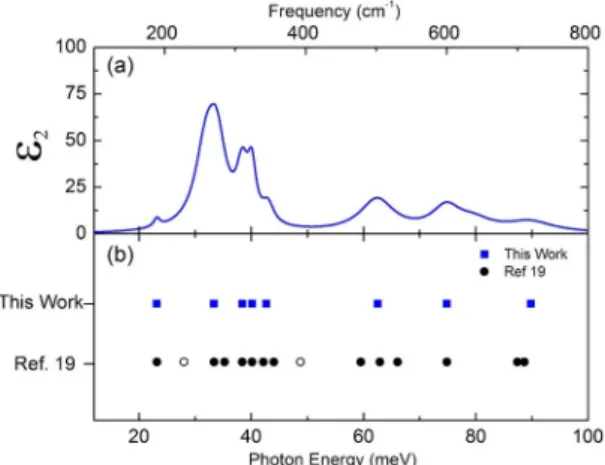
The measured imaginary part of the complex dielectric function in the phonon region of the VO2 film is shown in
Fig.2(a). We are able to resolve eight IR active phonons in this paper. The IR active phonons in VO2 crystals have been
previously characterized by optical spectroscopy [19,20]. It is not unusual that we resolve fewer than the expected 15 IR active phonons, as some VO2phonons overlap. Moreover, the
sample is a thin film, resulting in much weaker phonon features in comparison to those of the quartz substrate, which dominate the measured spectrum in this region. More importantly, the
T. J. HUFFMANet al. PHYSICAL REVIEW B91, 205140 (2015)
FIG. 2. (Color online) (a) Measured imaginary part of the com-plex dielectric function (ε2) of the VO2 film in the phonon region.
(b) The measured center frequencies of the IR active phonons of the VO2 film are compared to previous data taken on bulk crystals
[19]. Open circles denote phonon modes from Ref. [19] that are not obvious in the spectra measured in this paper (see text).
clearly resolved VO2phonon center frequencies differ from the
bulk values by at most 1.3% [Fig.2(b)]. Raman spectroscopy performed on films grown by the same method also shows negligible shift in the phonon center frequencies compared to bulk VO2[35]. Remarkably, the lattice dynamics are virtually
unchanged relative to bulk VO2 in a film where theTcis so
significantly depressed.
Previous experiments have seen that spectral features due to the rutile phase phonons are fairly weak and difficult to resolve from the metallic background [19,20]. In this paper, IR active phonon features in the rutile phase are not observed in the reflectance spectrum. Apart from the high conductivity of VO2 in the metallic phase, the absence of rutile phonon
features in this paper can be attributed to the thin film nature of the sample and strong phonon features of the quartz substrate.
C. Interband transitions and electronic structure
1. Assignment of spectral features
In the absence of polarization dependent data due to the polycrystalline nature of the film, features in the optical conductivity cannot be unambiguously assigned to specific interband transitions. However, energy scales of the measured spectral features can still be discussed within the context of band theoretical results on VO2 [36,37]. A schematic view
of the band structure of VO2 is shown in Fig.3 to support
the following discussion. The lower and upper Hubbard bands (LHB and UHB, respectively), which, in the rutile phase, arise from electronic correlations not considered by conventional band theory, are shown explicitly in Fig.3.
The measured optical conductivity for the rutile phase at 360 K is shown in Fig. 4(a). Some of the lower energy interband transitions in this compressively strained sample differ significantly from those measured previously on bulk VO2 and thin films [12–14,19]. The VO2 film on quartz
exhibits a broad Drude-like metallic response “q” and an interband transition “s,” which are consistent with previous papers. Feature s at 3.1 eV is attributed to transitions between
FIG. 3. (Color online) Schematic showing energy levels of the relevant vanadium and oxygen bands in the metallic and insulating states of VO2. The Fermi level is denoted asEF. The possible (partial) Hubbard splitting of thea1gband due to correlation effects in the rutile metal is shown explicitly.
the O2porbitals and the vanadiumeπg bands. However, in this strained VO2 film on quartz, we resolve additional features:
a pseudogap-type feature in the low frequency electronic response “p” and well-defined features “r” and “t” at 2.2 and 5 eV, respectively. The pseudogap-type feature p has been seen in a few previous papers [20,38]. Compressive strain alongcr is expected to lower the energy of thea1g band [11]. This is supported by x-ray emission spectroscopy experiments on strained VO2 films grown on TiO2 [39]. The slight lowering
of the filleda1g bands relative to theeπg bands could account for the prominence of the pseudogap-type feature p if this feature is due to optical transitions between those two bands. This lowering in energy of thea1g band, due to compressive strain, would increase the occupation of the bottom half of the a1gband. Increased occupation of thea1gband could lead to a reduction in screening and an increase in electronic correlation effects for electrons in thea1gbands, similar to the explanation presented by Zylbersztejn and Mott for the insulatingM1phase
[15].
Correlation effects in the rutile phase could lead to a degree of splitting of the a1g band into lower and upper Hubbard bands [40]. A “satellite” of thea1g band, consistent with this type of lower Hubbard band, has been seen previously in photoemission experiments on bulk VO2 [41]. We interpret
feature r as transitions from the filled parts of thea1g bands (both the unsplit portion and the lower Hubbard band) to the unfilled upper Hubbard band. Such splitting could also account for feature t if it is assigned to the transition between the O2p and the upper Hubbard bands. There is also likely some absorption near 5 eV due to transitions between the O2p and theeσ
g bands, as the O2p toeπg transition is seen at 3 eV and the crystal field splitting betweeneπ
g andegσ is expected to be on the order of 2 eV [42]. A well resolved feature at 5 eV is not present in theM1 phase, which supports the assignment
MODIFICATION OF ELECTRONIC STRUCTURE IN . . . PHYSICAL REVIEW B91, 205140 (2015)
FIG. 4. (Color online) (a) Optical conductivityσ1 for the rutile
(red) andM1(blue) phases as a function of photon energy. Phonons
have been subtracted from the conductivity of theM1phase and this
procedure has negligible impact on the calculation ofNeff. Spectral
features are denoted by lowercase and uppercase letters for the rutile andM1phases, respectively. The assignment of these spectral features
to specific interband transitions is discussed in the text. (b) The effective number of carriers per vanadium atom (see text).
of feature t to a transition involving the upper Hubbard bands, as these bands might be expected to shift more significantly across the MIT. In this scenario, the upper Hubbard band would need to lie at an energy close to that of theeσ
gbands. This would imply a correlation induced Hubbard splitting of a comparable magnitude to the crystal field splitting and is expected to be much larger than the splitting caused by a Peierl-type lattice distortion.
Increased correlations due to compressive strain, as dis-cussed above, would result in more states being shifted into the satellites of the a1g orbital and could account for why we are able to clearly resolve features r and t in this sample. It is also possible that correlation effects lead to significant splitting of thea1g bands even in the unstrained rutile phase. Subtle evidence of a transition between the Hubbard bands was seen previously in rutile VO2on sapphire near 3 eV [13].
However, this feature could not be clearly resolved from the O2p toegπ transition. Thus, it is also possible that this feature has been shifted to a lower energy in our particular film.
The measured optical conductivity for the M1 phase at
300 K is shown in Fig.4(a). Features “A” and “C” are consistent with previous papers [12–14]. Feature A is attributed to transitions between the filled bonding a1g and the empty egπ bands, while feature C is attributed to transitions between the filled O2pand the emptyeπg bands.
We observe an additional feature “B,” which is different from previous papers. While a strong feature at low energy,
∼0.9 eV, is seen in single crystals for light polarized
perpendicular toaM [12], feature B in the present paper is somewhat stronger and at a much higher energy, 1.9 eV. A similar strong feature at 1.9 eV is not seen in previous paper on thin films grown on sapphire and TiO2[13,14].
Interestingly, the transition betweena1ganda∗1g, which has been seen in previous experiments on bulk crystals and thin films around 2.5 eV [12,13], is not clearly present near this energy in VO2 on quartz data. It is likely that this transition
has been downshifted as a result of strain. It is possible that feature B is thea1g toa∗1g transition, having been shifted to lower energies in this particular film. Such an interpretation is not unreasonable, given that the analogous feature in the rutile, feature r, occurs at a similar energy to feature B. However, recent dynamical mean field theory (DMFT) calculations show that the splitting betweena1g anda1∗g should increase with compressive strain along theaMaxis [31]. Such an increase in splitting would result in a shift of thea1g toa1∗g transition to higher energies, into the vicinity of feature C. Indeed, there is fine structure in feature C that would be consistent with such an explanation.
The evidence for Hubbard bands in the rutile metal suggests that correlation effects are significant enough to govern the evolution of VO2 properties upon lowering temperature. In
Goodenough’s band theory picture [11], the antiferroelectric displacement of the vanadium atoms in the M1 structure is
necessary to raise the energy of theeπ
g bands above the Fermi energy to produce an energy gap. However, in both the present experiment and a previous paper [13], the O2ptoeπg transition is not shifted appreciably, certainly much less than the 0.6 eV band gap ofM1VO2. This could indicate that theeπg band is not as strongly dependent on the change in lattice symmetry as expected. Alternatively, the O2p bands may shift significantly across the phase transition.
2. Spectral weight transfer
As thef-sum rule is a fundamental statement of conserva-tion of charge in a material, it should be conserved across the MIT. The total spectral weight (Atotal) is conserved as follows.
The following equations employ Gaussian (cgs) units: Atotal≡ ∞ 0 σ1(ω)dω= nπ e2 2m0V (1) Here,σ1(ω) is the real part of the optical conductivity as a
function of photon energyω, nis the number of electrons in a volumeV of the material,eis the elementary charge, andm0 is the free electron mass. By integrating to a finite frequency, one can consider the spectral weight (A) below a certain photon energy (ωc):
A(ωc)=
ωc
0
σ1(ω)dω (2)
It is interesting to defineNeff, which in the spirit of Eqs. (1)
and (2), gives us theeffectivenumber of carriers with optical mass equal tom0that contribute to absorption below a certain
photon energyωc: Neff(ωc)= 2m0V π e2 ωc 0 σ1(ω)dω (3) 205140-5
T. J. HUFFMANet al. PHYSICAL REVIEW B91, 205140 (2015)
The effective number of carriers are shown in Fig. 4(b)
as a function of photon energy. The volumes used for this calculation are ½ of the rutile [33] and ¼ of the M1 [30]
unit cell volumes from the literature. This corresponds to the volume of a single formula unit and thus a single vanadium atom. While there are some slight shifts in spectral weight up to and exceeding 6 eV, 95% of the spectral weight has been recovered by 4 eV. The f-sum rule is still not fully satisfied at such high energies, which clearly indicates a rearrangement of the electronic structure at even higher energies. For example, feature t, clearly resolved in the rutile phase at 5 eV, is not present in the M1 phase. Such
rearrangement at higher energy scales supports the hypothesis that the MIT in VO2is electronically driven. Previous optical
spectroscopy measurements have also shown shifts in spectral weight across the MIT up to and exceeding 6 eV [13,14].
The spectral weight of the conduction electrons (features q and p) in the rutile phase will be largely contained below 1.8 eV in the broad Drude-like feature. While one might naively expect one conduction electron per vanadium atom, Neffat this energy is only 0.21. This indicates that the effective electron mass (m∗) of the conduction electrons is several times m0and/or that the spectral weight of the correlated vanadium
3delectrons has shifted to energies higher than 1.8 eV.
IV. CONCLUSIONS
The properties of strongly correlated condensed matter systems can change dramatically when subject to external perturbations such as strain. In the VO2 film on quartz
substrate investigated in this paper, compressive strain along theaM (cr) direction results in theTcbeing shifted down to
325 K from the bulkTcof 340 K. Broadband IR and optical spectroscopy was used to characterize both the electronic and the lattice-structural degrees of freedom in this film to elucidate the cause of this significant change in theTcand its
implications regarding the nature of the MIT in VO2.
Strain affects the interband transitions by altering the relative energies of the bands, as well as their orientation in real space. Such changes can have important implications in a correlated system where Coulomb repulsion between electrons, orbital overlaps, and screening play nontrivial roles. Some interband transitions in this strained VO2 film differ
significantly from those measured previously in bulk crystals and thin films. In particular, two new features are observed.
Features at 2.2 and 5.2 eV are observed in the rutile phase, which we attribute to transitions between the filled a1g and O2pstates and the upper Hubbard band. It is possible that these features are more prominent because the compressive strain alongcr increases the occupation of thea1g orbital relative toeπg, thereby reducing screening and enhancing correlation effects in thea1gband. A new feature is seen at∼1.9 eV in the M1 phase; the values ofε2 andσ1 are significantly higher at
this energy than in bulk crystals or other thin films. A definitive assignment of thea1gtoa1∗g optical interband transition is not possible at present, although there are two possible scenarios: Either it has been shifted down to 1.9 eV due to strain and appears as feature B, or it appears as a fine structure in feature C near 3 eV.
Interestingly, unlike the interband transitions, the IR active phonons in these strained films are similar to their bulk counterparts, indicating that the forces between the vanadium and the oxygen ions remain largely unchanged despite the strained nature of this film. Nevertheless, this strain is sufficient to cause significant changes in the transition temperature and the optical interband transitions. This would indicate that the Tc is more sensitive to changes in the orbital overlaps and
occupation than it is to changes in the lattice dynamics. It is reasonable to conclude that the MIT in VO2 is more likely
to be driven by changes in electronic correlations and orbital occupations rather than by lattice dynamics. The change in lattice structure could then occur as a consequence of the variations in electronic structure and interactions.
As the electronic and optical properties of VO2 are
incredibly sensitive to strain, this system has potential for applications for which strain engineering could be used to tune these properties. We have measured and documented the IR and optical properties of VO2film on quartz substrate. This
is a necessary step towards fully realizing the potential of strain engineering in this material.
ACKNOWLEDGMENTS
M.M.Q. is grateful for financial support from the National Science Foundation’s Division of Materials Research (Grant No. 1255156) and the Jeffress Memorial Trust (Grant No. J-1014). R.A.L., S.W., and J.L. also acknowledge support from the Nanoelectronics Research Initiative/Semiconductor Research Corp.-sponsored Virginia Nanoelectronics Center (Contract No. 2010-NE-2115) and the Commonwealth of Virginia through the Virginia Micro-Electronics Consortium.
[1] M. Imada, A. Fujimori, and Y. Tokura,Rev. Mod. Phys.70,1039
(1998).
[2] D. C. Johnston,Adv. Phys.59,803(2010).
[3] D. N. Basov, R. D. Averitt, D. van der Marel, M. Dressel, and K. Haule,Rev. Mod. Phys.83,471(2011).
[4] E. Dagotto,Science309,257(2005).
[5] E. Arcangeletti, L. Baldassarre, D. Di Castro, S. Lupi, L. Malavasi, C. Marini, A. Perucchi, and P. Postorino,Phys. Rev. Lett.98,196406(2007).
[6] C. Marini, E. Arcangeletti, D. Di Castro, L. Baldassare, A. Perucchi, S. Lupi, L. Malavasi, L. Boeri, E. Pomjakushina,
K. Conder, and P. Postorino, Phys. Rev. B 77, 235111
(2008).
[7] J. M. Atkin, S. Berweger, E. K. Chavez, M. B. Raschke, J. Cao, W. Fan, and J. Wu, Phys. Rev. B 85, 020101
(2012).
[8] N. B. Aetukuri, A. X. Gray, M. Drouard, M. Cossale, L. Gao, A. H. Reid, R. Kukreja, H. Ohldag, C. A. Jenkins, E. Arenholz, K. P. Roche, H. a. D¨urr, M. G. Samant, and S. S. P. Parkin,Nat. Phys.9,661(2013).
[9] J. H. Park, J. M. Coy, T. S. Kasirga, C. Huang, Z. Fei, S. Hunter, and D. H. Cobden,Nature500,431(2013).
MODIFICATION OF ELECTRONIC STRUCTURE IN . . . PHYSICAL REVIEW B91, 205140 (2015) [10] J. Cao, Y. Gu, W. Fan, L. Q. Chen, D. F. Ogletree, K. Chen,
N. Tamura, M. Kunz, C. Barrett, J. Seidel, and J. Wu,Nano Lett. 10,2667(2010).
[11] J. B. Goodenough,J. Solid State Chem.3,490(1971). [12] H. W. Verleur, A. S. Barker, and C. N. Berglund,Phys. Rev.
172,788(1968).
[13] M. M. Qazilbash, A. A. Schafgans, K. S. Burch, S. J. Yun, B. G. Chae, B. J. Kim, H. T. Kim, and D. N. Basov,Phys. Rev. B 77,115121(2008).
[14] K. Okazaki, S. Sugai, Y. Muraoka, and Z. Hiroi,Phys. Rev. B 73,165116(2006).
[15] A. Zylbersztejn and N. F. Mott,Phys. Rev. B11,4383(1975). [16] D. Paquet and P. Lerouxhugon,Phys. Rev. B22,5284(1980). [17] T. M. Rice, H. Launois, and J. P. Pouget,Phys. Rev. Lett.73,
3042(1994).
[18] J. P. Pouget, H. Launois, J. P. Dhaenens, P. Merenda, and T. M. Rice,Phys. Rev. Lett.35,873(1975).
[19] A. S. Barker, H. W. Verleur, and H. J. Guggenheim,Phys. Rev. Lett.17,1286(1966).
[20] T. J. Huffman, P. Xu, M. M. Qazilbash, E. J. Walter, H. Krakauer, J. Wei, D. H. Cobden, H. A. Bechtel, M. C. Martin, G. L. Carr, and D. N. Basov,Phys. Rev. B87,115121(2013).
[21] See Supplemental Material athttp://link.aps.org/supplemental/ 10.1103/PhysRevB.91.205140for technical details of the data analysis and tabulated optical constants.
[22] K. G. West, J. Lu, J. Yu, D. Kirkwood, W. Chen, Y. Pei, J. Claassen, and S. A. Wolf, J. Vac. Sci. Technol. A 26, 133
(2008).
[23] S. Kittiwatanakul, J. Laverock, D. Newby, K. E. Smith, S. A. Wolf, and J. Lu,J. Appl. Phys.114,053703(2013).
[24] B. S. Mun, K. Chen, J. Yoon, C. Dejoie, N. Tamura, M. Kunz, Z. Liu, M. E. Grass, S.-K. Mo, C. Park, Y. Y. Lee, and H. Ju,
Phys. Rev. B84,113109(2011).
[25] R. A. Aliev, V. N. Andreev, V. M. Kapralova, V. A. Klimov, A. I. Sobolev, and E. B. Shadrin, Phys. Solid State48, 929
(2006).
[26] H. Windischmann,Crit. Rev. Solid State Mater. Sci.17, 547
(1992).
[27] W. Y. Park, K. H. Ahn, and C. S. Hwang,Appl. Phys. Lett.83,
4387(2003).
[28] T. Ashida, K. Kato, H. Omoto, and A. Takamatsu,Jpn. J. Appl. Phys.49,065501(2010).
[29] G. Andersson,Acta Chem. Scand.10,623(1956).
[30] J. M. Longo and P. Kierkega,Acta Chem. Scand.24,420(1970). [31] B. Lazarovits, K. Kim, K. Haule, and G. Kotliar,Phys. Rev. B
81,115117(2010).
[32] Y. Muraoka, Y. Ueda, and Z. Hiroi,J. Phys. Chem. Solids63,
965(2002).
[33] D. B. Mcwhan, M. Marezio, J. P. Remeika, and P. D. Dernier,
Phys. Rev. B10,490(1974).
[34] A. H. Jay,Proc. R. Soc. London142,237(1933).
[35] E. Radue, E. Crisman, L. Wang, S. Kittiwatanakul, J. Lu, S. A. Wolf, R. Wincheski, R. A. Lukaszew, and I. Novikova,J. Appl. Phys.113,233104(2013).
[36] V. Eyert,Ann. Phys. (Leipzig)11,650(2002).
[37] S. Biermann, A. Poteryaev, A. I. Lichtenstein, and A. Georges,
Phys. Rev. Lett.94,026404(2005).
[38] M. M. Qazilbash, M. Brehm, B.-G. Chae, P.-C. Ho, G. O. Andreev, B.-J. Kim, S. J. Yun, A. V. Balatsky, M. B. Maple, F. Keilmann, H.-T. Kim, and D. N. Basov,Science318,1750
(2007).
[39] J. Laverock, L. F. J. Piper, A. R. H. Preston, B. Chen, J. McNulty, K. E. Smith, S. Kittiwatanakul, J. W. Lu, S. A. Wolf, P.-A. Glans, and J.-H. Guo,Phys. Rev. B85,081104(2012).
[40] S. Biermann, A. Georges, A. Lichtenstein, and T. Giamarchi,
Phys. Rev. Lett.87,276405(2001).
[41] T. C. Koethe, Z. Hu, M. W. Haverkort, C. Schuessler-Langeheine, F. Venturini, N. B. Brookes, O. Tjernberg, W. Reichelt, H. H. Hsieh, H.-J. Lin, C. T. Chen, and L. H. Tjeng,
Phys. Rev. Lett.97,116402(2006).
[42] C. Sommers, R. de Groot, D. Kaplan, and A. Zylbersztejn,J. Phys. Lett.36,157(1975).