Techniques for OES Data
Analysis
By
Luca Puggini
A thesis presented on application for the degree of
Doctor of Philosophy
Department of Electronic Engineering
Maynooth University
Head of the Department: Dr. Ronan Farrell
Supervisors: Dr. Seán McLoone
Semiconductor manufacturers are forced by market demand to continually deliver lower cost and faster devices. This results in complex industrial pro-cesses that, with continuous evolution, aim to improve quality and reduce costs. Plasma etching processes have been identified as a critical part of the production of semiconductor devices. It is therefore important to have good control over plasma etching but this is a challenging task due to the complex physics involved.
Optical Emission Spectroscopy (OES) measurements can be collected non-intrusively during wafer processing and are being used more and more in semiconductor manufacturing as they provide real time plasma chemical information. However, the use of OES measurements is challenging due to its complexity, high dimension and the presence of many redundant vari-ables. The development of advanced analysis algorithms for virtual metrol-ogy, anomaly detection and variables selection is fundamental in order to effectively use OES measurements in a production process.
This thesis focuses on computational intelligence techniques for OES data analysis in semiconductor manufacturing presenting both theoretical results and industrial application studies. To begin with, a spectrum alignment algorithm is developed to align OES measurements from different sensors. Then supervised variables selection algorithms are developed. These are de-fined as improved versions of the LASSO estimator with the view to selecting a more stable set of variables and better prediction performance in virtual metrology applications. After this, the focus of the thesis moves to the un-supervised variables selection problem. The Forward Selection Component Analysis (FSCA) algorithm is improved with the introduction of computa-tionally efficient implementations and different refinement procedures. Non-linear extensions of FSCA are also proposed. Finally, the fundamental topic of anomaly detection is investigated and an unsupervised variables selection algorithm tailored to anomaly detection is developed. In addition, it is shown
The developed algorithms open up opportunities for the effective use of OES data for advanced process control. All the developed methodologies require minimal user intervention and provide easy to interpret models. This makes them practical for engineers to use during production for process mon-itoring and for in-line detection and diagnosis of process issues, thereby re-sulting in an overall improvement in production performance.
First and foremost I would like to thank my supervisor Seán McLoone that guided me throughout my PhD with wisdom and patience.
I would also like to thank Intel Ireland for the provided data and my in-dustrial mentors Niall Macgearailt and Paul Sheehy for their assistance and technical guidance.
The financial support provided by Enterprise Ireland and Maynooth Uni-versity is gratefully acknowledged.
Furthermore I would like to thank all my friends and colleagues from the Dynamics and Control Group and from the Center for Ocean Energy Re-source for their friendship and support during my journey. Among these a special thanks goes to John Doyle that helped me a lot during the first year of my PhD.
A special thanks goes also to the fantastic people that I have met during these years in Dublin that made me feel like at home.
Finally I would like to thank my parents Benedetto Puggini, Diana Splen-dori and my sister Diana Puggini for their love and support over the years.
1 Introduction 1
1.1 The Age of Data . . . 1
1.2 Semiconductor Manufacturing . . . 2
1.2.1 Wafer Processing . . . 4
1.2.2 Plasma Etching . . . 5
1.3 High Dimensional Data and the Curse of Dimensionality . . . 6
1.3.1 Dimensionality Reduction and Variable Selection . . . 7
1.4 Aims and Scope of the Thesis . . . 8
1.5 Contributions . . . 8
1.5.1 List of Publications . . . 10
1.6 Thesis Structure . . . 11
1.7 Notation . . . 12
2 Optical Emission Spectroscopy: Collection and Representa-tion 14 2.1 Introduction . . . 14
2.2 Plasma Etching and Optical Emission Spectroscopy . . . 15
2.2.1 Plasma . . . 15
2.2.2 Plasma Etching . . . 16
2.2.3 Optical Emission Spectrometer . . . 18
2.3 Mathematical Representation of OES Data . . . 20
2.3.1 Wafer Measurements . . . 21
2.3.2 OES by Time Point . . . 22
2.3.3 OES by Wafer . . . 23
2.3.4 OES by Time . . . 25
2.4 Industrial Case Studies . . . 25
2.4.1 PSI Time Series . . . 25
2.4.2 J2M Dataset . . . 33
2.5 A Novel Multi-Sensor Spectral Alignment Procedure . . . 38
2.5.1 Calibration Methodology . . . 40
2.5.2 PSO Calibration: Examples and Applications . . . 42
3.1 Introduction . . . 50
3.2 Linear Regression and Penalized Models . . . 52
3.2.1 Oracle Property and Irrepresentable Condition . . . 54
3.3 Review of Existing Approaches . . . 55
3.3.1 Resampling Based Method . . . 56
3.3.2 K-folds Cross-Validation Based Methods . . . 59
3.4 Novel Lasso Stabilization Algorithms . . . 61
3.4.1 High Frequency Lasso . . . 62
3.4.2 High Mean Lasso . . . 63
3.4.3 Monte Carlo methods . . . 65
3.5 Comparison of Methods . . . 68
3.5.1 Highly Correlated Variables . . . 69
3.5.2 Not Convexity of KSC Score Function . . . 72
3.5.3 Performance Evaluation . . . 73
3.5.4 Virtual Metrology . . . 82
3.6 Computational Time Evaluation . . . 85
3.7 Conclusion . . . 86
4 Linear Unsupervised Feature Selection 87 4.1 Introduction . . . 87
4.2 Background . . . 89
4.3 Data Decomposition and Reconstruction . . . 90
4.3.1 Linear Dimensionality Reduction . . . 91
4.3.2 PCA . . . 91
4.3.3 PCA Algorithms . . . 95
4.4 Unsupervised Feature Selection . . . 96
4.4.1 Sparse PCA . . . 98
4.5 More Effective Unsupervised Feature Selection Algorithms . . 100
4.5.1 Unsupervised Forward Selection and Backward Elimi-nation of Variables . . . 101
4.6 Forward Selection Component Analysis . . . 104
4.6.1 Computational Complexity of FSCA . . . 106
4.7 Backward Refinement Procedure for FSCA . . . 109
4.7.1 Computational Complexity of Backward Refinement . . 112
4.7.2 Simulated Datasets . . . 115
4.7.3 Application Examples . . . 121
4.7.4 Discussion . . . 130
4.8 Conclusion . . . 131
5.2 Neural Network . . . 133
5.2.1 Feedforward Neural Network . . . 134
5.2.2 Extreme Learning Machines . . . 137
5.3 Nonlinear Unsupervised Features Selection Algorithms . . . . 145
5.3.1 Nonlinear FSCA and FSV . . . 147
5.3.2 Polynomial Regression . . . 149
5.3.3 Extreme Learning Machines FSV . . . 150
5.3.4 Kernel FSV . . . 152
5.3.5 Deep Learning Based Feature Selection . . . 154
5.3.6 Performance Evaluation . . . 156
5.4 Conclusion . . . 167
6 Anomaly Detection and the Dimensionality Reduction Prob-lem 168 6.1 Introduction . . . 168
6.2 Anomaly Detection . . . 170
6.2.1 Definition of Anomalies . . . 170
6.2.2 Introduction to Anomaly Detection Algorithms . . . . 173
6.3 Unsupervised Anomaly Detection Algorithms . . . 175
6.3.1 Univariate and Multivariate Control Chart . . . 175
6.3.2 Clustering-Based Methods . . . 181
6.3.3 Depth Based Anomaly Detection . . . 184
6.4 Algorithms for High-Dimensional Data . . . 185
6.4.1 One Class SVM . . . 185
6.4.2 Isolation Forest . . . 187
6.5 Unsupervised Training of a Supervised Algorithm . . . 197
6.5.1 Decision Trees and Random Forest . . . 199
6.6 Dimensionality Reduction for Anomaly Detection . . . 209
6.6.1 Side Effect of Dimensionality Reduction . . . 210
6.6.2 Dimensionality Reduction that Keeps the Small Patterns212 6.7 Novel Dimensionality Reduction Algorithm for Anomaly De-tection . . . 214
6.7.1 Forward Selection Independent Variable Analysis . . . 214
6.8 Anomaly Detection with OES Time Series . . . 218
6.8.1 OCSVM as a Multivariate Extension of SR . . . 221
6.8.2 Time Window . . . 232
6.9 Conclusion . . . 234
7.2 Future Work . . . 240
Appendices 242
A Stable Lasso 243
B Linear Unsupervised Variables Selection 252
Introduction
1.1
The Age of Data
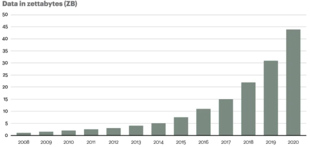
In 1944 Fremont Rider estimated that American university libraries were doubling in size every sixteen years [1]. Rider said: “Yale Library in 2040 will have approximately 200,000,000 volumes, which will occupy over 6,000 miles of shelves”. The following years were characterised by rapid techno-logical advancements and stored information slowly moved from books and paper to digital devices. In 1996, R.J.T. Morris and B.J. Truskowski showed how cheaply data could be digitally stored [2]. In the following years (1997-2000), technology advanced even faster during the Dot-Com Bubble. This lead to the spread of the internet, the diffusion of cheaper hard drives and the availability of more processing power making data storage and process-ing even easier. In 2010 the Economist published an article titled "The Data Deluge" showing how the amount of data collected was exponentially increas-ing. According to the article, mankind created 150 exabytes (1017 bytes) of data in 2005 and 1200 in 2010 and some estimates say that, in 2010, 90% of the world data was generated during the last year. Figure 1.1 shows the expected amount of data generated in the world by year.
“Big Data” is the term commonly used to refer to the large and complex datasets available. Big Data is commonly characterised by three character-istics reffered as the three Vs of Big Data [3]: Volume, Variety and Velocity. Volume refers to the large amount of data; Variety to the different formats of the data and the different sources of information; Velocity refers to the speed with which data is generated and collected.
Figure 1.1: The expected amount of data generated in the world according to Oracle. (1 zettabyte =1021 bytes).
incredible amount of data is continually generated. In recent years, thanks to the availability of cheaper sensors and measurement tools, the use of Big Data expanded to several sectors such as: health care, manufacturing, retail and security. This thesis focuses on applications in the semiconductor manu-facturing industry, a field that is starting to rely heavily on data to improve production.
1.2
Semiconductor Manufacturing
Semiconductor manufacturing is one of the largest industries in the world, employing almost 250,000 people in the USA alone [4]. It posted sales glob-ally totalling 335.2 billion dollars in 2015 [5] and sales are expected to con-tinue to grow in the future as shown in Figure 1.2. Some big companies in the area, and their revenue in 2012, are reported in Table 1.1. Market demand and fierce competition has driven restless innovation in the sector. As a consequence, research and development (R&D) has always been at the forefront of semiconductor manufacturing.
Since the invention of integrated circuits in 1960, the number of transistors on an integrated circuit has doubled roughly every 2 years as predicted by Moore’s law [6]. To maintain the pace of development set by Moore’s law, production processes in semiconductor manufacturing are becoming more and more complex, consisting of several hundred processing steps. Better device performance and greater production throughput are achieved by
re-Figure 1.2: The global semiconductor market from 2015 through 2025. re-Figure and data from SEMI (http://www.semi.org)
Company Name 2012 Revenue in Million of Dollars
Intel 47,543
Samsung Electronics 30,474
Qualcomm 12,976
Table 1.1: Top three semiconductor manufacturing companies and their rev-enue in 2012.
ducing circuit critical dimensions, improving processor architecture, increas-ing wafer size and by improvincreas-ing product consistency and uniformity.
Every two years, the International Technology Roadmap for Semiconductors (ITRS) indicates research areas where more innovation is required and pro-vides guidelines for the use of research funds. The 2007 ITRS roadmap [7] defines the wafer design parameters over an 8-year period. In order to meet the industry historical 30% cost-per-function reduction, and 50% cycle time improvement in manufacturing per decade, the wafer diameter is required to increase from 300 to 450mm while the critical dimensions are required to decrease from 80 to 22nm.
In order to mantain market share and remain competitive, it is essential to keep production costs low. In the past cost reductions were achieved via yield improvement. As yield improvements are more and more difficult to achieve, further improvement can be obtained by maximizing throughput of products with reduced setup and maintenance costs [8]. This has led to the adoption of statistical process control (SPC) techniques to monitor process faults and anomalies, with its use in fabs expanding rapidly between the 1980’s and the 1990’s. However, as production processes have became more complex, traditional SPC is no longer adequate leading to an increasing number of false alarms and undetected anomalies. In a modern manufacturing plant, a chip costs, on average, $40 and a wafer contains roughly 450 chips. The cost of producing a faulty wafer is therefore of the order of $22,500.
In order to improve on SPC, the use of advanced process control (APC) spread. APC refers to a broad range of techniques and technologies employed to maximise the use of available information about materials and processes. APC analyses diagnostic data and desired targets, selects model and control strategies, estimates the feasibility of the desired targets and generates the necessary alarms for process faults. APC is usually deployed optionally and, in addition to basic SPC, and developed over a period of time with the aim of solving specific problems [8].
1.2.1
Wafer Processing
Semiconductor device fabrication is a complex process. The main steps in-volved are represented in Figure 1.3. Among these, plasma etching has been recognized as one of the operations which has a decisive influence on product quality and has been the focus of many studies [9].
Figure 1.3: Wafer processing steps. Figure from Lam Research (http:// www.lamresearch.com/products/products-overview).
1.2.2
Plasma Etching
In the late 1960s, plasma etching, a form of plasma processing used for in-tegrated circuit (IC) manufacturing, emerged as an alternative to acid bath chemical etching (wet etching, [9]). In contrast to chemical etching, plasma etching can be directed. An highly directional etching process is desirable to guarantee product quality and avoid problems such as short circuits [10]. Figure 1.4 shows the differences between plasma etching and chemical etch-ing; the former leads to a more precise and controlled etching and is able to shape the wafer surface as required.
Due to its physical structure plasma emits light and this light has been proven to be a reliable indicator of plasma chemistry. This can be collected non-intrusively during etching through the use of an Optical Emission Spectrom-eter [11]. The resulting Optical Emission Spectroscopy (OES) data allows real-time plasma monitoring and is a starting point for the application of APC to a plasma etching process [12]. Despite this, the application of APC to plasma etching processes remains challenging, due to the highly complex plasma physics and etching chemistry involved and the sensitivity of plasma to subtle process variations. In addition, OES data is generally character-ized by high dimension (typically >2000 variables) and highly redundant variables, making its use and analysis challenging.
The OES data is generally represented as a matrix X ∈ Rn×p where each
column is a time series containing the intensity at a particular wavelength over time. In the rest of the thesis, with an abuse of notation, the term
"wavelength" is often used to indicate the intensity at a given wavelength or one of the columns of X. This will not lead to confusion as the meaning of wavelength will be clear from the context. A more detailed description of the OES data will be presented in Chapter 2.
Figure 1.4: Difference between plasma (Anisotropy) and chemical (Isotropy) etching. Figure from Minh Anh Thi Nguyen.
1.3
High Dimensional Data and the Curse of
Dimensionality
High dimensional datasets are difficult to deal with on several counts. If the number of variables is larger than the number of measurements, each variable can be obtained as a linear combination of the others making uncovering the true relationship between the different variables difficult. This is a common scenario in semiconductor manufacturing as the number of measurements often corresponds to the number of processed wafers and that is generally much smaller than the number of measured variables. Furthermore, high di-mensional datasets are impacted by the so called "Curse of Didi-mensionality"
according to which distance measurements between samples become unreli-able. In addition, high dimensional datasets are difficult to interpret, which in turn makes extracting useful process insight challenging. From a com-putational perspective, the curse of dimensionality can mean an exponential growth in computational complexity with dimension, leading to computation time problems. Addressing computational bottlenecks and developing com-putationally efficient algorithms is therefore critical when working with high dimensional data.
For any practical application, the dimensionality of the OES data needs to be reduced. Traditionally engineering knowledge of the underlining process chemistry can be used to extract the most relevant wavelengths from the OES data [13]. This process is problematic as it is time consuming, biased by the engineer’s personal experience, and is limited to a particular process. Given changes in the process recipes or etching products, the effectiveness of the selected wavelengths can be reduced. As a consequence, more automated and unbiased techniques are required.
1.3.1
Dimensionality Reduction and Variable Selection
Highly dimensional datasets are not only present in semiconductor manu-facturing, but are common in many fields such as image processing [14] and genetics [15]. As a consequence, a lot of interdisciplinary research is involved in the area and several dimensionality reduction algorithms have been devel-oped.Dimensionality reduction algorithms are, in general, based on feature ex-traction. This is a well known machine learning problem that was originally investigated in the field of pattern recognition and image processing. Feature extraction summarises the data with basic components that seek to extract all the information that is required for a given task. Feature extraction tech-niques are now widely applied in several fields in different forms. Due to this variety, it is impossible to provide an accurate definition of feature extrac-tion. As Selfridge and Neisser [16] pointed out, feature extraction algorithms have to be designed individually to effectively tackle an unknown issue. Feature extraction is, in general, performed trough the use of data driven black-box algorithms. The extraction methodologies are then widely appli-cable but the obtained features loose their physical meaning. This problem can be avoided with the use of variable selection algorithms. Variable
se-lection is equivalent to feature extraction, but the extracted features are constrained to be a subset of the original variables. This allows interpretable APC procedures to be developed and enables engineers to rapidly understand the root causes of faults or process variations.
Variable selection algorithms can be divided into three categories: supervised variable selection, semi-supervised and unsupervised variable selection [17]. In supervised variables selection the choice of the variables is guided by a target variable and the goodness of the selection is evaluated based on the obtained prediction performance. In the semi-supervised and unsupervised variable selection, instead, variables are selected in order to summarise the majority of the data looking for the right balance between number of selected variables and information loss, that, according to the application, can be measured with different metrics. The difference between an unsupervised and a semi-supervised analysis is that, in the first case, no information about the data is available while in the second case the data is known to contain only samples of a given category as. for example, only normal behaving wafers.
1.4
Aims and Scope of the Thesis
This thesis aims to develop techniques that enable OES measurements to be used effectively in a semiconductor manufacturing production process. A full industrial case study is discussed from the collection of the OES data to its application for virtual metrology and anomaly detection. Particular focus is on the development of supervised and unsupervised variable selection techniques, a fundamental step for any practical application of the OES data. In the unsupervised context, the aim of these algorithms is the definition of a set of variables that are able to summarise the full original data X. In a supervised context the aim is to identify the smallest set of variables from X
that allows an external signal yto be reconstructed.
1.5
Contributions
This thesis claims the following original contributions:
1. A spectral alignment procedure which aligns OES measurements from multiple sensors through a retrospective calibration process that cor-rects for inter-spectrometer variation in the mapping from wavelengths to spectrometer channels based on the Particle Swarm Optimization
algorithm [18]. The calibration process involves estimation of a cor-rection function using Particle Swarm Optimization. PSO is needed because the cost function associated with the problem is non convex and multi-modal.
2. An investigation of the performance of the lasso algorithm with differ-ent types of cross-validation and the developmdiffer-ent of improved versions of lasso denoted as: High Frequency, High Mean, Monte Carlo High Frequency and Monte Carlo High Mean. The proposed methods stabi-lize the set of variables selected by lasso and have equivalent or lower prediction error to competing approaches.
3. A detailed presentation of the Forward Selection Component Analysis (FSCA) algorithm and the development an analysis of computationally efficient algorithm implementations [19].
4. A number of new variants of the FSCA algorithm that incorporate a refinement step to improve performance are proposed.
5. The development of nonlinear extensions of the Forward Selection Com-ponent Analysis and Forward Selection Variables algorithms. The newly proposed methods have roughly the same computational com-plexity as their linear counterparts but result in much better perfor-mance [20].
6. An unsupervised variables selection algorithm based on deep neural networks is proposed. This is competitive with and sometimes bet-ter than the linear-in-the-paramebet-ter nonlinear extension of Forward Selection Component Analysis (FSCA), but at the expense of higher computational complexity.
7. The effect of dimensionality reduction on anomaly detection is inves-tigated. Forward Selection Independent Variables is proposed as a new unsupervised variables selection algorithm specifically designed for anomaly detection [21].
Other contributions in the thesis includes:
1. A review of the methodologies used to define a solution of the lasso estimator.
2. A review of unsupervised variables selection algorithms and a definition of data decomposition and reconstruction in an unsupervised variables selection context.
3. Extreme Learning Machines (ELM) neural networks are for the first time applied to a virtual metrology problem. Methodologies to auto-matically select the number of hidden nodes and weights initialization of ELMs are proposed [22].
4. A review of unsupervised anomaly detection algorithms for anomaly detection with OES data.
5. The Unsupervised Random Forest algorithm is for the first time applied for anomaly detection with OES resulting in good performance even for high dimensional datasets [23].
6. The Isolation Forest algorithm is for the first time applied to the OES data for anomaly detection and diagnosis using a newly proposed di-agnosis procedure.
7. The Similarity Ratio algorithm for anomaly detection with OES time series is generalized and extended to multivariate anomaly detection. 8. A first application of Forward Selection Independent Variable Selection
and One Class Support Vector Machine algorithms to OES time series data based anomaly detection [21].
1.5.1
List of Publications
• Puggini Luca, John Doyle and Seán McLoone. "Towards multi-sensor spectral alignment through post measurement calibration correction."
Irish Signals and Systems Conference 2014 and 2014 China-Ireland International Conference on Information and Communications Tech-nologies (ISSC 2014/CIICT 2014). 25th IET. IET, 2013.
• Puggini Luca, John Doyle and Seán McLoone. "Fault Detection us-ing Random Forest Similarity Distance." IFAC-PapersOnLine 48.21 (2015): 583-588.
• Puggini Luca and Seán McLoone. "Extreme learning machines for virtual metrology and etch rate prediction."Signals and Systems Con-ference (ISSC), 2015 26th Irish. IEEE, 2015.
• Puggini Luca and Seán McLoone. "Feature Selection for Anomaly De-tection Using Optical Emission Spectroscopy." 4th IFAC International Conference on Intelligent Control and Automation Sciences (ICONS 2016).
• Puggini Luca and Seán McLoone. "Nonlinear Forward Selection Com-ponent Analysis for Optical Emission Spectroscopy Wavelength Selec-tion."Signals and Systems Conference (ISSC), 2016 27th Irish. IEEE, 2015.
• Puggini Luca and Seán McLoone. "Forward Selection Component Analysis: Algorithms and Applications." under review at IEEE trans-actions on pattern analysis and machine intelligence.
1.6
Thesis Structure
The reminder of the thesis is organised as follows:
Chapter 2 begins with an introduction to plasma, plasma etching and Optical Emission Spectroscopy (OES) plasma measurements. In the chapter a formal mathematical framework to describe OES time series is introduced, the PSI and J2M datasets are introduced as industrial case studies and the multi-chambers matching problem is discussed. Finally, a novel spectral alignment procedure that corrects for wavelength misalignment between spectrometers is developed.
Chapter 3 focuses on supervised variables selection and the lasso estimator. The stability of the lasso is investigated and algorithms to detect a stable set of variables are proposed. Evaluations are performed and results presented for a series of benchmark datasets.
Chapter 4 presents novel research on linear unsupervised variables selection. It starts with a review of the most popular unsupervised variables selection algorithms and then provides a detailed description of the Forward Selection Component Analysis algorithm. This is extended though the development of an alternative implementation and the introduction of different refine-ment steps. The extended methodology is compared with the basic ones and similar algorithms taken from the literature using a series of simulated and real-world case studies.
Chapter 5 extends the linear unsupervised variables selection algorithms de-scribed in the previous chapter through the introduction of multivariate non-linear models. The chapter starts with a description of neural networks and the Extreme Learning Machines algorithm. It is shown how the method can be improved and used with minimal user intervention. Extreme Learning
Machines Neural Networks are then used with other linear-in-the-parameters nonlinear multivariate algorithms for nonlinear unsupervised variables tion. The use of a multilayer neural network for unsupervised variables selec-tion is also investigated. Comparison is performed between the new nonlinear algorithms and linear principal component analysis based unsupervised vari-able selection and linear dimensionality reduction.
Chapter 6 focuses on anomaly detection with application to OES data. The chapter starts with a survey of unsupervised anomaly detection algorithms that work well with highly dimensional datasets. In the second part of the chapter the effect of dimensionality reduction on anomaly detection is in-vestigated. Here, an unsupervised variables selection algorithm specifically designed for anomaly detection is proposed. In the last part of the chapter, the proposed techniques are investigated for anomaly detection using an OES time series dataset as a case study.
Chapter 7 provides a concluding summary of the work done and of the pro-posed methodologies as well as possibilities for future research.
1.7
Notation
The mathematical notation and conventions used in the thesis are introduced here. This notation holds in most circumstances with a few exceptions where changes are appropriately introduced.
• Matrices are indicated with a bold capital letter as: X,Y,Z,W,Λ, . . .. In general Xdenotes an input dataset and Zthe matrix obtained with a subset of the columns of X.
• In general, when referring to a dataset X, n is the number of samples and p is the number of variables. Each column of X corresponds to a variable and each row to a sample. It follows thatX∈Rn×p. k is often
used to indicate the number of features extracted from X and if Z is the matrix composed of those features it follows that Z∈Rn×k. • Column vectors containing the n measurements for a given variable
are indicated with a bold lower case letter as: x,y,z,· · · ∈ Rn. The
elements of each vector are indicated with the same letter with an index determining the position in the vector e.g. x= (x1, x2, . . . , xn).
given observation is represented as a bold lower case letter with an arrow on the top: ~x, ~y, ~z,· · · ∈Rp
• Matrices can then be obtained by horizontally stacking column vectors or by vertically stacking row vectors, that is:
X= (x1, . . . ,xp) = ~x1 ~x2 · · · ~ xn = x1,1 x1,2 . . . x1,p x2,1 x2,2 . . . x2,p · · · xn,1 xn,2 . . . xn,p ∈Rn×p
• Given a probability distribution D (for example N(0,1)), p random variables following the distribution are indicated as x1, . . . , xp ∼ D.
There is often an implicit transformation between the random variable
xi and the vector containing the sampled values xi. For simplicity, in
some cases, we will write x ∼ D with x ∈ Rn indicating the vector
Optical Emission Spectroscopy:
Collection and Representation
2.1
Introduction
The focus of this thesis is on the development of computational intelligence techniques for Optical Emission Spectroscopy (OES) data analysis. Dealing with OES data is, in general, challenging due to its size and complexity. Before performing any analysis on the data or using it for any industrial ap-plication it is important to have a good understanding of its characteristics and how it is collected. With this in mind, the aim of this chapter is to pro-vide a detailed description of OES data, focusing in particular on problems related to data collection and data representation. In this sense, a mathe-matical formalism to describe OES time series data is reported and a data format that facilitates the analysis of differences between wafers in a time interval during the production is proposed. In an industrial environment, OES data is commonly collected with different sensors. Nonlinearities in the response of OES sensors and errors in their calibration lead to discrepancies in observed wavelength detector responses, with the result that wavelengths are misaligned when comparing data from different spectrometers. As the quality of the available measurements strongly influences the performance of any analytical method the multi-sensor matching problem is investigated and a procedure based on Particle Swarm Optimization (PSO, [24]) developed to retrospectively align OES data from multiple sensors.
The chapter is divided into three main sections. Section 2.2 contains a basic introduction to plasma, a description of the plasma etching chamber and of the optical emission spectrometer from which the OES measurements are
col-lected. In section 2.3 a mathematical description of the OES data is provided and some of the industrial case study datasets that will be used throughout the thesis are introduced. The Λ and W data formats are also introduced. They are particularly important for Chapter 6 where anomaly detection with OES data is investigated. Finally, section 2.5 describes the multi-sensor spec-tral alignment problem and the proposed retrospective alignment algorithm.
2.2
Plasma Etching and Optical Emission
Spec-troscopy
In this section the scientific principles of optical emissions from plasma and measurement techniques are introduced. In particular, a description of some basic plasma, plasma etching and optical emission spectrometer concepts are provided.
2.2.1
Plasma
Plasma is a form of matter in which many of the electrons wander around freely among the nuclei of the atoms. Normally the electrons stay with the same atomic nucleus but in a plasma, a significant number of electrons have such high energy levels that no nucleus can hold them. In a plasma the generation of the electrons and ions results from a series of collisions, which are referred to as electron impact ionization, excitation, relaxation and recombination [25].
Definition 2.2.1 (Ionization with electron). When an incoming ion or elec-tron with enough energy collides with an atom, the outermost elecelec-tron of this atom can absorb energy to break the electric potential barrier that originally bound it to the atom. This results in a free moving electron and an equally charged ion. Defining A as the atom, the ionization of A can be expressed as:
e−+A→2e−+A+ (2.1)
Definition 2.2.2 (Excitation). Excitation refers to the process of a plasma atom being activated to a higher energy level when colliding with a free moving electron, but where the absorbed energy is not enough, to break the electric potential barrier to form a free moving electron. The process can be summarised as:
where A∗ represents the excited atom.
In other words excitation results in the alteration of the state of an atom, ordinarily, from the condition of lowest energy (ground state) to one of higher energy (excited state). Excited atoms return to their original state by releas-ing energy through a phenomena called relaxation.
Definition 2.2.3 (Relaxation). Relaxation refers to the process of the elec-tron in an elecelec-tronically excited atom transiting from a higher energy level to a lower energy level with excess energy released in the form of a photon.
A∗ →A+E (photon) (2.3) A photon is a discrete packet of energy associated with electromagnetic ra-diation (light). The wavelength of the emitted light corresponds to exactly the energy difference between the two energy levels with
E = hc
λ (2.4)
where λ denotes the wavelength of the photon, c denotes the speed of light andhis Planck’s constant. Thus, an atom emits light at only certain discrete wavelengths. Each atomic and molecular species has its own unique spectral signature, hence by analysing the optical emission from a plasma its compo-sition can be determined. This phenomenon leads to the characteristic light emission of a plasma.
Definition 2.2.4 (Recombination). Recombination refers to the process of an electron being combined with an ion to form a neutral atom. However, a third body is required to take part in the process to allow the recombination to satisfy the conservation of energy and momentum requirements [25]. The recombination process can be expressed as:
e−+A++A→A+A (2.5)
2.2.2
Plasma Etching
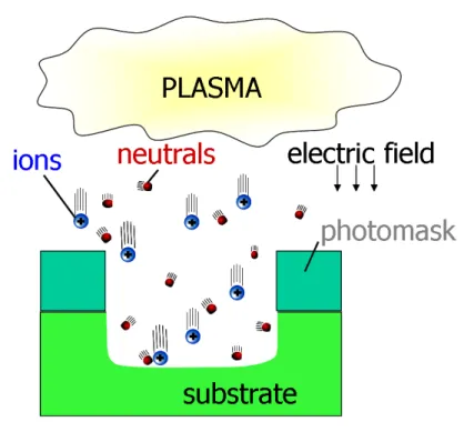
In semiconductor manufacturing, plasma is, in general, generated though the application of microwave energy to a gas. Radio Frequency (RF) directs the ions toward the wafer surface where they interact both chemically and phys-ically with the silicon wafer, etching away the exposed surface [26]. Figure 2.1 provides a graphical representation of the plasma etching process.
Figure 2.1: Plasma etching process. The ions bombard the exposed surface. Figure from https://www.scorec.rpi.edu.
2.2.2.1 Electron Cyclotron Resonance Plasma Etcher
Plasma etching takes place in a plasma etcher. In this section an Electron Cyclotron Resonance plasma etcher is considered.
Definition 2.2.5 (Electron Cyclotron Resonance). Electron Cyclotron Res-onance (ECR) refers to the phenomenon according to which a electron in a static and uniform magnetic field will move in a circle due to the Lorentz force.
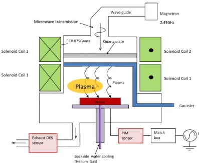
The ECR plasma etcher makes use of microwave energy and a strong mag-netic field to produce a low pressure and high density plasma and provides the necessities for achieving plasma etching [27]. The main components of an ECR etcher include a magnetic field generation system, a microwave os-cillator, a gas supply system, a Radio Frequency (RF) generator and an etch chamber, as illustrated in Figure 2.2. A microwave power supply generates microwave which are oscillated by a magnetron, transmitted along a waveg-uide and injected into a quartz plate. The microwaves produce a dynamic electric field, which is perpendicular to the static magnetic field, which is generated as a DC current flowing through the solenoid coils. The interac-tion of these two fields generates a Lorentz Force, which causes the electrons to spiral in a helical motion. In this way, the microwaves transfer the en-ergy to free electrons which in turn accelerate and collide with the atoms or molecules in the gas and produce ionization. The low gas pressure, which helps to reduce electron impact recombinations, is achieved by controlling the flow rates of the gases supplied to the chamber. A separate RF bias is applied to the wafer electrode to independently control ion energy at the wafer surface. The wafer temperature, which is an important factor influenc-ing the uniformity of etch across the wafer surface, is reduced with the use of helium. An important feature of the ECR etcher is that ion energies can be controlled separately by the RF supply, allowing much greater control of etch rate. An OES (Optical Emission Spectroscopy) sensor and a PIM (Plasma impedance monitor) sensor are also shown in the figure. These can be used to monitor the optical and electrical characteristics of the plasma, respectively. In this thesis, we are concerned exclusively with analysing OES data.
2.2.3
Optical Emission Spectrometer
Analysis of plasma emission spectra can be used to estimate the instanta-neous composition of a plasma over time. An Optical Emission Spectrometer is an optical device used to detect the optical emissions of plasma species,
Gas inlet Quartz plate
ECR 875Gauss
RF PIM
sensor Match box
Solenoid Coil 2 Solenoid Coil 2
Solenoid Coil 1 Solenoid Coil 1 Microwave transmission Wave-guide Magnetron 2.45GHz Wafer
Backside wafer cooling (Helium Gas)
Plasma Plasma
Exhaust OES sensor
Figure 2.2: Illustration of the basic features of a plasma etching chamber.
providing direct information on plasma chemistry [11]. In Optical Emission Spectroscopy (OES), visible light is collected and redirected onto a Charged Coupled Device (CCD) detector with different wavelengths dispersed to dif-ferent CCD [28]. The key component of a typical Optical Emission Spec-trometer is the CCD detector. CCDs are a type of quantum detectors, which are used to measure the flux of photons. CCDs have been widely employed in modern optical detection devices for their fast response time and sensitivity to small photon fluxes.
2.2.3.1 Data Collection During Plasma Etch Processing
In a production process wafers are usually grouped in lots, with wafers in a lot arranged in slots on a cassette. Wafers in a lot are processed sequentially (according to slot number) undergoing several etching steps. Lots are are also processed sequentially through etch chambers, interspersed with clean-ing and maintenance operations. Cleanclean-ing cycles are typically done between each lot to remove the by-products of plasma etching that build up on the chamber walls, and are detrimental to etching performance. This leads to a chamber seasoning effect during the first few wafers processed following each cleaning cycle, and consequently slot dependent differences in processed wafers. A consequence of this is shown later in Figure 2.11.
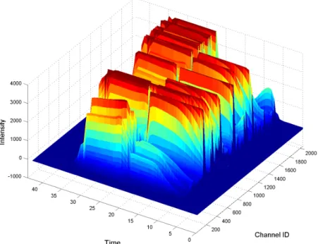
In this work the considered OES datasets are collected using Ocean Optics USB2000 spectrometers with CCD detectors consisting of a variable number of channels each one recording a single wavelength. Wavelength intensity measurements are taken without interruption with a fixed sampling rate dur-ing processdur-ing of wafers. This results in chronologically ordered values for a set of wafers. Figure 2.3 shows the graphical representation of the OES measurements for an example wafer. In this example wavelength intensity was measured during 40 seconds of plasma etching, at a sampling rate of 1 second for p= 2000channels.
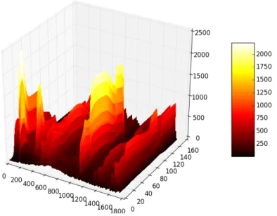
Figure 2.3: Plasma etch OES data for a single wafer (Xk), recorded over two
etching steps. The units on the time axis are in seconds.
2.3
Mathematical Representation of OES Data
In the previous section the physical concepts behind plasma and the tools that are used to collect the OES measurements are described. In a produc-tion environment the OES measurements are collected continually at a fixed sampling interval while the wafers are processed resulting in OES time series data. In this section the OES time series data is described and some datasets that will be used throughout the thesis are introduced.2.3.1
Wafer Measurements
As noted in [12] plasma etch processing OES data is naturally organized in three dimensions: Wafer; Time; and Wavelength. With this in mind it is reasonable to represent a generic element of the OES data as:
xwk
i (t) (2.6)
This represents the intensity of theithwavelength at timetfor thek-th wafer. In this chapter K represents the total number of wafers and pthe number of wavelengths. It is assumed that the whole production ends after T samples and that during production τ equally spaced measurements are taken for each wafer. While this is not entirely true, it is a good approximation of the reality and it is required in order to define a formal structure for analysis. Given these assumptions the OES spectrum for a single wafer wk can be
mathematically represented as a matrix Xk ∈Rτ×p, where τ is the number
of time samples andpis the number of wavelengths measured during etching, that is: Xk = xwk 1 (t(k−1)τ+1) xw2k(t(k−1)τ+1) · · · xwpk(t(k−1)τ+1) xwk 1 (t(k−1)τ+2) xw2k(t(k−1)τ+2) · · · xwpk(t(k−1)τ+2) · · · xwk 1 (t(k−1)τ+τ) xw2k(t(k−1)τ+τ) · · · xwpk(t(k−1)τ+τ) ∈Rτ×p (2.7) In some cases, in order to simplify the notation, xwk
i (t(k−1)τ+j) is denoted as
xwk
i (tj). OES time series datasets thus st of as a set of matrices where each
one contains the spectrum for a given wafer:
S =Xj ∈Rτ×p : j = 1, . . . , K (2.8)
Under the assumption that measurements are recorded at τ time points for each wafer, the data in the set S can then be represented as a three dimen-sional matrix.
X∈RK×p×τ (2.9)
where K corresponds to the number of wafers, p to the number of wave-lenghts and τ is the number of samples recorded for each wafer. Similar representations are reported in [29].
For practical applications this three dimensional matrix can be reshaped in a two dimensional matrix in three different ways:
• Aggregated by Wafer. The data is stored in a matrix W ∈RK×pτ • Aggregated by Wafer Processing Time. The data is stored in a matrix
F∈Rτ×pK
A deeper description and an analysis of the data aggregated in the three matrices Λ,W and Fwill follow in the next sections.
2.3.2
OES by Time Point
The data can be aggregated in a Λ∈Rτ K×p matrix. Here each row contains
a sample instant and each column corresponds to a wavelength. This format corresponds to the way the data is usually collected during production as the samples (rows) are chronologically ordered. Λ can be formed by vertically stacking the set of matrices S, i.e.
Λ= X1 X2 · · · XK ∈RKτ×p (2.10) More specifically, Λ= xw1 1 (t1) xw21(t1) · · · xwp1(t1) xw1 1 (t2) xw21(t2) · · · xwp1(t2) · · · · xw1 1 (tτ) xw21(tτ) · · · xwp1(tτ) xw2 1 (tτ+1) xw22(tτ+1) · · · xwp2(tτ+1) · · · · xwK 1 (T) x wK 2 (T) · · · xwpK(T) (2.11) or equivalently Λ= xw1 1 (t1) xw21(t1) · · · xwp1(t1) xw1 1 (t2) xw21(t2) · · · xwp1(t2) · · · · xw1 1 (tτ) xw21(tτ) · · · xwp1(tτ) xw2 1 (t1) xw22(t1) · · · xwp2(t1) · · · · xwK 1 (tτ) xw2K(tτ) · · · xwpK(tτ) (2.12)
Each column of the Λ matrix is a time series representing a wavelength over
K wafers. Two sample columns of the Λ matrix are plotted in Figure 2.4. The figure shows the periodic repetition of values that corresponds to the
different wafers. According to [12] this data format is particularly useful when performing wavelength selection. This simply follows from the fact that each column is a different wavelength. An example of this will be shown in Chapter 6 as an application of anomaly detection with OES data.
0 200 400 600 800 1000
t
0 500 1000 1500 2000 2500Intensity
0 200 400 600 800 1000t
0 10 20 30 40 50 60 70Intensity
Figure 2.4: Two sample columns of the Λ matrix.
2.3.3
OES by Wafer
Alternatively the wafers in S can be aggregated in the wafer format as a matrix W. In the W matrix each row corresponds to a wafer and each column contains the measurements of a given wavelength at a given time. W
is obtained by transforming the elements of S into row vectors and stacking them vertically. Mathematically given a sample element of S:
Xk = xwk 1 (t1) xw2k(t1) · · · xwpk(t1) xwk 1 (t2) xw2k(t2) · · · xwpk(t2) · · · · xwk 1 (tτ) xw2k(tτ) · · · xwpk(tτ) ∈Rτ×p (2.13)
it is reshaped as a row vector
˜
Xk = (xw1k(t1), . . . , xpwk(tτ))∈R1×τ p (2.14)
and theWrepresentation is obtained by combining all the reshaped matrices in S to give:
W= ˜ X1 · · · ˜ XK ∈RK ×τ p (2.15) or equivalently W= (W1, . . . ,Wp)∈RK×τ p (2.16) where Wi = xw1 i (t1) xwi1(t2) · · · xwi 1(tτ) xw2 i (t1) xwi2(t2) · · · xwi 2(tτ) · · · · xwK i (t1) xwiK(t2) · · · xwiK(tτ) ∈RK×τ i= 1, . . . , p (2.17)
When the data is stored in the W format each sample (row) represents a single wafer. This representation of the OES data is convenient for comparing the characteristics of different wafers. It was, for example, used in [30] for an anomaly detection task. A challenge with this representation is that the number of columns (or variables) increases dramatically.
2.3.3.1 Time Window
In some circumstances it is important to analyse the difference between wafers at a given time interval during the etching process. This is for ex-ample used in Chapter 6 to understand when during the production a fault occurred and can be used to perform on-line analysis during the etching pro-cess. With this in mind an alternative data representation based on the W
format is proposed as follows.
Taking into account the fact that each column of Wis associated with a dif-ferent sample instant/wavelength combination, the variables can be grouped in matrices according to their t value. Sorting the columns of the W matrix (Equation 6.57) in chronological order it is possible to write:
WT = (Wt1,Wt2, . . . ,Wτ) (2.18) where Wti = xw1 1 (ti) xw21(ti) · · · xwp1(ti) xw2 1 (ti) xw22(ti) · · · xwp2(ti) · · · xwK 1 (ti) xw2K(ti) · · · xwpK(ti) ∈RK×p i= 1, . . . , τ (2.19)
The matrix
Wtj
ti = (W
ti,Wti+1, . . . ,Wtj)∈
RK×(tj−ti)p (2.20)
contains the information required to analyse the process between time ti
and tj. If the time interval [ti, tj] is sufficiently small the dimension W tj
ti
will be small enough to avoid the need for further dimensionality reduction. Increasing the value of ti and tj it is possible to analyse the full process
using the full information available for a given time interval and to use only
p(tj−ti)variables each time. In Chapter 6 this approach is used for anomaly
detection and to understand when during a wafer processing the anomaly occurred.
2.3.4
OES by Time
The third and final way to aggregate the data is to stack the matrices in S
horizontally, that is
F= (X1, . . . ,XK)∈Rτ×pK (2.21)
where Xk, as defined in equation 2.7, contains the OES measurements for
the kth wafer. The F matrix can be used to analyse the process in time. For example a PCA analysis of FT can detect redundancy along the time
dimension of the data, suggesting that it is sufficient to analyse the process at only few instants (sampling points). The F matrix is not used for any application in this thesis and it is reported only for completeness.
2.4
Industrial Case Studies
In this section two industrial datasets are introduced. These will be used as case studies throughout the thesis.
2.4.1
PSI Time Series
The first production dataset referred to as the PSI Time Series (PSI) dataset. This dataset contains all OES measurements collected from a single plasma etch chamber over several months.
Dataset 2.4.1 (PSI Time Series). The PSI dataset contains the measure-ments ofp= 1747wavelengths related to the production ofK = 1006wafers divided in 83 lots (with up to 25 wafers per lot). All the wafers were pro-cessed according to the same recipe and propro-cessed in 7 steps for 3 different
products. The number of samples recorded for each wafer varied in the range τ ∈[184,192]. Following an initial preprocessing step to remove irrel-evant data the number of time samples per wafer was reduced to τ = 165
with a sampling period of 0.5 seconds. The reasons for and the method used to achieve this reduction are described later in the thesis (Observation 2.4.1). After the preprocessing step the reference values for this datasets are
K = 1006, τ = 165 and p = 1747. A summary of the data is reported in
Table 2.1 and Figure 2.5 shows the number of wafers per lot. The figure shows that most lots contain 12 or 13 wafers. This follows from the fact that a lot in general contains only odd or even slot numbers. A few lots contain less than 5 wafers. These slots were probably occupied by particular wafers that were used for monitoring and cleaning. These wafers were removed as they are not relevant for the considered analysis.
F eature T otal N umber
Wavelengths 1747
Wafers 1006
Time points for each wafer 165
Total time points 190406
Lots 83
Slots 25
Recipes 1
Steps 7
Table 2.1: Summary of the PSI dataset (Dataset 2.4.1)
Figure 2.6 shows the variation in OES spectrum wavelength values during wafer processing. In the figure each coloured line corresponds to a row of the matrix Xk. To aid visualisation only 5 selected rows of Xk are plotted.
The mean: ¯ S= 1 K K X k=1 Xk ∈Rτ×p (2.22)
and the standard deviation:
Std(S) = 1 K −1 K X k=1 (Xk−S¯)2 (2.23)
obtained for the PSI data (Dataset 2.4.1) after some data cleaning steps are shown in Figures 2.7 and 2.8.
0 2 4 6 8 10 12 14
Number of Slot per Lot
0 5 10 15 20 25 30 35 40 45
Count
Figure 2.5: Number of slots in each lot for Dataset 2.4.1.
Observation 2.4.1. The hypothesis that each wafer is processed during the same amount of time τ is required in order to create a one to one relationship between wafers at a given time:
xwv
i (tj)−→xwiu(tj) (2.24)
i. e.
xwv
i (tτ(v−1)+j)−→xiwu(tτ(u−1)+j) (2.25)
In a real-time production scenario this is often not exactly true and the data may require a preliminary cleaning step. In the considered data, for example, during the processing of some wafers, the machine started to record wave-length values before wafer processing had actually started. As a consequence the time point measurements for some wafers are preceded by some zeros for each wavelength i.e.
∀j xwk
j (ti) = 0 f or i= 0, . . . , zwk (2.26)
where zwk is defined as:
zwk =minz: xwk
j (tz+1)>0 (2.27)
In order to align the start of etching for each wafer these initial zeros are removed, i.e.:
xwk
0
200
400
600
800
1000 1200 1400 1600 1800
Wavelengths
0
500
1000
1500
2000
Intensity
Figure 2.6: An illustration of the variation in OES spectrum wavelength intensities over time for a given wafer. Each line spectrum represents a different time instant (sample).
Figure 2.7: The 3-dimensional representation of the mean of the PSI dataset (Dataset 2.4.1) as defined in equation 2.22 for t <150.
Figure 2.8: The 3-dimensional representation of the standard deviation of the PSI dataset (Dataset 2.4.1) as defined in equation 2.23 for t <150.
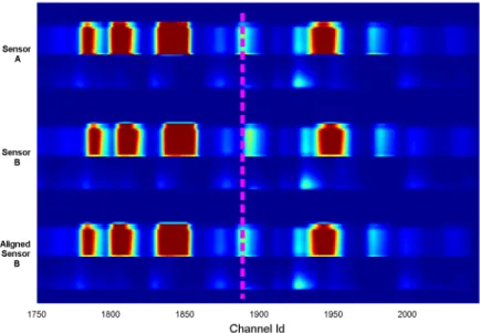
Figure 2.9 shows the traces for a given wavelength of several wafers before and after alignment. In the first plot the wafer represented by a red line is slightly shifted with respect to the others while all the wafers are aligned in the second plot. Several problems may arise if the data is not properly aligned. In an anomaly detection context for example the misaligned wafers will be wrongly labelled as an anomaly. A similar problem is investigated in Chapter 6.
Henceforth, unless otherwise stated wafer {Xk}k=1,...,K will be assumed to be
aligned and the same length (τ samples).
0
50
100
150
200
0
10
20
30
40
50
60
0
20
40
60
80
100 120 140 160 180
t
0
10
20
30
40
50
60
Figure 2.9: A given wavelength for 10 wafers before and after alignment.
2.4.1.1 PCA Analysis of the PSI Data
In order to better understand the structure of the PSI dataset a PCA analysis of the data presented in the W and Λ formats is performed.
W format PCA: TheWmatrix is scaled to unit variance and a PCA de-composition is performed. Due to the large size of the data and for computa-tional efficiency an approximation of PCA is obtained with the Incremental PCA algorithm [31]. The percentage of explained variance is plotted as a function of the number of components in Figure 2.10. The figure shows that
the percentage of explained variance grows quickly with the first20-30 prin-cipal components getting close to the70%. The following components do not contribute much in terms of explained variance. This reflects the redundancy of the data that can be summarised by only 30 components. The remaining components are associated with variations that are not representative of the majority of the data and are likely to be capturing the noise in the data. Figure 2.11 shows the projection of the Wmatrix onto its first five principal components. In the figure the samples are coloured according to their slot number. Particularly interesting is the projection onto the first principal component. In this case the samples on the left are coloured blue. These correspond to the samples with the lowest slot number. Gradually the colour of the samples changes from blue to red as we move from left to right with red corresponding to samples with the largest slot number. This suggests that theW format is particularly useful for detecting inner wafer variations. Indeed, in Chapter 6 good anomaly detection performance is obtained using datasets derived from the W format of the data.
0 20 40 60 80 100
PCs
60 65 70 75 80E
V
Figure 2.10: The percentage of explained variance by the first 100 P Cs of the Wmatrix for Dataset 2.4.1. The matrix was scaled in order to have unit variance.
Λ format PCA: The Λ matrix is scaled to unit variance and a PCA de-composition is performed. Figure 2.13 shows the percentage of explained variance as a function of the number of principal components. Seven
compo--1000-800-600 -400 -2000200 400
X
PC A 1 600 400 2000 200 400X
PC A 2 400 2000 200 400X
PC A 3 400 300 200 1000 100 200 300X
PC A 4 1000 800 600 400 200 0 200 400X
PCA 1 600 400 2000 200 400X
PC A 5 600 400 200 0 200 400X
PCA 2 400 200 0 200 400X
PCA 3 400 300 200 100 0 100 200 300X
PCA 4 600 400 200 0 200 400X
PCA 5Figure 2.11: Dataset 2.4.1: The scores obtained projecting the W matrix on the subspace generated by its first 5 P Cs. The data was scaled in order to have unit variance and the samples are coloured according to their slot number. -300 -200 -1000 100 200
X
PC A 6 400 2000 200 400X
PC A 7 500 400 300 200 1000 100 200X
PC A 8 400 300 200 1000 100 200 300X
PC A 9 300 200 100 0 100 200X
PCA 6 300 200 1000 100 200 300X
PC A 10 400 200 0 200 400X
PCA 7 500 400 300 200 100 0 100 200X
PCA 8 400 300 200 100 0 100 200 300X
PCA 9 300 200 100 0 100 200 300X
PCA 10Figure 2.12: Dataset 2.4.1: The scores obtained by projecting theWmatrix on the subspace generated by P Cs 6 to 10. The data was scaled in order to have unit variance and the samples are coloured according to theirs slot number.
nents explain more than 99% of the total variance. This is a consequence of the high level of redundancy in the data. In this data format each column is a wavelength. These are very correlated for physical reasons as they are all measurements of light emitted from plasma as described in section 2.2. Also the rows are highly correlated as they contain the time points that repeat almost periodically for each wafer afterτ samples (this was previously shown in Figure 2.4). Figures 2.14 and 2.15 show the projection of the rows of Λ
corresponding to two wafers from a randomly selected lot (one from slot 1 and one from slot 25) respectively onto the PCA subspace. It is interesting to observe that the measurements corresponding to the two wafers behave similarly in the subspace defined by the first 3 P Cs and start to behave differently onto the subspace generates by later P Cs. This is a consequence of the fact that the two wafers have a similar main trend given by the peri-odical repetition of values characterising each wafer and some higher order differences probably related to the seasoning effect.
0 20 40 60 80 100
PCs
97.0 97.5 98.0 98.5 99.0 99.5 100.0E
V
Figure 2.13: The percentage of explained variance by the first 100 P Cs of the Λ matrix for Dataset 2.4.1. The matrix was scaled in order to have unit variance.
2.4.2
J2M Dataset
J2M is the second semiconductor manufacturing dataset introduced in this section. It was obtained from an OES time series represented in theWformat through the use of summary statistics as defined in the next paragraph.
-60 -40 -200 20 40
X
PC A 1 30 20 100 10 20 30 40X
PC A 2 100 10 20 30 40 50 60 70X
PC A 3 20 100 10 20X
PC A 4 60 40 20 0 20 40X
PCA 1 42 02 46 8 10X
PC A 5 30 20 10 0 10 20 30 40X
PCA 2 10 0 10 20 30 40 50 60 70X
PCA 3 20 10 0 10 20X
PCA 4 4 2 0 2 4 6 8 10X
PCA 5Figure 2.14: Dataset 2.4.1. The scores obtained projecting the Λ matrix on the subspace generated by its first 5 P Cs. The data was scaled in order to have unit variance. Only samples corresponding to the measurements of a wafer in slot 1 (blue) and a wafer in slot 25 (red) from a randomly selected lot are plotted.
-4 -20 2 4 6
X
PC A 6 4 2 0 2 4X
PC A 7 2 0 2 4 6X
PC A 8 2 1 0 1 2 3X
PC A 9 4 2 0 2 4 6X
PCA 6 4 3 2 1 0 1X
PC A 10 4 2 0 2 4X
PCA 7 2 0 2 4 6X
PCA 8 2 1 0 1 2 3X
PCA 9 4 3 2 1 0 1X
PCA 10Figure 2.15: Dataset 2.4.1. The scores obtained projecting the Λ matrix on the subspace generated by its 6 to10 P Cs. The data was scaled in order to have unit variance. Only samples corresponding to the measurements of a wafer in slot 1 (blue) and a wafer in slot 25 (red) from a randomly selected lot are plotted.
Summary Statistics: The time interval over which a wafer is processed is split into intervals and the intensity values of each wavelength in each in-terval are summarised with summary statistics. Using the previously intro-duced notation the time interval [t1, tτ]is split into l roughly equal intervals
([t1, ti1),[ti1, ti2), . . . ,[til, tτ]) and the evolution of each wavelength over each
interval is summarized using s summary statistics {mi :i= 1, . . . , s}. For
simplicity assuming τ is a multiple of l this is mathematically expressed as:
(xwk i (tj), xwik(tj+1), . . . , xiwk(tj+τ /l))−→(mi1, . . . , m i s) [tj,tj+τ /l] k (2.29) Defining Mis(tj, tj+τ /l) := (mi 1, . . . , mis) [tj,tj+τ /l] 1 . . . (mi1, . . . , mis)[Ktj,tj+τ /l] (2.30)
the matrix Wi defined in equation 2.17 is reduced to: Ws,li = Mis(t1, t1+τ /l), . . . ,Mis(tτ−τ /l, tτ)
∈RK×ls (2.31)
Finally, a lower dimensional version of W is then obtained as:
Ws,l := (Ws,l1 , . . . ,Wps,l)∈RK×slp (2.32)
Observe that in general:
sl << τ (2.33)
This means that the dimension of Ws,l ∈ RK×slp is much lower than the
dimension of W∈RK×τ p.
Dataset 2.4.2 (Joints Two Moments (J2M)). The J2M dataset consists of a matrix X ∈R1600×12288 and a vectory∈
R1600. The matrix X was obtained
by summarising time series OES measurements stored in W matrix format using 6 summary statistics, namely, mean, variance, skewness, kurtosis, min and max. Using the notation introduced earlier the data was reduced using summary statistics with l = 1 and s = 6. The vector y contains the Etch Rate (ER) measurement for each wafer. ER is a measure of how fast material is removed from a wafer surface during plasma etch. This measurement is not available during the manufacturing process, and typically is sparsely sampled from groups of processed wafer lots hours after the plasma etching process has finished. Within this dataset, the ER value of each wafer was measured and is plotted in Figure 2.16. In this dataset, ER under normal operation is
defined to be in the range [66,72]. Within this dataset, a process fault was introduced that resulted in the etching rate of certain wafers falling outside permitted control limits. These faulty wafers, positioned near index150, can be visually identified in Figure 2.16 as the group whose ER <60. Similarly, a process shift was introduced between wafer 950 and wafer 1380.
0 500 1000 1500
Wafer Index
50 55 60 65 70 75 80ER
54 57 60 63 66 69 72 75Figure 2.16: The normalized ER for the J2M data (Dataset 2.4.2).
The idea of reducing the dimension of the data by employing summary statis-tics has been extensively used in the industry and in research. In [32], for example, the dimension of a time series is reduced taking its mean value in a given time interval. In the previous notation this is equivalent to s = 1
and m1 =mean. In other studies, for example [33], each time interval was
summarized by six statistics. This justifies the use of this dataset as one of the main case studies in the thesis.
J2M PCA Analysis: A PCA analysis is performed on the J2M dataset (Dataset 2.4.2). Figure 2.17 shows the percentage of variance explained by the first 100 principal components. Also in this case the percentage of plained variance grows quickly with the first 20-30 components. These ex-plain more than 90% of the total variance and are representative of the
majority of the information contained in the data. The other components contribute only slightly to the percentage of explained variance and are prob-ably associated with noise. From the PCA analysis it follows that less than
10%of the variance in the data is noise. A low level of noise can be explained by the fact that the data was initially reduced with summary statistics a pro-cedure that may reduce the impact of noise. From the PCA scores, plotted in Figures 2.18, 2.19, it is possible to observe the strong relationship between OES measurements and ER value. In most of the subspaces generated by the first 5 P Cs the samples colour moves gradually from yellow to red cor-responding to the change in ER. In addition the faulty samples associated with low values of ER and represented in blue are often well separated from the normal behaving samples.
0 20 40 60 80 100
PCs
60 65 70 75 80 85 90 95 100E
V
Figure 2.17: The percentage of explained variance by the first 100 P Cs for Dataset 2.4.2. The matrix was scaled in order to have unit variance.
2.5
A Novel Multi-Sensor Spectral Alignment
Procedure
In this section a novel multi-sensor spectral alignment procedure is proposed. In the previous section the OES measurements were stored in a three dimen-sional matrix X(equation 2.9). This and the derived mathematical formula-tions were based on the idea that the data was perfectly clean. As described
-100-500 50 100 150 200
X
PC A 1 10050 0 50 100 150X
PC A 2 100500 50 100 150 200 250 300X
PC A 3 10050 0 50X
PC A 4 100 50 0 50 100 150 200 250X
PCA 1 40 200 20 40 60 80X
PC A 5 100 50 0 50 100 150X
PCA 2 50 0 50 100 150 200 250 300X
PCA 3 100 50 0 50X
PCA 4 40 20 0 20 40 60 80X
PCA 5Figure 2.18: Dataset 2.4.2. The scores obtained projecting the data on the subspace generated by its first 5 P Cs. The data was scaled in order to have unit variance and the samples are coloured according to their ER value as represented in Figure 2.16. -80 -60 -40 -200 20 40
X
PC A 6 40 200 20 40X
PC A 7 200 20 40 60X
PC A 8 40 200 20 40X
PC A 9 80 60 40 20 0 20 40X
PCA 6 40 200 20 40 60X
PC A 10 40 20 0 20 40X
PCA 7 20 0 20 40 60X
PCA 8 40 20 0 20 40X
PCA 9 40 20 0 20 40 60X
PCA 10Figure 2.19: Dataset 2.4.2. The scores obtained projecting the data on the subspace generated by 6 to 10. The data was scaled in order to have unit vari-ance and the samples are coloured according to their ER value as represented in Figure 2.16
in section 2.2, the collection of OES measurements is the result of complex chemical reactions and requires advanced and sensitive sensors. Often, for high volume production, wafers are processed on several chambers simultane-ously. In order to ensure quality and consistency of production engineers at-tempt to match all chambers so that they operate identically, determined by measurements taken from each chamber. Currently, the use of OES measure-ments in process matching across multiple etch chambers presents difficulties due to the nonlinearities in detector response and errors in sensor calibra-tion. These effects lead to variations between the observed intensity vectors at corresponding wavelengths between different OES detectors [34]. As a result, two identical etching processes acquired by different sensors can have different intensity values at the same corresponding wavelengths. In recent years, spectroscopy sensor calibration has been the topic of research in the fields of biology [35] and chemistry [36], [37] and [38]. Work by He et al. [39] demonstrated an alignment procedure for mass spectra alignment, in which a warping function is approximated from calibration peaks throughout the spectrum. A favourable comparison is made between the developed method and alignment techniques detailed by Monchampet al.[34], Nielsenet al.[40], Tomasi et al. [41], Nederkassel et al. [42], Pravdova et al. [43], Eilers [44], Wong et al. [45] and Wong et al. [46].
This section presents work towards a spectral alignment methodology. A retrospective calibration process is proposed based on a minimisation of the difference in intensity between reference OES signals from different sensors. The key feature of the methodology is the use of Particle Swarm Optimisation (PSO, [24]) to estimate a calibration curve that is used to retrospectively apply a calibration correction to a set of reference signals from uncalibrated OES sensors. The resulting calibration curve estimation problem leads to a non convex optimization problem with multiple local minima, hence the need for PSO. Once estimated, this calibration curve can be used to align all OES recordings for each sensor.
2.5.1
Calibration Methodology
Given two discrete signals, f and g described byf = (f1, . . . , fN) tf = tf1, . . . , tfN (2.34) g= (g1, . . . , gM) tg = (tg1, . . . , t g M) (2.35)
where N and M are the number of discrete samples in f and g, respectively,