Title
Engineering Prototype Report for EP-73 -
2.3 W CV/CC Charger/Adapter Using
LinkSwitch
®-HF
(
LNK354P)
Specification
85-265 VAC Input, 5.7 V, 400 mA Output
Application
Low Cost Charger or Adapter
Author
Power Integrations Applications Department
Document
Number
EPR-73
Date
25-Oct-04
Revision
1.0
Summary and Features
• Low cost, low component count battery charger or adapter solution
• No-load power consumption <300 mW at 265 VAC input meets worldwide energy conservation guidelines
• Output voltage (CV) tolerance: ±10% across operating range
• Output current (CC) tolerance: ±12% across operating range
• Meets EN550022 and CISPR-22 Class B EMI with low value Y1 safety capacitor
• Ultra-low leakage current: <10 µA at 265 VAC input
The products and applications illustrated herein (including circuits external to the products and transformer construction) may be covered by one or more U.S. and foreign patents or potentially by pending U.S. and foreign patent applications assigned to Power Integrations. A complete list of Power Integrations’ patents may be found at www.powerint.com.
Table Of Contents
1 Introduction...3
2 Power Supply Specification ...4
3 Schematic...6
4 Circuit Description ...7
4.1 Input EMI Filtering ...7
4.2 LinkSwitch-HF Primary...7
4.3 Output Rectification ...7
4.4 Output Feedback...7
4.5 Design Aspects for EMI ...8
5 PCB Layout ...9 6 Bill Of Materials ...10 7 Transformer Specification...11 7.1 Electrical Diagram ...11 7.2 Electrical Specifications...11 7.3 Materials...11
7.4 Transformer Build Diagram ...12
7.5 Transformer Construction...12
8 Transformer Design Spreadsheet...13
9 Performance Data ...16
9.1 Efficiency ...16
9.2 No-load Input Power...17
9.3 Regulation ...17
9.3.1 CV and CC Output Characteristics...17
9.3.2 Load Regulation in CV ...18
10 Thermal Performance ...19
11 Line Surge...20
12 Waveforms...21
12.1 Drain Voltage and Current, Normal Operation...21
12.2 Output Voltage Start-up Profile...22
12.3 Drain Voltage and Current Start-up Profile ...22
12.4 Load Transient Response (75% to 100% Load Step) ...23
12.5 Output Ripple Measurements...24
12.5.1 Ripple Measurement Technique ...24
12.5.2 Measurement Results ...25
13 Conducted EMI ...26
13.1 115 VAC Input, Full Load ...26
13.2 230 VAC Input, Full Load ...27
14 Appendix A...28
15 Revision History ...33
Important Note:
Although this board is designed to satisfy safety isolation requirements, the engineering prototype has not been agency approved. Therefore, all testing should be performed using an isolation transformer to provide the AC input to the prototype board.
1 Introduction
This document is an engineering report describing a 5.7 V, 400 mA power supply utilizing a LNK354P device. This power supply is intended as a general purpose evaluation platform for LinkSwitch-HF devices in a battery charger application with secondary side
CV/CC control.
The document contains the power supply specification, schematic, bill of materials, transformer documentation, printed circuit layout, and performance data.
2 Power
Supply
Specification
Description Symbol Min Typ Max Units Comment
Input
Voltage VIN 85 265 VAC 2 Wire – no P.E.
Frequency fLINE 47 50/60 64 Hz
No-load Input Power (230 VAC) 0.3 W
Output
Output Voltage 1 VOUT1 5.2 5.7 6.3 V ± 5%
Output Ripple Voltage 1 VRIPPLE1 100 mV 20 MHz bandwidth
Output Current 1 IOUT1 350 400 450 mA
With battery model attached to end of output cable, measured
at 25 °C
Total Output Power
Continuous Output Power POUT 1.82 2.3 2.8* W
Efficiency η 55 % Measured at P230 VAC, 25OUT (1.8 W), oC Environmental
Conducted EMI Meets CISPR22B / EN55022B > 6 dB Margin
Safety Designed to meet IEC950, UL1950 Class II
Surge 2 kV
1.2/50 µs surge, IEC 1000-4-5, Series Impedance: Differential Mode: 2 Ω
Common Mode: 12 Ω
Surge 2 kV 100 kHz ring wave, 500 A short circuit current, differential and common mode
Ambient Temperature TAMB 0 50
oC Free convection, sea level *Maximum output power of the LNK354 is restricted by enclosure size – higher powers are possible with larger enclosures and PCB heatsink area.
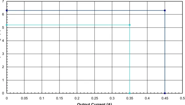
0 1 2 3 4 5 6 7 0 0.05 0.1 0.15 0.2 0.25 0.3 0.35 0.4 0.45 0.5
Output Current (A)
Out
put
Vol
tage (
V)
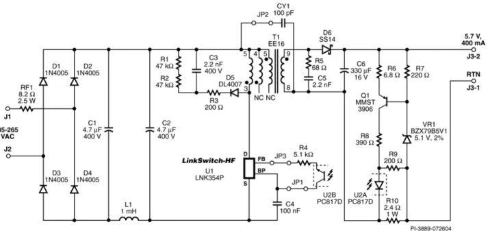
3 Schematic
4 Circuit
Description
This circuit is configured as a flyback topology power supply utilizing the LNK354P. Secondary side constant voltage (CV) and constant current (CC) feedback circuitry provides characteristics required for battery charging applications.
4.1 Input EMI Filtering
The AC input voltage is rectified by input bridge D1 – D4. The rectified DC is then filtered by the bulk storage capacitors C1 and C2. Inductor L1, C1 and C2 form an input pi filter, which attenuates differential mode conducted EMI.
It is recommended that RF1 be of wire-wound construction to withstand input current surges while the input capacitor charges (metal film type are not recommended), and be compliant with safety flammability hazard requirements. Please consult your safety agency representative for requirements specific to your application.
4.2 LinkSwitch-HF Primary
The LNK354P device U1 integrates the power switching device, oscillator, control, startup, and protection functions. The integrated 700 V MOSFET has excellent switching characteristics allowing operation at the 200 kHz operating frequency.
The rectified and filtered input voltage is applied to the primary winding of T1. The other side of the transformer primary is driven by the integrated MOSFET in U1. Diode D5, C3, R1, R2, and R3 form the primary clamp network. This limits the peak drain voltage due to leakage inductance. Resistor R3 allows the use of a slow, low cost rectifier diode by limiting the reverse current through D5 when U1 turns on. The selection of a slow diode also improves conducted EMI.
To regulate the output, ON/OFF control is used. During normal operation, switching of the power MOSFET is disabled when a current greater than 49 µA is delivered into the FEEDBACK pin. Current lower than this threshold allows a switching cycle to occur terminating when the peak primary current reaches the internal current limit.
Current into the FEEDBACK pin is fed, via optocoupler U2, from the BYPASS pin removing the need for an auxiliary bias winding on the transformer.
4.3 Output Rectification
Output rectification is provided by Schottky diode D6. The low forward voltage provides high efficiency across the operating range. Low ESR capacitor C6 achieves minimum output voltage ripple and noise in a small can size for the rated ripple current specification.
4.4 Output Feedback
the bias current through VR1 (~2.7 mA). When the output voltage exceeds the threshold voltage determined by Q1 and VR1, Q1 is turned on and current flows through the LED of U2. As the LED current increases, the current fed into the FEEDBACK pin increases disabling further switching cycles of U1. At very light loads almost all switching cycles will be disabled, giving a low effective switching frequency and providing low no-load consumption.
Resistors R6 and R8 ensure that the ratings of Q1 are not exceeded during load transients.
Resistors R9 and R10 form the constant current (CC) sense circuit. Above approximately 400 mA, the voltage across the sense resistor exceeds the optocoupler diode forward conduction voltage of approximately 1 V. The current through the LED is therefore determined by the output current and CC control dominates the CV feedback loop.
4.5 Design Aspects for EMI
In addition to the simple input pi filter for differential mode EMI, this design makes use of shielding techniques in the transformer to reduce common mode EMI displacement currents. Resistor R5 and C5 are added to act as a damping network to reduce high frequency transformer ringing.
To return high frequency common mode displacement currents, a small value (100 pF) Y1 safety capacitor is placed across the isolation barrier. This is a small enough value to still meet the design requirement of low leakage current.
These techniques combined with the frequency jitter of LinkSwitch-HF give excellent
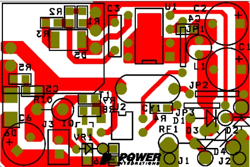
5 PCB
Layout
6 Bill Of Materials
Item Qnty Ref. Des. Value Description Mfg Part Number Manufacturer
1 2 C1, C2 4.7 µF 4.7 4.7 µµF, 400 V, Electrolytic, (8 x 11.5) F, 380 V, Electrolytic, (8 x 11.5) SHD400WV 4.7uF XX380VB4R7M8X11LL Sam Young United Chemi-Con 2 1 C3 2.2nF 2.2 nF, 400 V, Film 222237065222 Vishay (BC Components) 3 1 C4 100 nF 100 nF, 50 V, Ceramic, X7R, 0805 ECU-V1H221KBN Panasonic 4 1 C5 2.2 nF 2.2 nF, 50 V, Ceramic, X7R, 0805 ECJ-2VB1H222K Panasonic 5 1 C6 330 µF 330 72 mµΩF, 16 V, Electrolytic, Very Low ESR, , (8 x 11.5) KZE16VB331MH11LL Nippon Chemi-Con
6 1 CY1 100 pF 100 pF, Ceramic, Y1 440LT10 Vishay
7 4 D1, D2, D3, D4 1N4005 600 V, 1 A, Rectifier, DO-41 1N4005 Vishay
8 1 D5 DL4007 1000 V, 1 A, Rectifier, Glass Passivated, DO-213AA (MELF) DL4007 Diodes Inc
9 1 D6 SS14 40 V, 1 A, Schottky, DO-214AC SS14 Vishay
10 2 J1,J2 PCB Terminal 22 AWG PCB Terminal Hole, 22 AWG N/A N/A
11 1 J3 Output Cable Assembly 6 ft, 0.25 Ω, 2.1 mm connector (custom) 3PH243 Anam Instruments (Korea) 12 3 JP1, JP2, JP3 J Wire Jumper, Non insulated, 22 AWG, 0.4 in 298 Alpha
13 1 L1 1 mH 1 mH, 0.15 A, Ferrite Core SBCP-47HY102B Tokin 14 1 Q1 MMST3906 PNP, Small Signal BJT, 40 V, 0.2 A, SOT-323 MMST3906-7 Diodes Inc 15 2 R1, R2 47 kΩ 47 kΩ, 5%, 1/8 W, Metal Film, 0805 ERJ-6GEYJ473V Panasonic 16 2 R3, R9 200 Ω 200 Ω, 5%, 1/8 W, Metal Film, 0805 ERJ-6GEYJ201V Panasonic 17 1 R4 5.1 kΩ 5.1 kΩ, 5%, 1/8 W, Metal Film, 0805 ERJ-6GEYJ512V Panasonic 18 1 R5 68 Ω 68 Ω, 5%, 1/8 W, Metal Film, 0805 ERJ-6GEYJ680V Panasonic 19 1 R6 6.8 Ω 6.8 Ω, 5%, 1/8 W, Metal Film, 0805 ERJ-6GEYJ6R8V Panasonic 20 1 R7 220 Ω 220 Ω, 5%, 1/8 W, Metal Film, 0805 ERJ-6GEYJ221V Panasonic 21 1 R8 390 Ω 390 Ω, 5%, 1/8 W, Metal Film, 0805 ERJ-6GEYJ391V Panasonic
22 1 R10 2.4 Ω 2.4 Ω, 5%, 1 W, Metal Oxide RSF100JB-2R4 Yageo
23 1 RF1 8.2 Ω 8.2 Ω, 2.5 W, Fusible/Flame-Proof Wire-Wound CRF253-4 5T 8R2 Vitrohm
24 1 T1 EE16 Custom Sil6032 LSLA40331B IM 040 416 11 Hical Li Shin Vogt
25 1 U1 LNK354P LinkSwitch-HF, LNK354P, DIP-8B LNK354P Power Integrations 26 1 U2 PC817D Optocoupler, 80 V, CTR 300-600%, 4-DIP PC817X4, IPC817D Sharp, ISP 27 1 VR1 BZX79-B5V1 5.1 V, 500 mW, 2%, DO-35 BZX79-B5V1 Vishay
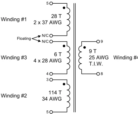
7 Transformer
Specification
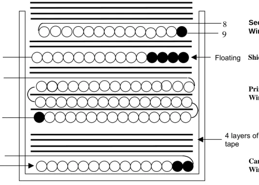
7.1 Electrical Diagram 9 T 25 AWG T.I.W. 28 T 2 x 37 AWG Floating 5 N/C 9 8 6 T 4 x 28 AWG N/C 4 114 T 34 AWG 3 5 Winding #1 Winding #3 Winding #2 Winding #4Figure 5 – Transformer Electrical Diagram.
7.2 Electrical Specifications
Electrical Strength 60 Hz 1 minute, from Pins 3-5 to Pins 6-10 3000 VAC Primary Inductance Pins 3-5, all other windings open, measured at 200 kHz, 0.4 VRMS 916 µH, -/+12%
Resonant Frequency Pins 3-5, all other windings open 900 kHz (Min.) Primary Leakage Inductance Pins 3-5, with Pins 8-9 shorted, measured at 200kHz, 0.4 VRMS 75 µH (Max.)
7.3 Materials
Item Description [1] Core: PC40EE16-Z, TDK or equivalent Gapped for AL of 70 nH/T2
[2] Bobbin: EE16 Horizontal 10 pin [3] Magnet Wire: #37 AWG [4] Magnet Wire: #34 AWG [5] Magnet Wire: #28 AWG
[6] Triple Insulated Wire: #25 AWG.
[7] Tape: 3M 1298 Polyester Film, 2.0 mils thick, 8.4 mm wide
7.4 Transformer Build Diagram Floating Floating 5 Primary Winding Secondary Winding Shield 4 layers of tape Cancellation Winding 3 4 8 9 5
Figure 6 – Transformer Build Diagram.
7.5 Transformer Construction
First Winding - Cancellation
Primary pin side of the bobbin oriented to left-hand side. Start at Pin 8 temporarily. Wind 28 bifilar turns of item [3] from right to left. Wind with tight tension across entire bobbin evenly and leave the finish end free. Bend the free end 90° and draw the wire across the bobbin window cutting in the center of the bobbin. Move start end of winding from Pin 8 to Pin 5.
Insulation 4 Layers of tape [6] for insulation. Second Winding -
Primary
Start at Pin 3 wind 38 turns of item [4] from left to right. Add one layer of tape. Wind another 38 turns from right to left. Add one layer of tape. Wind 38 turns in third layer from left to right. Wind with tight tension across entire bobbin evenly. Finish at Pin 5.
Insulation 2 Layers of tape [6] for insulation. Third Winding -
Shield
Start at Pin 8 temporarily, wind 6 quadfilar turns of item [5]. Wind from right to left with tight tension in a single uniform layer across entire width of bobbin. Finish on Pin 4. Cut start end at Pin 8 ensuring uniformity of winding and tape down in place.
Insulation 2 Layers of tape [7] for insulation.
Fourth Winding Start at Pin 9, wind 9 turns of item [6] from right to left. Wind uniformly, in a single layer across entire bobbin width. Finish on Pin 8. Outer insulation 3 Layers of tape [7] for insulation.
Core Assembly Assemble and secure core halves.
8 Transformer
Design
Spreadsheet
ACDC_LinkSwitch-HF_060904; Rev1-1; Copyright Power Integrations Inc. 2004
INPUT INFO OUTPUT UNIT
ACDC_HF_060904_Rev1-1.xls; LinkSwitch-TN_HF Continuous/Discontinuous Flyback Transformer Design Spreadsheet
ENTER APPLICATION VARIABLES
VACMIN 85 Volts Minimum AC Input Voltage
VACMAX 265 Volts Maximum AC Input Voltage
fL 50 Hertz AC Mains Frequency
VO 5.7 Volts Output Voltage
IO 0.4 Amps Power Supply Output Current
CC Threshold Voltage 1.04 Volts Voltage drop across sense resistor. For CV only circuits enter "0"
PO 2.696 Watts Output Power
n 0.57 Efficiency Estimate. For CV only designs enter 0.7 if no better data available
Z 0.75 Loss Allocation Factor
tC 3 mSeconds Bridge Rectifier Conduction Time Estimate
CIN 9.4 uFarads Input Capacitance
ENTER LinkSwitch-HF VARIABLES
LinkSwitch-HF LNK354 Universal 115 Doubled/230V
Chosen Device LNK354 Power
Out 4.5 W 5 W
ILIMITMIN 0.233 Amps Minimum Current Limit
ILIMITMAX 0.268 Amps Maximum Current Limit
fS 186000 Hertz Minimum Device Switching Frequency
fS Full Load 178750 178750 Hertz
Maximum switching frequency at full load and LP min. For maximum power capability enter 186 kHz (fs_min), reducing this value will reduce EMI but lower power capability
VOR 91 91 Volts Reflected Output Voltage
VDS 10 Volts LinkSwitch-HF on-state Drain to Source Voltage VD 0.45 0.45 Volts Output Winding Diode Forward Voltage Drop
KP 1.15 Ripple to Peak Current Ratio (0.6<KRP<1.0 : 1.0<KDP<6.0)
ENTER TRANSFORMER CORE/CONSTRUCTION VARIABLES
Core Type EE16 EE16 User-Selected transformer core
Core EE16 P/N: PC40EE16-Z
Bobbin EE16_BOBBIN P/N: EE16_BOBBIN
AE 0.192 cm^2 Core Effective Cross Sectional Area
LE 3.5 cm Core Effective Path Length
AL 1140 nH/T^2 Ungapped Core Effective Inductance
BW 8.6 mm Bobbin Physical Winding Width
M 0 mm Safety Margin Width (Half the Primary to Secondary Creepage Distance)
L 3 Number of Primary Layers
NS 9 9 Number of Secondary Turns
DC INPUT VOLTAGE PARAMETERS
VMIN 90 Volts Minimum DC Input Voltage
VMAX 375 Volts Maximum DC Input Voltage
CURRENT WAVEFORM SHAPE PARAMETERS
DMAX 0.54 Maximum Duty Cycle
IAVG 0.05 Amps Average Primary Current
IP 0.23 Amps Minimum Peak Primary Current
IR 0.23 Amps Primary Ripple Current
TRANSFORMER PRIMARY DESIGN PARAMETERS
LP 916 uHenries Typical Primary Inductance. +/- 12% LP_TOLERANCE 12 % Primary inductance tolerance
NP 114 Primary Winding Number of Turns
ALG 71 nH/T^2 Gapped Core Effective Inductance
BM Caution 1298 Gauss !!! Caution. Flux densities above ~ 1250 Gauss may produce audible noise. Verify with dip varnished sample transformers. Increase NS to greater than or equal to 10 turns or increase VOR
BAC 649 Gauss AC Flux Density for Core Loss Curves (0.5 X Peak to Peak)
ur 1654 Relative Permeability of Ungapped Core
LG 0.32 mm Gap Length (Lg > 0.1 mm)
BWE 25.8 mm Effective Bobbin Width
OD 0.23 mm Maximum Primary Wire Diameter including insulation INS 0.05 mm Estimated Total Insulation Thickness (= 2 * film thickness)
DIA 0.18 mm Bare conductor diameter
AWG 34 AWG Primary Wire Gauge (Rounded to next smaller standard AWG value) CM 40 Cmils Bare conductor effective area in circular mils
CMA 466 Cmils/Amp Primary Winding Current Capacity (200 < CMA < 500)
TRANSFORMER SECONDARY DESIGN PARAMETERS Lumped parameters
ISP 2.95 Amps Peak Secondary Current
ISRMS 1.02 Amps Secondary RMS Current
IRIPPLE 0.94 Amps Output Capacitor RMS Ripple Current
CMS 205 Cmils Secondary Bare Conductor minimum circular mils
AWGS 26 AWG Secondary Wire Gauge (Rounded up to next larger standard AWG value) DIAS 0.41 mm Secondary Minimum Bare Conductor Diameter
ODS 0.96 mm Secondary Maximum Outside Diameter for Triple Insulated Wire INSS 0.27 mm Maximum Secondary Insulation Wall Thickness
VOLTAGE STRESS PARAMETERS
VDRAIN 586 Volts Maximum Drain Voltage Estimate (Includes Effect of Leakage Inductance) PIVS 35 Volts Output Rectifier Maximum Peak Inverse Voltage
TRANSFORMER SECONDARY DESIGN PARAMETERS (MULTIPLE OUTPUTS) 1st output
VO1 5.7 Volts Output Voltage (if unused, defaults to single output design)
IO1 0.473 Amps Output DC Current
PO1 2.70 Watts Output Power
VD1 0.45 Volts Output Diode Forward Voltage Drop
NS1 8.34 Output Winding Number of Turns
ISRMS1 1.210 Amps Output Winding RMS Current IRIPPLE1 1.11 Amps Output Capacitor RMS Ripple Current PIVS1 33 Volts Output Rectifier Maximum Peak Inverse Voltage CMS1 242 Cmils Output Winding Bare Conductor minimum circular mils AWGS1 26 AWG Wire Gauge (Rounded up to next larger standard AWG value) DIAS1 0.41 mm Minimum Bare Conductor Diameter
ODS1 1.03 mm Maximum Outside Diameter for Triple Insulated Wire
2nd output
VO2 Volts Output Voltage
IO2 Amps Output DC Current
PO2 0.00 Watts Output Power
VD2 Volts Output Diode Forward Voltage Drop
NS2 0.00 Output Winding Number of Turns
ISRMS2 0.000 Amps Output Winding RMS Current IRIPPLE2 0.00 Amps Output Capacitor RMS Ripple Current PIVS2 0 Volts Output Rectifier Maximum Peak Inverse Voltage CMS2 0 Cmils Output Winding Bare Conductor minimum circular mils AWGS2 N/A AWG Wire Gauge (Rounded up to next larger standard AWG value)
DIAS2 N/A mm Minimum Bare Conductor Diameter
3rd output
VO3 Volts Output Voltage
IO3 Amps Output DC Current
PO3 0.00 Watts Output Power
VD3 Volts Output Diode Forward Voltage Drop
NS3 0.00 Output Winding Number of Turns
ISRMS3 0.000 Amps Output Winding RMS Current
IRIPPLE3 0.00 Amps Output Capacitor RMS Ripple Current PIVS3 0 Volts Output Rectifier Maximum Peak Inverse Voltage CMS3 0 Cmils Output Winding Bare Conductor minimum circular mils AWGS3 N/A AWG Wire Gauge (Rounded up to next larger standard AWG value)
DIAS3 N/A mm Minimum Bare Conductor Diameter
ODS3 N/A mm Maximum Outside Diameter for Triple Insulated Wire
9 Performance
Data
All measurements performed at room temperature, 60 Hz input frequency. A DC output cable was not included.
9.1 Efficiency
Figure 7 – Efficiency vs. Output Current (CV), Room Temperature, 60 Hz.
40% 45% 50% 55% 60% 65% 0 0.05 0.1 0.15 0.2 0.25 0.3 0.35 0.4 0.45
Output Load (A)
Efficien cy 90 VAC 115 VAC 230 VAC 265 VAC
0 0.05 0.1 0.15 0.2 0.25 0.3 50 100 150 200 250 300
Input Voltage (VAC)
Input Power (W)
Figure 8 –Zero Load Input Power vs. Input Line Voltage, Room Temperature, 60 Hz.
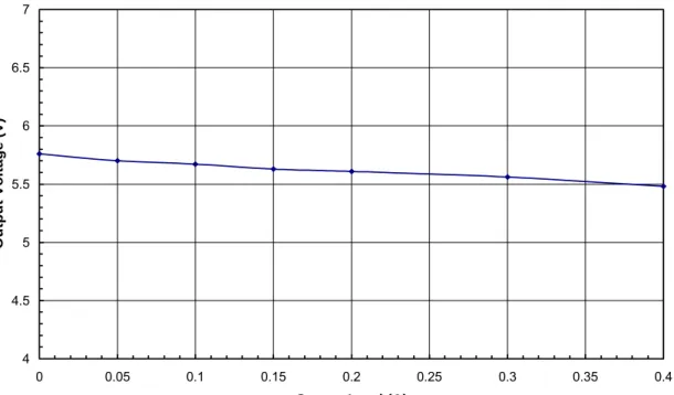
9.3 Regulation
9.3.1 CV and CC Output Characteristics
No measurable difference was seen over line voltage variation.
0 1 2 3 4 5 6 7 0 0.05 0.1 0.15 0.2 0.25 0.3 0.35 0.4 0.45 0.5
Output Current (A)
Output Voltage (V)
9.3.2 Load Regulation in CV 4 4.5 5 5.5 6 6.5 7 0 0.05 0.1 0.15 0.2 0.25 0.3 0.35 0.4
Output Load (A)
Output Volta
g
e
(V)
10 Thermal Performance
Temperature of key components was recorded using a T-type thermocouple. Thermocouples were soldered directly to LNK354P SOURCE pin and cathode of output rectifier. Thermocouples were glued to the output capacitor and transformer external core/winding surfaces.
The unit was operated at full load in free convection in a thermal chamber inside an additional enclosure to eliminate airflow. The ambient was measured in the additional enclosure and maintained at 40 °C.
Temperature (°C)
Item 85 VAC 265 VAC
Ambient 40 40
LNK354P (U1) 94 96
Transformer (T1) 80 82
Output Rectifier (D6) 67 64
Output Capacitor (C6) 60 58
For reference an infrared thermograph was taken with the unit operating at room ambient showing the relative temperature rise of the key supply components.
11 Line Surge
SurgeVoltage Phase Angle
Generator
Impedance Number of Strikes Test Result
2 kV 90° 2 Ω 10 PASS
12 Waveforms
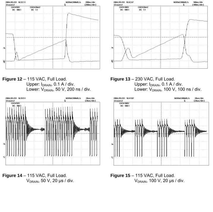
12.1 Drain Voltage and Current, Normal Operation
Figure 12 – 115 VAC, Full Load.
Upper: IDRAIN, 0.1 A / div.
Lower: VDRAIN, 50 V, 200 ns / div.
Figure 13 – 230 VAC, Full Load.
Upper: IDRAIN, 0.1 A / div.
Lower: VDRAIN, 100 V, 100 ns / div.
Figure 14 – 115 VAC, Full Load. VDRAIN, 50 V, 20 µs / div.
Figure 15 – 115 VAC, Full Load. VDRAIN, 100 V, 20 µs / div.
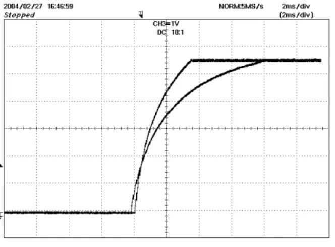
12.2 Output Voltage Start-up Profile
Startup into resistive full load and no-load was verified. Load resistor was sized at 13 Ω
to maintain 300 mA under steady-state conditions.
Figure 16 – Start-up Profile115 VAC. Fast trace is no load rise time. Slower trace is maximum load (13 Ω) 1 V, 2 ms / div.
Figure 17 – Start-up Profile 230 VAC. Fast trace is no load rise time.
Slower trace is maximum load (13 Ω)
1 V, 2 ms / div.
12.3 Drain Voltage and Current Start-up Profile
Figure 18 – 90 VAC Input and Maximum Load (Resistive Load).
Upper: 200 V & 500 µs/ div. Lower: VDRAIN, IDRAIN, 0.1 A / div.
Figure 19 – 265 VAC Input and Maximum Load (Resistive Load).
Upper: 200 V & 500 µs/ div. Lower: VDRAIN, IDRAIN, 0.1 A / div.
12.4 Load Transient Response (75% to 100% Load Step)
Figure 20 – Transient Response, 115VAC,
75-100-75% Load Step. Upper:. VOUT 20 mV, 1 ms / div.
Lower: IOUT, 0.1 A / div.
Figure 21 – Transient Response, 230VAC,
75-100-75% Load Step. Upper: VOUT, 20 mV, 1ms / div.
12.5 Output Ripple Measurements
12.5.1 Ripple Measurement Technique
For DC output ripple measurements, a modified oscilloscope test probe must be utilized in order to reduce spurious signals due to pickup. Attach probe with end cap and ground clip removed to circuit shown below which is attached to end of output cable.
The 5125BA probe adapter is affixed
Probe Ground
Probe Tip
Figure 22– Oscilloscope Probe Prepared for Ripple Measurement (End Cap and Ground Lead Removed).
RCABLE (0.15 Ω) DA DB RBATTERY (0.44 Ω) CA 10,000 µF RLOAD (13 Ω)
12.5.2 Measurement Results
Figure 24 – Output Ripple, 115 VAC, Full Load.
20 µs, 50 mV / div.
Figure 25 – Output Ripple, 230 VAC, Full Load.
13 Conducted EMI
Conducted emissions tests were completed at 115 VAC and 230 VAC at full load, 5.5 V / 400 mA. Measurements were completed with Artificial Hand connection and floating DC output load resistor. An output DC cable was included.
Composite EN55022B / CISPR22B conducted limits are shown. 13.1 115 VAC Input, Full Load
Line Neutral
Artificial Hand Connected to Output Return Artificial Hand Connected to Output Return
13.2 230 VAC Input, Full Load
Line Neutral
Artificial Hand Connected to Output Return Artificial Hand Connected to Output Return
14 Appendix A – Design Modification Required To Remove Y Capacitor
In some applications where extremely low leakage current is required, it may be necessary to remove the Y capacitor (CY1) that bridges the primary-to-secondary isolation barrier.
In order to achieve this while still meeting conducted and radiated EMI requires re-optimization of the transformer. As with all no Y capacitor transformer designs, the mechanical arrangement and relative spacing of the windings has a large impact on the EMI performance of the supply. Therefore ensure that transformers are wound consistently to ensure repeatable EMI performance.
14.1 No Y capacitor Transformer Specification
14.1.1 Electrical Diagram 9 T 25 AWG T.I.W. 17 T 2 x 32 AWG Floating 5 N/C 9 8 7 T 3 x 28 AWG N/C 4 114 T 36 AWG 3 5 Winding #1 (Cancellation) Winding #3 (Shield) Winding #2 (Primary) Winding #4 (Secondary)
Denotes mechanical start of reverse wound winding where electrical phasing and mechanical start are not the same
14.1.2 Electrical Specifications
Electrical Strength 60Hz 1minute, from Pins 3-5 to Pins 6-10 3000 VAC Primary Inductance Pins 3-5, all other windings open, measured at 200 kHz, 0.4 VRMS 916 µH, -/+12% Resonant Frequency Pins 3-5, all other windings open 900 kHz (Min.) Primary Leakage Inductance Pins 3-5, with Pins 8-9 shorted, measured at
14.1.3 Winding Instructions
WD1 Cancellation
Winding
Primary pin side of the bobbin oriented to left-hand side. Add 1 layer of item [7] to the secondary side. Start at Pin 5. Wind 17 bifilar turns of item [3] from right to left. Wind with tight tension across entire bobbin evenly. Cut the ends of the bifilar and leave floating.
Insulation 4 Layers of tape [8] for insulation. WD#2
Primary winding Apply 1 layer of item [7] to the secondary side. Start at Pin 3. Wind 40 turns of item [4] from left to right. Add 1 layer of item [8] and 1 layer of item [7] to the secondary side. Wind another 40 turns from right to left. Add 1 layer of item [8] and 1 layer of item [7] to the secondary side. Wind 34 turns in third layer from left to right. Wind with tight tension across entire bobbin evenly. Finish at Pin 5.
Insulation 2 Layers of tape [8] for insulation. WD #3
Shield Winding Start at Pin 8 temporarily, wind 7 trifilar turns of item [5]. Wind from right to left with tight tension. Wind uniformly, in a single layer across entire width of bobbin. Finish on Pin 4. Cut the lead of the starting end and ensure that the void area around the starting end is entirely covered with the cut end. Tape down in place.
Insulation 2 Layers of tape [8] for insulation. WD #4
Secondary Winding
Reverse orientation of bobbin such that secondary pin side is to the left- hand side. Start at Pin 8, wind 9 turns of item [6] from right to left. Wind uniformly, in a single layer across entire bobbin evenly. Finish on Pin 9. Outer Insulation 3 Layers of tape [8] for insulation.
Core Assembly Assemble and secure core halves using item [9].
Core Grounding Solder 1 end of item [10] to Pin 5. Wrap 2 turns around entire transformer making sure that wire is in contact with cores. Terminate end to Pin 5.
Varnish Dip Varnish, item [11]
14.1.4 Materials
Item Description [1] Core: PC40EE16-Z, TDK or equivalent Gapped for AL of 192 nH/T2
[2] Bobbin: EE16 Horizontal 10 pin
[3] Magnet Wire: #32 AWG [4] Magnet Wire: #36 AWG [5] Magnet Wire: #28 AWG
[6] Triple Insulated Wire: #25 AWG.
[7] Tape: 3M # 44 Polyester web. 1.5 mm wide
[8] Tape: 3M 1298 Polyester Film, 2.0 mils thick, 8.0 mm wide [9] Tape: 3M 1298 Polyester Film, 2.0 mils thick, 3.0 mm wide [10] Solid Wire: #28 AWG
14.1.5 Transformer Build Diagram 1.5 mm 1.5 mm 5 5 3 4 9 8 N.C. (Floating) N.C. 4 layers of tape 3 layers of tape Secondary Shield Primary
Cancellation Tape margin
Denotes mechanical start of winding where mechanical start and electrical phase are different Denotes mechanical start and electrical phase of winding where they are the same
14.2 EMI Results
Both conducted and radiated EMI results with the revised transformer and CY1 removed showed excellent margin to respective standards. Tests were performed on both line and neutral (conducted) with the output return connected to the artificial hand input of the LISN (line impedance stabilization network). The red trace represents EMI measured with a quasi peak detector and the blue an average detector. These results should be below the respective limit line of the same color.
Radiated results gave a margin of > 6dB.
15 Revision History
Date Author Revision Description & changes
01-Mar-04 AO 0.1 First Draft
01-Apr-04 0.2 Transformer and layout change
05-Apr-04 PV 0.3 Applied correct template, updated circuit description
08-Apr-04 PV 0.4 Reinserted Figure 4 (didn’t printout)
28-Apr-04 AO 0.5 Updated BOM, Spreadsheet, Schematic and Transformer
02-May-04 PV 0.6 4.3: Change R2 to R3, replace terminated with disabled
4.4: Added 1 V opto threshold 6: Corrected description of D6 Fig 4: Added filar to diagram 20-May-04 AO 0.7 Added output characteristic spec 27-May-04 PV 0.8 Updated PCB layout, charts corrected 16-June-04 PV 0.81 R10 part number corrected
Figure 2 updated (Q1 shown as NPN not PNP)
24-June-04 PV 0.9 Reinserted final spreadsheet
For the latest updates, visit our website:www.powerint.com
Power Integrations may make changes to its products at any time. Power Integrations has no liability arising from your use of any information, device or circuit described herein nor does it convey any license under its patent rights or the rights of others. POWER INTEGRATIONS MAKES NO WARRANTIES HEREIN AND SPECIFICALLY DISCLAIMS ALL WARRANTIES INCLUDING, WITHOUT LIMITATION, THE IMPLIED WARRANTIES OF MERCHANTABILITY, FITNESS FOR A PARTICULAR PURPOSE, AND NON-INFRINGEMENT OF THIRD PARTY RIGHTS.
PATENT INFORMATION
The products and applications illustrated herein (including circuits external to the products and transformer construction) may be covered by one or more U.S. and foreign patents or potentially by pending U.S. and foreign patent applications assigned to Power
Integrations. A complete list of Power Integrations’ patents may be found at www.powerint.com.
The PI Logo, TOPSwitch,TinySwitch, LinkSwitch, DPA-Switch and EcoSmart are registered trademarks of
Power Integrations. PI Expert and PI FACTS are trademarks of Power Integrations. © Copyright 2004, Power Integrations.
Power Integrations Worldwide Sales Support Locations WORLD HEADQUARTERS
5245 Hellyer Avenue, San Jose, CA 95138, USA Main: +1-408-414-9200 Customer Service: Phone: +1-408-414-9665 Fax: +1-408-414-9765 e-mail: [email protected] GERMANY Rueckertstrasse 3, D-80336, Munich, Germany Phone: +49-895-527-3910 Fax: +49-895-527-3920 e-mail: [email protected] JAPAN Keihin-Tatemono 1st Bldg. 12-20 Shin-Yokohama, 2-Chome, Kohoku-ku, Yokohama-shi, Kanagawa 222-0033, Japan Phone: +81-45-471-1021 Fax: +81-45-471-3717 e-mail: [email protected] TAIWAN
5F-1, No. 316, Nei Hu Rd., Sec. 1 Nei Hu Dist.
Taipei, Taiwan 114, R.O.C. Phone: +886-2-2659-4570 Fax: +886-2-2659-4550 e-mail: [email protected] CHINA (SHANGHAI) Rm 807-808A, Pacheer, Commercial Centre, 555 Nanjing West Road, Shanghai, 200041, China Phone: +86-21-6215-5548 Fax: +86-21-6215-2468 e-mail: [email protected]
INDIA (TECHNICAL SUPPORT)
Innovatech 261/A, Ground Floor 7th Main, 17th Cross, Sadashivanagar Bangalore 560080 Phone: +91-80-5113-8020 Fax: +91-80-5113-8023 e-mail: [email protected] KOREA RM 602, 6FL
Korea City Air Terminal B/D, 159-6, Samsung-Dong, Kangnam-Gu, Seoul, Korea Phone: +82-2-2016-6610 Fax: +82-2-2016-6630 e-mail: [email protected]
UK (EUROPE & AFRICA HEADQUARTERS)
1st Floor, St. James’s House East Street
Farnham, Surrey GU9 7TJ United Kingdom Phone: +44 (0) 1252-730-140 Fax: +44 (0) 1252-727-689 e-mail: [email protected] CHINA (SHENZHEN) Room 2206-2207, Block A, Electronics Science & Technology Bldg.,
2070 Shennan Zhong Road, Shenzhen, Guangdong, China, 518031 Phone: +86-755-8379-3243 Fax: +86-755-8379-5828 e-mail: [email protected] ITALY
Via Vittorio Veneto 12, Bresso Milano, 20091, Italy Phone: +39-028-928-6001 Fax: +39-028-928-6009 e-mail: [email protected] SINGAPORE 51 Newton Road, #15-08/10 Goldhill Plaza, Singapore, 308900 Phone: +65-6358-2160 Fax: +65-6358-2015 e-mail: [email protected] APPLICATIONS HOTLINE World Wide +1-408-414-9660 APPLICATIONS FAX World Wide +1-408-414-9760