STRUCTURE AND WEAR RESISTANCE PROPERTIES OF
ELECTROLESS Ni-P ALLOY AND Ni-P-SiC COMPOSITE
COATINGS
T. Y. Soror
[a,b]Keywords: Ni-P plating solution; SiC particles; composite coatings; steel; heat treatment
To verify the relationship between the properties of composite coatings prepared on steel and the SiC content of electroless Ni-P-SiC composite coatings. Systematic experiments have been conducted to study the possibility of incorporating solid SiC particles in Ni-P matrix. Kinetics of Ni-P plating reveal that the rate of deposition was found to increase linearly with time. The reduction process of nickel ions by hypophosphite was completely hindered at pH < 2and the minimum temperature at which the bath can be practically operated was about 65 ˚C. The mode of deposition of Ni-P film has been explored in the light of deposition condition. XRD analysis of the as- plated and heat – treated samples revealed the existence of crystalline Ni3P phases for the heat – treated alloy. Finally a component electroless
Ni-P-SiC composite plating process producing a high wear resistance of the coating.
*Corresponding Authors
*E-mail: [email protected]
[a] Chemistry Department Faculty of Science Qassim University KSA
[b] Chemistry Department Faculty of Science Cairo University Egypt.
Introduction
It is well known that electroless deposited nickel – phosphorus (Ni-P) coatings have been widely used for corrosion protection applications in a variety of environment because of their particular properties such as anticorrosive property wear resistance paramagnetic characteristics hardness and electrocatalytic activity of hydrogen evolution.1-3 A large number of investigations have been
reported that the capability of Ni-P coatings could be well improved via electroless co-deposition process which was combined with particals as a rainforcing phase into the Ni-P matrix to form fuctional composite coatings4.The traditional
electroless composite coatings have been prepared by adding micrometer particles to an electroless bath such as SiC BN PTFE and diamond.5-9 The codeposition to a large
extent improves the mechnical and tribological properties of Ni-P coatings.10-13 Such coatings with a high corrosion
resistance wear resistance and uniform coating thichness have found wide applications in industries of aviation aerospace electronics petroleum machinery textiles and automotives.14.15 These properties have been responsible for
the development of autocatalytic nickel deposition over the last years.16-20 Currently little efforts could be found in
literature on wear resistance of Ni-P –SiC composite coatings.21.22
Finally a component electroless Ni-P-SiC composite plating process producing a high wears resistance of the coating. The objective of this work is to obtain a process and plating solution of preparing Ni-P-SiC composite coatings of excellent performance of wear resistance.
Experimental section
Materials
All the chemicals used for plating bath preparations were of reagent grade in particular sodium hypophosphite which is BDH product. Sample substrates used were low carbon steel sheets 0.8mm thick of the following analysis: 0.093 % carbon 0.532 % manganese 0.007 % sulfur and 0.007 % phosphorus.
Composite coatings were formed when SiC particles with diameters 1-3 µm were mixed with components of electroless nickel phosphorus bath.
Bath composition and operating conditions
For electroless nickel deposition on steel substrates the acetate bath23 was selected which has the following
composition:
NiSO4.6H2O 35 g L-1
NaH2PO2.H2O 10 g L-1
Na3C6H5O7 15 g L-1
CH3COOONa .3H2O 5 g L-1
The pH value of the as prepared bath is 6 .Adjustment of the pH was carried out by either NaOH or H2SO4. Reaction
temperature was maintained constant thermostatically at 95 ± 1˚C. The ratio of the solution volume to the area of specimen to be plated was taken into consideration (250 mL for 12 cm3).When SiC was used we add 15 g L-1 with
Surface pretreatment
The specimens were abraded with fine emery paper (600-girt) cleaned by wet calcium oxide powder rinsed with water and dried.
Metallographic examination
For metallographic examination measurement of coating thickness and micro hardness determination require standard sample preparation. The coated specimen is mounted vertically in bakelite then ground and polished according to the usual metallographic procedure. The sample was etched in a reagent that emphasizes the contrast between the base metal and the coating. A solution of the following composition is used at room temperature:
Soln. (A): Ammonium persulphate 10 g/l00 mL
Soln.(B): Sodium cyanide 10 g/100 mL
Equal volumes of the two solutions were mixed and the etchant was applied to the specimen by swabbing for 30-60s.
Hardness measurement
Microhardness indentation technique was used to measure the hardness of coating layers. The technique consists of applying a specified load (100 g) to an identor of specific geometry.The geometry of the indentation remaining in the metal after load removal is a measure of hardness. The Vickers hardness number (VHN) was determined from the average of ten readings.
Wear resistance measurement
The wear test of these coatings was made by hanging it in a steel rod fitted on a motor stirrer and placed in glass container filled with 4kg sand to 2kg water . The tests were carried out at a speed of 500rpm .The wear of the coating was evaluated from measuring the loss in weight as a function of time.
Results and discussion
Kinetics of electroless nickel deposition
The influence of the different species present in the solution and the operating conditions on the kinetics of electroless nickel deposition was studied using sodium citrate as a complexing agent.
Plating rate and factors affecting it
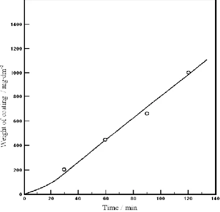
Figure 1 shows the variation of plating weight expressed in mg\dm2 with time. The metal deposition starts with an
initial slow rate followed by a period of regular deposition with time .The initial slow rate can be considered as due to destruction of the natural oxide film covering the surface of steel . Once this film is attacked and active sites are nucleated the catalytic deposition of nickel increases and the reaction proceeds at a constant rate of 8.88 mg dm-2 min-1.
Figure 1. Variation of coating weight with plating time. pH-value
The pH value of the solution affects greatly the kinetics of the deposition process. Figure 2 illustrates the effect of pH– value on the deposition rate. The plating rate increases with increase of pH and reaches a maximum at pH around 6 and then falls again .The relation indicates that the reduction processes was hindered completely at pH value less than 2. The reduction of plating rate in solutions of pH values higher than 6 may be explained on the basis of the decreased ability of solution to maintain the nickel ion in a complex form.
Figure 2. Effect of pH-value on the rate of deposition.
Temperature
Figure 3. Effect of temperature on the rate of deposition.
Mode of deposition of EN
The initial deposition stages of EN-plated film play an important role for the build–up of the overall coating .from which .of course .its functional properties originate.
Figure 4. Arrhinius plot for nickel deposition.
For the study of the mode of EN deposition a steel plate sample (10×15 mm) was held in bakelite mold with one surface free for plating. The metal surface is given a mirror like finish by mechanical polishing and then cleaned in the usual way. The whole sample is immersed in the EN bath at 95 ˚C.The sample is periodically removed from the plating solution for optical microscopic examination without etching using polarized light technique. Figures (5a-f) exhibit the mode of the film build – up during the plating process for a period of one hour.
Deposition appears to start at certain active sites(nuclei) on the substrate surface (Fig.5 a) where reduction of nickel atoms takes place. With the progress of deposition greater number of active sites are involved in the reduction process and aggregates of such sites appear on the surface(fig 5b)It should be reminded that on atomic scale aggregates of reduced atoms accumulate on the starting nuclei and they grew in size to be seen on microscopic scale. The growth of aggregates occurs in two dimensions vertical and horizontal forming hemispheres or parts of spheres of Ni-P film. When seen under microscope it appears as centered circles
expressing reflected light on the top and on the periphery of the hemispheres (arrows in Fig 5c).The hemispherical growth of Ni-P with centered nuclei was similarly identified by Marton and Schlesinger24.The isotropic growth of
adjacent hemispheres will lead to island formation (Fig 5d and e) and the periphery may naturally overlap. The ultimate of the growth process is the formation of a continuous film (Fig. 5f) with un-identified periphery of any of the forming spheres.
Fig. (5a-f) Photomicrographs of the progress of Ni-P deposition showing: a) Active sites on substrate surface, b) Aggregates of deposited nuclei, c) Hemispherical growth of Ni-P with centered nuclei, d) Island formation of the deposit, e) Islands with periphery overlap and f) Continuous film.
Structure of electroless nickel deposits
The variation of the structure of the deposited coating during plating was studied by metallographic examination .The photomicrograph Fig. 6 of the etched cross section of electroless nickel coating shows that the deposits are characterized by lamellar structure of narrow striations formed by variations in the degree of etching.
Figure 6. Cross section of as-deposited electroless Ni-P (unstirred solution) .
These are usually attributed to variations in the phosphorous content of the deposit2-5An inverse correlation
exists between the degree of etching and (p) content of the
a
b
c
d
e
deposit. A white band being more resistant to etching contains greater (p) percentage while the dark band is less in (p) content. This can be attributed to periodic variations of the reduction rate of Ni and P.25 The change is due to PH
alternation in the layer adjacent to solution.26
Figure 7. Microstructure of as-deposited electroless Ni-P (stirred solution) .
Figure 8. Transverse section of heat-treated electroless Ni-p deposits (unstirred solution).
Figure 9. Transverse section of heat-treated electroless Ni-p deposits (stirred solution).
In conclusion, the lamellar structure of EN can be explained in terms of the fact that adsorbed hydrogen will reduce nickel ions preferentially than producing H2 gas until
nickel mono layer is formed .In this case the catalytic activity of the surface is altered by the deposited nickel atoms and H2PO2- will be oxidized on new surface forming
H+ and the process continue to produce Ni-P deposits.
Photomicrograph no.7 represents the microstructure of the coating obtained from a stirred bath. Under this conditions no striations were resolved and the grain size of the deposits are considerably small and the grains acquire spherical form showing homogeneous dispersion of (p) in Ni – matrix. The disappearance of a lamellar deposit in the stirred bath is a direct consequence of the missing diffusion control process.
As this occurs there is no concentration gradient and the ratio between H2PO2-\Ni2+ is altered and therefore no
striations could be formed.
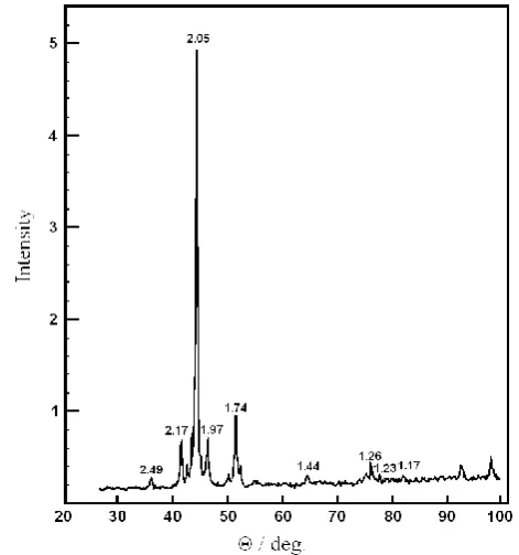
Figure 10. XRD pattern of as-plated EN coating (unstirred solution). .
Figure 11. XRD pattern of heat-plated EN coating (unstirred solution). .
The microstructure of a transverse section of the heat treated electroless Ni-p deposit on carbon steel is presented in figs. 8.9. The change in microstructure is attributed to the formation of the equilibrium phases of Ni and Ni3P as
indicated by X-ray diffraction analysis (Figs10&11). The microstructure of figure 8 stands for the microstructure of which the maximum hardness value (790 VHN) is achievable for the electroless Ni-p deposits. The as–plated sample shows (410VHN) in hardness measurement. On at the other hand XRD of the heat treated samples for unstirred bath at 400˚c gives rise to Ni and Ni3P grains .Nucleation
and growth of Ni3P grains up on heat treatment causes a
Fig. 12 wear resistance characteristics expressed as metal loss with time of friction a) steel substrate, b) Ni-P-Sic composite coating and c) exposed substrate surface .
Wear resistance characteristics
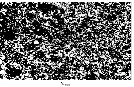
For the measurement of wear resistance the coated samples (25.50.1mm)were rotated tangentially in a sand \ water medium of ratio 4Kg sand \2Kg water condition. The rotation speed was kept constant at 500 rpm and the wear effect is measured in terms of loss in weight expressed as g\h .The results shown in fig 12 .Line (a) indicates a regular rate of metal loss with time 4.9.10-4 g\h for uncoated steel sample .In comparison the results for Ni-P-SiC coating shows a high resistance to wear line (b) for about 1h followed by a steady decrease with the same rate as for steel sample line (c). This indicates that the composite coating enjoys a high wear resistance which prevails till complete loss of the coating within 1 h exposing the base metal after that. Since the wear effect is a surface phenomenon the resistance to wear is largely affected by the amount size and distribution of the carbide particles in the microstructure of the coating. This effect is mostly attributed to the proportion of the surface area occupied by the carbides in the matrix of the coating – photomicrograph of Fig. 13. This high resistance to wear may be also attributed also to the (1000VHN) for heat treated Ni-P-SiC composite coating.
Figure 13.
Photomicrograph of heat treated Ni-P-SiC
(electroless) .
Conclusions
The conclusions obtained from this work can be summarized as follows:
1. The rate of deposition of Ni-P was found to increase linearly with time.
2. The reduction process of nickel ions by hypophosphite is completely hindered at pH<2.
3. The minimum temperature at which the bath can be practically operated is about 65˚C.
4. The lamellar structure (as-plated) Ni–P was explained in terms of the periodic variations of the reduction rates of nickel and phosphorus.
5. XRD analysis of the heat – treated samples indicated the existence of Ni3P phase.
6. The results of wear measurements indicated that the composite coating Ni-P-SiC enjoys a unique high wear resistance compared to the usual Ni-P.
References
1Ger, M. D., Hou, K.H., and Hwang B.J., Mater. Chem. Phys.,
2004, 87, 102.
2Elanszhian, R., Ramamoothy, B., and Kesavan Nair, P., .J. Mater Process. Technol., 2009, 209, 233.
3Ger, M. D., Hou, K. H., Wang, L. M., and Wang, B. J. H., Mater. Chem. Phys., 2003, 77, 755.
4Straffelini, G., Colombo, D., and Molinari, A., Wear, 1999, 236,
179
5Balaraju, J. N., Sankara Narayanan, T. S. N., and Seshadri, S. K., J. Solid State Electrochem., 2001, 5, 1334.
6Balaraju, J. N., and Seshadri, S. K., J. Mater .Sci.Lett., 1998, 17,
1297.
7Leon, O. A., Staia, M. H., and Hintermann. E., Surf. Coat. Technol., 1998, 461, 108-109.
8Ger, M. D., Hou, K. H., and Hwang, B. J., Mater. Chem. Phys.,
2004, 76, 38.
9Reddy, V.V.N., Ramamoothy, B., and Nair, P.K., Wear 2000, 239,
111.
10Grosjean, A., Rezrazi, M., Takadoum, J. and Bercot, P., Surf. Coat. Technol., 2001, 137, 92.
11Apachitei, I., Surf. Coat. Technol., 2002, 149, 263.
12Balaraju, J. N., and Seshadri, S. K., Trans. IMF, 1999, 77, 84. 13Moonir-Vaghefi, S. M., Saatchi, A., and Hejazi, J. Z. Met. Kd.,
1997, 88, 498.
14Jin, J. G., Lee, S. K., and Kim, T. Y., Thin Solid Film, 2004, 466,
272.
15Niwa, D., Takano, N., and Yamada, T., Electrochim.Acta, 2003, 48, 1295.
16Ashassi–Sorkhabi, H., and Rafizadeh., S. H., Surf. Coat. Technol.,
2004, 176, 318-326.
17Rajam, K., and Rajagopal, S. I., Met. Finish, 1990, 88, 77.
18Graham C. J., Electroless Nickel 89 Conference Proceedings Products Finishing Magazine, Cincinatti, OH, 1989 p.1.
19Lu, G., and Zangari, G., Electrochim. Acta,2002, 47, 2969. 20Singh, D., Balasubramaniam, R., Dube, R. K., Corr. Sci., 1995, 8,
581.
21Lin, C. J., and He, J. L., Wear,2005, 259, 154.
22Lin, C. J., Chen, K.C., and He, J. L., Wear, 2006, 261, 1390. 23Brenner, A., and Riddell, G. E., J. Res. Nat. Bur. Stand., 1947, 33,
24Marton J. P., and Schlesinger, M., J. Electrochem. Soc., 1968, 115, 16.
25Graham, A. K., Electroplating Engineering Handbook. 3rd Ed.
New York. Van Nostrand Reinhold Co. 1961, 498.
26Gorbunova, K. M., Laranov, M. V., and Moiseev, V. P., J. Electrochem. Soc., 1973, 120, 613.