FEATURES
High Efficiency: ‡85%
Maximum Output Current: 6A Current Output Noise: 0.05%
High Stability: – 12mA@6A (0.2%) for entire temp. range
Loop Good Indication Fully shielded Compact Size
100 % lead (Pb)-free and RoHS compliant
APPLICATIONS
Driving laser diodes, DPSSL, EDFA, fiber laser, direct diode laser, etc., with low noise and high efficiency.
DESCRIPTION
This laser driver, ATLS6A201D, is an electronic module designed for driving diode lasers by up to 6A constant current with high efficiency, low noise, high reliability, zero EMI, and small package. There are two types: ATLS6A201D and ATLS6A201D-PD, and the latter has a pull-down resistor to the ground. Figure 1.1 shows physical photo of the ATLS6A201D and Figure 1.2 shows the photo of ATLS6A201D-PD.
It provides these functions: laser current control, laser current monitoring, over temperature protection, loop good indication, laser diode status indication, soft start, and shut down.
It comes with a high stability low noise 2.5V voltage reference output which can be used for setting the output current and, at the same time, for the ADCs (Analog to Digital Converters) and/or DACs (Digital to Analog Converters) as the reference voltage.
Warning: This module can only be soldered manually on the board by a solder iron at < 310ºC (590ºF), it cannot go through a reflow oven process.
Figure 1.1. Physical Photo of ATLS6A201D
Figure 1.2. Physical Photo of ATLS6A201D-PD The ATLS6A201D is packaged in a 6 sided metal enclosure, which blocks EMIs (Electro-Magnetic Interferences) to prevent the driver and other electronics from interfering 1each other.
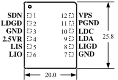
Figure 2. Pin Names and Locations
Figure 2 is the actual sized top view of the ATLS6A201D, which also shows the pin names and locations. Its thickness is 5mm. The pin functions are described in Table 1 below. Table 1. Pin Function Descriptions
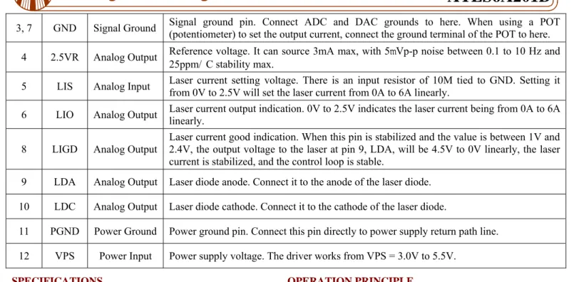
Pin # Name Type Description
1 SDN Digital Input
ATLS6A201D: Shut down control. Negative logic, >1.4V = enable, <0.95V = shut down, normal threshold voltage = 1.2V.
ATLS6A201D-PD: Shut down control. Positive logic, >1.4V = enable, <0.95V = shut down, normal threshold voltage = 1.2V. There is a pull-down resistor of 55K to the ground.
2 LDGD Digital Output
Laser diode good indication. When this pin is high, >2V, the control loop is working properly. When this pin is low, <0.3V, the laser diode is bad, or there is a short or open circuit at the laser diode.
2.5VR 25.8 VPS PGND LDC LDA LIGD GND LDGD GND LIS LIO SDN 1 3 4 5 6 2 12 10 9 8 7 11 20.0
3, 7 GND Signal Ground Signal ground pin. Connect ADC and DAC grounds to here. When using a POT (potentiometer) to set the output current, connect the ground terminal of the POT to here. 4 2.5VR Analog Output Reference voltage. It can source 3mA max, with 5mVp-p noise between 0.1 to 10 Hz and
25ppm/ C stability max.
5 LIS Analog Input Laser current setting voltage. There is an input resistor of 10M tied to GND. Setting it from 0V to 2.5V will set the laser current from 0A to 6A linearly. 6 LIO Analog Output Laser current output indication. 0V to 2.5V indicates the laser current being from 0A to 6A linearly. 8 LIGD Analog Output Laser current good indication. When this pin is stabilized and the value is between 1V and 2.4V, the output voltage to the laser at pin 9, LDA, will be 4.5V to 0V linearly, the laser
current is stabilized, and the control loop is stable.
9 LDA Analog Output Laser diode anode. Connect it to the anode of the laser diode. 10 LDC Analog Output Laser diode cathode. Connect it to the cathode of the laser diode.
11 PGND Power Ground Power ground pin. Connect this pin directly to power supply return path line. 12 VPS Power Input Power supply voltage. The driver works from VPS = 3.0V to 5.5V.
SPECIFICATIONS
Table 2. Characteristics (Tambient = 25 C)
Parameter Value Unit
Laser driver efficiency when
Iout = 6A, Vout = 2.5V, & VPS = 5V. ‡85 % Maximum output current 6 A Low frequency, 0 to 10Hz, output
current noise 20 µA
Stability @ 6A –0.2 %
PWM Frequency 500 KHz
Laser current control signal at LIS 0 ~ 2.5 V LIS control accuracy –0.2 %
Laser current indication signal at LIO 0 ~ 2.5 V LIO indication accuracy –0.2 %
Reference output voltage 2.5 V Output voltage range at LDA 0.85×V0 ~
PS V Power supply voltage range 3.0 ~ 5.5 V Maximum power supply voltage 6 V
Start-up time 4 ms
Typical pull-down current at LDGD 6 mA Operating case temperature -40 ~ 85 C
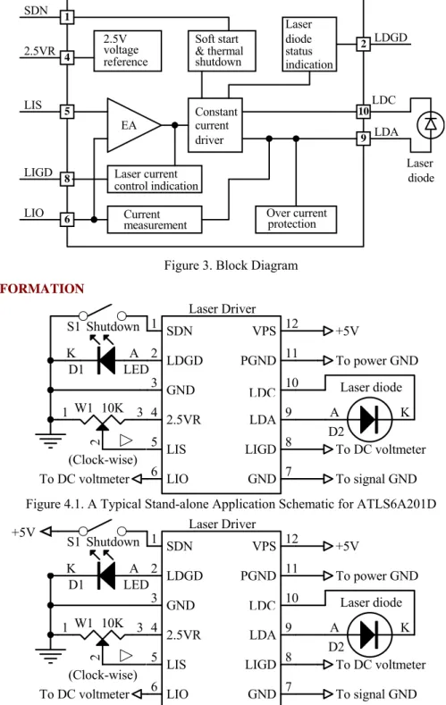
OPERATION PRINCIPLE
The block diagram of the driver is shown in Figure 3. The shut down control circuit accepts signals from 3 sources: external shut down, over current and over temperature signals. When any of these signals is activated, the driver is shut down. Only when none all these 3 signals is activated, a soft start circuit starts enabling the driver stage.
The soft start circuit increases the output current slowly at the start up time and shuts down the current quickly. Thermal shutdown circuit turns the driver off if the junction temperature exceeds 150°C. The driver is released from shutdown automatically when the junction temperature decreases to 10°C below the thermal shutdown trip point, and starts up under control of the soft start circuit. The over current protection circuit turns the driver off if the output current exceeds 10A @ VPS=3V or 12A @ VPS=6V.
The high stability low noise 2.5V voltage reference is provided for setting the output current by setting the LIS’ voltage, and can also be used for the ADCs and/or DACs.
The laser diode status indication circuit monitors laser diode status. When LDGD pin is high, >2V, the control loop is working properly; when this pin goes low, <0.3V, the laser diode is bad, or there is a short or open circuit at the laser diode. The laser current control indication circuit shows the driving status for the output current. When this voltage is between 0.2V to 1.8V, the output voltage on the laser diode is between 4.8V to 0V.
The current measurement circuit monitors the output current and shuts down the driver upon detecting the output current exceeds the pre-set value. It also provides a signal, LIO, indicating the actual laser diode current. The relationship is: Laser current = 2.4 × LIO voltage (A).
driver EA LDA LIS PGND LIO LIGD 9 5 6 8 10 Over current protection Current measurement Laser diode & thermal shutdown Laser diode voltage Constant current 2.5V reference Soft start 2 LDGD SDN 1 2.5VR 4 indication status Laser current control indication
Figure 3. Block Diagram
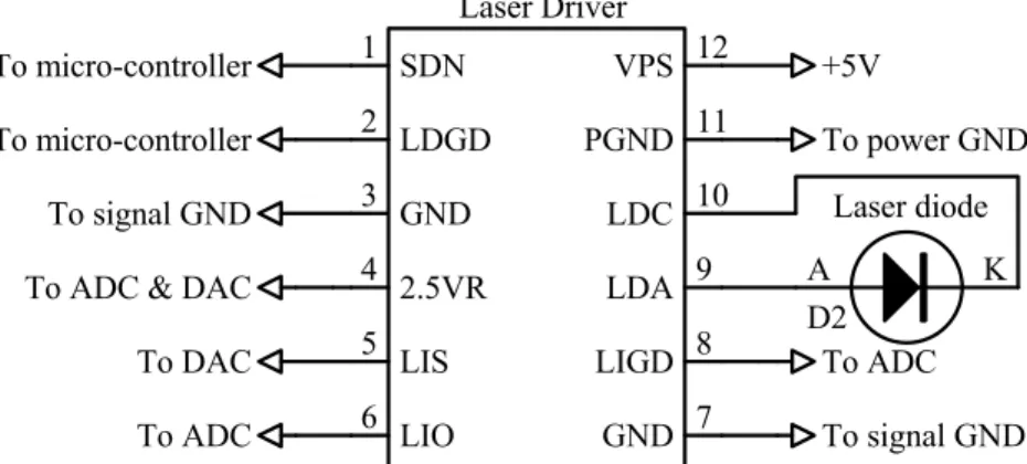
APPLICATION INFORMATION To power GND +5V LIO 6 VPS 12 PGND 10 LIGD 8 LDA 9 GND 3 2.5VR 4 LIS 5 PGND 11 GND 7 LDGD 2 SDN 1 Laser Driver A K Laser diode D2 (Clock-wise) S1 Shutdown A K D1 LED To DC voltmeter To DC voltmeter To signal GND 3 2 1 W1 10K
Figure 4.1. A Typical Stand-alone Application Schematic for ATLS6A201D
To power GND +5V LIO 6 VPS 12 PGND 10 LIGD 8 LDA 9 GND 3 2.5VR 4 LIS 5 PGND 11 GND 7 LDGD 2 SDN 1 Laser Driver A K Laser diode D2 (Clock-wise) S1 Shutdown A K D1 LED To DC voltmeter To DC voltmeter To signal GND 3 2 1 W1 10K
Figure 4.2. A Typical Stand-alone Application Schematic for ATLS6A201D-PD Figure 4.1 and 4.2 show the typical stand-alone application
circuits for ATLS6A201D and ATLS6A201D-PD respectively.
In Figure 4.1, the switch S1 is an external shut down switch, which turns the driver off and on by tiding SDN pin to the ground or releasing it respectively. In Figure 4.2, the switch
S1 is an external shut down switch, which turns the driver off and on by tiding SDN pin to VPS or releasing it respectively. The starting up time delay is about 4mS and the shut down time is about 20µS.
The switch S1 can also be an electronic switch, such as an I/O pin of a micro-driver, with an either open drain or push/pull
LDC
LDC
LDC +5V
output. See Figure 5. For ATLS6A201D, the internal equivalent circuit is a resistor of 100K pulling up this pin to VPS rail. And for ATLS6A201D-PD, the internal equivalent circuit is a resistor of 55K pulling down this pin to GND. When this pin voltage is >1.4V, the driver is enabled; <0.95V, the driver is shut down. Normal threshold voltage = 1.2V.
If not using a switch (S1) to control the laser, leave the SDN pin unconnected.
In Figure 4.1, the LED D1 is used to indicate laser diode status. When LDGD pin is high, >2V, the laser diode control loop is working properly. When LDGD pin is low, <0.3V, the laser diode is bad, or there is a short or open circuit at the laser diode. The LDGD pin can also be connected to a digital input pin of a micro-driver, when software/firmware is utilized in the system. See Figure 5. The equivalent circuit of this pin is a 5K resistor pulling up it to the VPS rail and an open drain FET pulling it down to the ground. The up current can be increased by connecting an external pull-up resistor between VPS and LDGD pins, that is equivalent to paralleling the external resistor with the internal 5K
pull-up resistor. However, the total pull-pull-up resistor should be ≥1.5K @ VPS=5V or ≥1K @ VPS=3.3V, otherwise, the internal open drain FET cannot provide the resistors with enough pull-down current to achieve a low enough potential level for a logic low indication. To calculate the total pull-up resistor, use the equation below:
R_total = (R_internal × R_external)/(R_internal + R_external) where:
R_total is the total pull-up resistor, R_internal is the internal pull-up resistor, R_external is the external pull-up resistor.
The laser diode D2 is connected between LDA and LDC. It is worth mentioning that the power supply return terminal should be connected to the pin 11 PGND and the cathode of the laser diode should be connected to the pin 10 LDC. These 2 pins, 10 and 11, should not be connected together externally and they are connected together internally already by the driver.
Figure 5 shows a typical micro-processor-based application circuit.
To ADC & DAC
To ADC To ADC To micro-controller To signal GND To power GND +5V LIO 6 VPS 12 PGND 10 LIGD 8 LDA 9 GND 3 2.5VR 4 LIS 5 PGND 11 GND 7 LDGD 2 SDN 1 Laser Driver To DAC To signal GND To micro-controller A K Laser diode D2 Figure 5. A Typical Micro-processor-based Application Schematic
Turning the Driver On and Off
The driver can be turned on and off by setting the SDN pin high and low respectively. It is recommended to turn the driver on by this sequence:
To turn on: turn on the power by providing the power supply voltage to the driver on VPS pin, turn on the driver by releasing the SDN pin.
To turn off: turn off the driver by lowering the voltage of SDN pin, turn off the power by stopping the voltage supply on the VPS pin.
When not controlling by the SDN pin: leave it unconnected and turn on and off the driver by the power supply.
Adjusting the Output Current
The output current is set by adjusting W1, which sets input voltages of LIS, pin 5. See Figure 4.1 The output current will be:
I_output = 2.4 · VLIS (A).
LIS can also be set by using a DAC to replace the W1 in Figure 4.1. Make sure that the DAC has low output noise. A RC low pass filtered can be inserted between the W1 output or the DAC output and the LIS pin, for lowering the output noise.
Monitoring the Output Current
The output current of the driver can be monitored by measuring the voltage on the LIO pin. This feature is very useful for micro-driver based system where the ADC is available and monitoring the current in real time is required. This pin provides a very low noise voltage signal and is proportional to the output current:
I_output = 2.4 · VLIO (A).
For example, when the output signal is 2.5V, the output LDC
current is 6A.
LIO can be used to drive an ADC directly, and also be measured by a multi-meter.
Driver Power Consumption
The power consumption of the driver can be calculated by: P_driver = I_input · VPS – I_output · VLDA,
where P_driver is the power consumed by the driver itself; I_output is the output current;
I_input is the power supply’s input current; VPS is the power supply voltage;
VLDA is the voltage across the laser diode;
η = (I_output · VLDA) / (I_input · VPS).
When P_driver of ATLS6A201D exceeds 2.5W, a heat sink is needed to keep the driver’s temperature below certain level, preferably below 85°C. For most applications, the power consumption exceeds 2.5W when the driving is outputting 6A, thus, heat sinking mechanism is needed. The best way for arranging the heat sinking for the driver is as follows: transferring the heat by sandwiching a piece of gap filler material between the top metal surface of ATLS6A201D and the internal metal surface of the final product’s case as shown in Figure 6 below.
Figure 6. Transferring heat by the gap filler
The gap filler material needs to be mechanically elastic and thermally conductive. One of such products is the T-flex 200 filler sheet made by Lairdtech, the available
thickness is between 1mm to 4mm. More detail technical data about this material can be found here: www.lairdtech.com. To reduce the power consumed by the driver, we recommend using a power supply with its voltage barely higher than 1.2 · V_laser_diode_max.
where V_laser_diode_max is the maximum possible laser diode voltage.
For example, for most diode lasers at 6A, the maximum forward voltage across the laser is about 2.7V, thus, use a 3.3V power supply is enough. Using a 3.3V power supply results in a much lower power consumption by the driver than using a 5V power supply.
First Time Power Up
Laser diode is a high value and vulnerable device. Faults in connections and damages done to the driver during soldering process may damage the laser diode permanently.
To protect the laser diode, it is highly recommend to use 3 to 4 regular diodes of >6A to form a “dummy laser” and insert it in the place of the real laser diode, when powering up the driver for the first time. Use an oscilloscope to monitor the LDA voltage at times of powering up and enabling the shutdown pin, and powering down the laser driver and turning off the shutdown pin, and make sure that there is not over-shoot in output voltage at the LDA pin. At the same time, use an ammeter in serious with the dummy laser, to make sure that the output current is correct.
After thorough checking and making sure free of faults in the system, disconnect the dummy laser diode and connect the real laser diode in place.
The driver output voltage range for the laser is between 0 to 0.85 · VPS.
The rise and fall time of this driver is about 15uS. Metal case of final product
PCB board Gap Laser driver
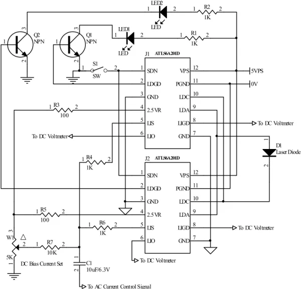
TWO ATLS6A201DS IN PARALLEL
Two laser drivers, ATLS6A201-D, in parallel can generate a maximum 12A current. Meanwhile, there is no interference between the two laser drivers when they are working.
The standard working voltage of ATLS6A201-D is 5V DC, which will be provided to pin 12 of the two drivers by the power supply. Pin 11, PGND, is the power ground pin. Connect this pin to the cathode of the power supply. In Figure 7, the switch S1 is external shut down switch, which can turn on and off the driver by close or open this switch (Closing S1 equals to connecting SDN to the ground). VSDN >1.4V = enable, <0.95V = shut down. If not using S1 to control the laser, leave the SDN pin unconnected.
In Figure 7, the LEDs, D2 and D3, are used to indicate laser diode status. When LDGD pin is high, >2V, the laser diode control loop is working properly; when this pin is low, <0.3V, the laser diode is bad, or there is a short or open circuit at the laser diode. In Figure 7, Pin 3 and pin 7 are the signal source ground. Pin 4 is the 2.5V output reference voltage. Set the LIS output voltage of the two drivers by using W1, a 5K PWM, to control the output current. When adjusting LIS from 0~2.5V, LIO changes from 0~12A linearly. When LIS is 2.5V, the LIO is 12A. When the input LIS is small square signal, observe the waveforms of the input LIS and LIO of the two drivers in the oscilloscope. If the output is good, it means that the two drivers in parallel are working properly. SDN 1 LDGD 2 GND 3 2.5VR 4 LIS 5 LIO 6 GND 7 LIGD 8 LDA9 LDC 10 PGND 11 VPS 12 ATLS6A201D J1 SDN 1 LDGD 2 GND 3 2.5VR 4 LIS 5 LIO 6 GND 7 LIGD 8 LDA9 LDC 10 PGND 11 VPS 12 ATLS6A201D J2 5VPS
To AC Current Control Signal To DC Voltmeter To DC Voltmeter To DC Voltmeter To DC Voltmeter 1 R1 2 1K 1R4 2 1K 1R5 2 100 1R3 2 100 1 R2 2 1K 1 R6 2 1K 1 R7 2 10K 1 2 C1 10uF/6.3V 1 2 D1 Laser Diode 2 1LED1 LED 2 1LED2 LED 1 3 2 Q1 NPN 1 3 2 Q2 NPN 3 2 1 W1 5K 2 1 S1 SW 0V
DC Bias Current Set
Figure 8. Driving High Voltage Laser Diodes
Driving High Voltage Laser Diodes
Some laser diodes have high forward voltage, such as 7V, while the laser driverATLS4A201D has a maximum output voltage of 4V. This section tells a way to drive such laser diodes by using this laser driver.
The schematic is show as in Figure 8. Where Power Supply 1 is the power supply for the laser driver, Power Supply 2 is for increasing the laser driver's maximum output voltage. Please notice that the power on sequence has to be in this way: turn on Power Supply 1, turn on Power Supply 2, then turn on the laser driver by driving SDN (Shutdown) pin to logic high.
The sequence for turning off the laser circuit is: turn off the SDN pin by pulling it down to the logic low, turn off Power Supply 1, then, turn off power supply 2.
To make sure the circuit works ok: turn on the laser, measure LDA voltage, it should be between 1V to 3V, at room temperature, the ideal LDA voltage is around 2V.
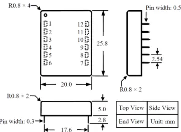
OUTLINE DIMENSIONS
The driver comes in only one package: through hole mount. It is often called DIP (Dual Inline Package) or D (short for DIP) package. And the part number is: ATLS6A201D. Dimensions of the DIP package driver are shown in Figure 9.
Figure 9. Dimensions of the DIP Package Driver Figure 10 shows the foot-print which is seen from the end side of the PCB.
Figure 10. End View of the PCB Foot-print
Figure 11 shows the foot-print which is seen from the top side of the PCB, therefore, it is a “see through” view.
“Tent” (i.e. cover the entire via by the solder mask layer) all the vias under the driver, otherwise, the vias can be shorted by the bottom plate of the driver which is internally connected the ground.
See Figure 11 and 12, it is recommended to use large copper fills for VPS, LDC, and the LDA pins, and other pins if possible, to decrease the thermal resistance between the module and the supporting PCB, to lower the module temperature.
Figure 11. Top View of the Top Side PCB Foot-print
Figure 12. Top View of the Bottom Side PCB Foot-print Figure 12 shows the foot-print which is seen from the bottom side of the PCB.
MOUNTING
It is highly recommended to lower solder iron temperature to 310°C and solder the driver manually, so that the internal
contents of the driver would not be affected.
After the soldering, it is also safe to check the laser driver’s functionality by using the “dummy laser” before connecting a real laser diode as mentioned previously on page 5.
WARNING: This module can only be soldered manually on the board by a solder iron at < 310ºC (590ºF), it cannot go through a reflow oven process.
NOTE:The power supply may have overshoot, when happens, it may exceed the maximum allowed input voltage, 6V, of the controller and damage the controller permanently. To avoid this from happening, do the following: 1. Connect the controller solid well with the power supply before turning on the power.
2. Make sure that the power supply has sufficient output current. It is suggested that the power supply can supply 1.2 to 1.5 times the maximum current the controller requires.
3. When using a bench top power supply, set the current limit to >1.5 times higher than the maximum current the controller requires.
ORDERING INFORMATION
Table 3. Part Number
Part Number Description
ATLS6A201D 6A constant current driver in DIP package
ATLS6A201D-PD 6A constant current driver with a pull-down resistor of 55K to the ground in SDN pin Table 4. Unit Price
Quantity (pcs) 1 - 9 10 - 49 50 - 199 200 - 499 ‡500
ATLS6A201D
ATLS6A201D-PD $84.0 $80.0 $76.0 $72.0 $68.0
NOTICE
1. ATI warrants performance of its products for one year to the specifications applicable at the time of sale, except for those being damaged by excessive abuse. Products found not meeting the specifications within one year from the date of sale can be exchanged free of charge.
2. ATI reserves the right to make changes to its products or to discontinue any product or service without notice, and advise customers to obtain the latest version of relevant information to verify, before placing orders, that information being relied on is current and complete.
3. All products are sold subject to the terms and conditions of sale supplied at the time of order acknowledgment, including those pertaining to warranty, patent infringement, and limitation of liability. Testing and other quality control techniques are utilized to the extent ATI deems necessary to support this warranty. Specific testing of all parameters of each device is not necessarily performed, except those mandated by government requirements.
4. Customers are responsible for their applications using ATI components. In order to minimize risks associated with the customers’ applications, adequate design and operating safeguards must be provided by the customers to minimize inherent or procedural hazards. ATI assumes no liability for applications assistance or customer product design.
5. ATI does not warrant or represent that any license, either express or implied, is granted under any patent right, copyright, mask work right, or other intellectual property right of ATI covering or relating to any combination, machine, or process in which such products or services might be or are used. ATI’s publication of information regarding any third party’s products or services does not constitute ATI’s approval, warranty or endorsement thereof.
6. IP (Intellectual Property) Ownership: ATI retains the ownership of full rights for special technologies and/or techniques embedded in its products, the designs for mechanics, optics, plus all modifications, improvements, and inventions made by ATI for its products and/or projects.