Using Coupled Lines to Produce Highly Efficient Square
Pulses for VF-TLP
Timothy J. Maloney and Steven S. Poon
Intel Corporation, 2200 Mission College Blvd., Santa Clara, CA 95052 USA tel.: 408-765-9389, e-mail: [email protected]
Abstract - A directional coupler can produce a z-matched square pulse, if a voltage step with overshoot of the
correct magnitude and timing is used. Using an augmented transmission line to produce the overshoot, and strong coupling in the coupler, square pulses with high volts per charging volt and high return loss are demonstrated.
I. Introduction
Short pulses at high current can be generated by charging a transmission line and using the (typically) 50-ohm impedance and high breakdown voltage of the transmission line to generate the high current for a short time [1]. The polarized matched load as described in [1] is adequate termination for the far end of the line for pulses of about 50 nanoseconds and longer, as long as the target device impedance is 50 ohms or less, but because diode turn-on time becomes an issue, for shorter pulses it is best to use a charged line with an attenuator as shown in Figure 1 [2]. This does not provide a perfectly impedance-matched (or z-matched) source, but if the attenuator used is –X dB, then the reflected pulses from the target will produce an echo that is down by 2X dB from the original pulse. For the interest in pulses resembling electrostatic discharge (ESD) as in [2], some pulses are very short, less than 10 nanoseconds (nsec). In the case of charged device model (CDM) ESD, this is the time scale of the event and the length of pulse one would want, maybe 2-3 nsec or less. It is customary to choose an attenuator –X of at least 6 to 10 dB so that any “echo” pulses from an unmatched Zdut and the open end of the charged line (Rhv is megohms) are at least 12 to 20 dB, respectively, down from the main pulse. This reduces the strength of the ultimate achievable pulse, of course, usually limited by the maximum voltage the switch S1 can tolerate. It would be that voltage reduced by X dB that would describe the maximum short pulse that this conventional technique can achieve. For example, there are plenty of high-speed mercury-wetted coaxial relays that can be used for S1 in a 50-ohm
environment, but most are limited to about 1-1.5kV. Relays suitable for S1 get more and more expensive as voltage tolerance goes up but there are very few that work above 3kV and still produce a stable, reproducible high-voltage arc. Recalling that a charged 50 ohm line switched into a matched 50 ohm load will suffer a 2x voltage drop just because of the 50 ohm source impedance, adding a 10 dB attenuator (3.16x) then reduces the resultant voltage into a 50 ohm load to less than 500V. This is still approaching 10 amps peak current, but for simulating destructive CDM ESD we would like to achieve more than that, and perhaps put less engineering into the switch. The length of the pulse depends on the electrical length of the main transmission line to the left of S1 in Fig. 1, often 3 nsec per foot (30 cm) of cable length. It will be something in that range depending on exact signal propagation speed, which depends on the dielectric constant of the cable insulator, and depends on the round-trip time for the signal through the cable. Signal detection, on the right of Fig. 1, is done with a high impedance scope interface, e.g., a resistive pickoff tee.
Figure 1. Traditional transmission line pulse (TLP) technique for short z-matched pulses, adapted from [2].
II. Coupled line pulse methods
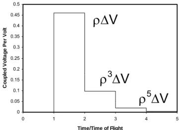
Use of a quarter-wave, two-line directional coupler to produce short, CDM-like pulses from an impedance-matched source was filed as a patent and then discussed by these authors at this conference in 2004 [3, 4]. However, the closest that one can come to square pulses, as preferred for VF-TLP, is to have a fast rise time (as compared with transit time of the coupler) and a stair-step series of pulses as shown in Figure 2. Since this series goes as odd powers of ρ (ρ
the coupler reflection coefficient) [5], the tailing pulses strengthen with coupler strength. Yet strong coupling produces the strong pulses that we like, so there is considerable incentive to modify the system of [4] to produce square pulses.
The mathematics of the high-voltage pulse-forming technique, including the series in odd powers of ρ, is derived in [4] and [5]. Now we’d like to eliminate the trailing series of echo pulses, leaving the initial square pulse. We claim that if the step function input to the coupler is altered so that a brief overshoot occurs, with a step down in voltage after one time step (round trip time of flight of the coupled line section), the voltage in the succeeding time steps can be canceled out. This is seen in Figure 3, the response to an abrupt step. It is clear that a step down of ρ2V, after
one time step, produces its own negative voltage series over an infinite number of time steps, but it cancels out the rest of the positive voltage series produced by the initial step. The coupler response will of course be a single square pulse, lasting a single
time step. Rise and fall times of the voltage are presumed to be short compared with the electrical length of the coupler.
0 0.05 0.1 0.15 0.2 0.25 0.3 0.35 0.4 0.45 0.5
0 1 2 3 4 5
Time/Time of Flight
C
o
u
p
le
d
Vo
lt
a
g
e
Pe
r Vo
lt
Figure 2. Ideal step response, on the coupled port, of a 2.4 dB (k=0.756) directional coupler, to an abrupt 1V traveling wave step
on the input port. One time step is 2t0 or the round-trip transit
time of the coupler. The pulse strength goes in time steps as odd powers of ρ, where and k is the coupling
constant [3-5].
It is possible to use the overshoot principle illustrated in Fig. 3 to modify the pulsing scheme of [4] so that the trailing voltage series is canceled and a single pulse results [6]. This is done by adding a special open stub, including a resistor, at the front end of the charged line as shown in Figure 4. The electrical length of the stub transmission line matches that of the
R
V
Z
DUT
????
Zo
= 50
-dB
S1
R
HV
V
HV
Z
DUT
Z
o
= 50
Ω
????
Attenuator
TLP SQUARE PULSE
GENERATOR
Ω
-XdB
S1
to scope
(hi-Z)
ρ∆
V
ρ
3∆
V
ρ
5∆
V
2
1
1 k
k =
ρ
coupler. The idea is to lower the driving line impedance momentarily so that the desired overshoot is achieved. The overshoot comes to an end after the wave propagating into the stub reflects off the open end and heads back to the junction, whereupon the resistor and the main line impedances (e.g., 50 ohms each way) fairly well match the stub impedance.
Figure 3. Modified step function with overshoot lasting one time step of the coupled lines. Appropriate matched coupled lines will respond to this function with a single coupled pulse of magnitude
ρV, lasting a single time step.
Other possibilities for the overshoot pulse and prolonged following pulse are possible, of course, such as the “coaxial double pulse” method described at the 1999 EOS/ESD Symposium [7]. Evaluating whether that or other methods offer any advantage over what is described here is beyond the scope of this paper.
III. Design Equations
The pulse system of Fig. 4 produces a two-part step function as in Fig. 3. The general expressions for the equivalent output impedances of the charged lines, and the voltage division relations, are useful for describing the capabilities of the pulser.
The initial low-Z output impedance Z1 for the
overshoot portion of the pulse is the parallel combination of the charge line and the stub, plus the switch resistance, all as labeled in Fig. 4:
Rsw
Zs
Rs
Zx
Zs
Rs
Zx
Z
+
+
+
+
=
(
)
1
.
(1)As discussed above, the impedance-matching condition for the stub into the line and coupler is
,
Zx Z
Zx Z Rs Zs
L L
+ +
=
where Z
L=Z
c+Rsw.
(2)Once the stub has emptied out, the pulse output impedance Z2 rises so that the voltage drops for the
rest of the pulse as in Fig. 3:
.
2 Zx Rsw
Z = + (3)
Now the pulse magnitudes come out from the voltage divider relation with the coupler having system impedance Zc, according to
,
1
Z
Zc
Zc
Vch
Vhi
+
=
and
.
2
Z
Zc
Zc
Vch
Vlo
+
=
Figure 4. Pulse system of [3,4] with resistor and open stub added as shown, to produce overshoot. For a 50 ohm (=Zx=Zc) main line, Rsw=0, and 1.9 dB (k=0.8) coupler, stub Rs=12.5 ohms and line impedance Zs=37.5 ohms works well and results in a short, square coupled pulse. Coupler is matched at through and isolated ports.
}
ρ
2V
V
Coupled
Thru L
Vch 10 Meg
Iso Coupler
Zc In
Device
R-C termination for slow ending pulse Charged coaxial cable, Zx
Zx
Zs
Rs
The condition for the step height
1
−
=
ρ
2Vhi
Vlo
(Fig.
3 and discussion above) is thus solved by
.
1 2
2
1 =
ρ
+ + − Z Zc Z Zc (4)
These four numbered equations describe the possible situations for which a stub pulser will produce a single square pulse, as desired. The time delay of the stub is presumed to be matched to the coupler time delay.
The theoretical limit of the Fig. 4 scheme is reached when Rs=0, which happens at fairly strong coupling. For the ideal case of Rsw=0 and Zx=Zc, this is at
ρ=√3/3, or 0.577…, at which point k=√3/2, or 0.866…, meaning that a 1.25 dB coupler would need to be used.
The ideal stub impedance Zs and matching resistance Rs are functions of the coupling constant and the other impedances. Using equations (1) to (4), and with zero switch resistance Rsw and Zc = Zx, Zs can be calculated as
⎟⎟ ⎠ ⎞ ⎜⎜ ⎝ ⎛ −
= 1 1
4
ρ
2c s
Z
Z (5).
So for the case of Zc=Zx=50 ohms and no switch resistance, Zs is 25 ohms or above.
The common situation is for Zc and Zx to be equal, and chosen to be a familiar value of system impedance in manufacturing, like 50 ohms. However, note that there is nothing about the design in Fig. 4 that cannot be captured on a single PC board of reasonable size. The coupler can be designed in stripline, as can the matching stub with a chip resistor. The “long” line Zx need only be long enough to be terminated as shown by a large capacitor C and matching resistor Zx so that a “long” pulse is produced.
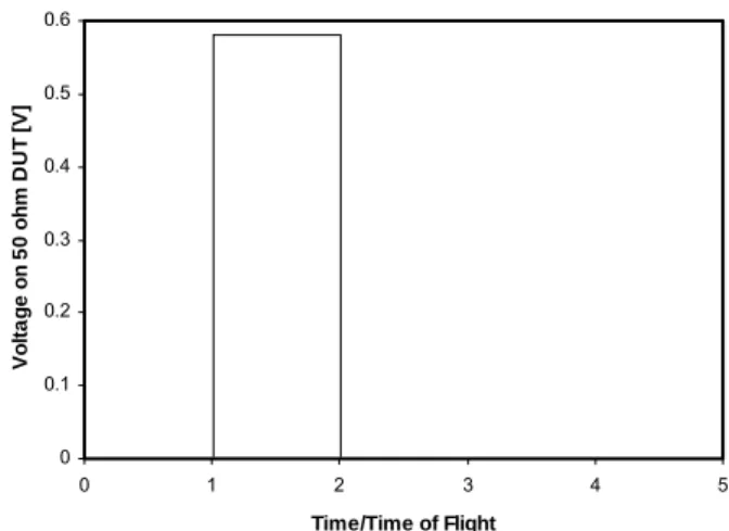
As a check on the basic stub pulser theory, coupled line simulations of the complete setup of Fig. 4 confirm that a single square pulse is generated by the stub pulser, as shown in Fig. 5.
Although the overshoot produced by the stub is capable of suppressing echo pulses when the load is matched to the system, the cancellation will not be perfect if there is a mismatch. In practice, a device with good ESD protection is likely to have low resistance compared to the system impedance. Figure 6 shows the typical current pulses through the device under test when the load is a short to ground.
0 0.1 0.2 0.3 0.4 0.5 0.6
0 1 2 3 4 5
Time/Time of Flight
V o lt ag e o n 50 o h m DU T [ V ]
Figure 5. Simulated coupled response for system of Fig. 4 with 2.4 dB coupler. Pulse is 4.71 dB down from step voltage, or 0.58 volts per traveling wave volt. The second and succeeding time step pulses (Fig. 2) are eliminated, down 112 dB in this simulation. -4 -2 0 2 4 6 8 10 12 14
0.0E+00 2.0E-09 4.0E-09 6.0E-09 8.0E-09 1.0E-08
Time [s] C u rr e n t t h rough S hort [ m A ]
Attenuator Stub Pulser
Figure 6. Current pulses generated by TLP systems when the device under test is a short. The stub pulser used for the simulation has a 1.9 dB coupler, 10 Ω switch resistance, and 1 V charging voltage, and is compared to a 6 dB attenuator system.
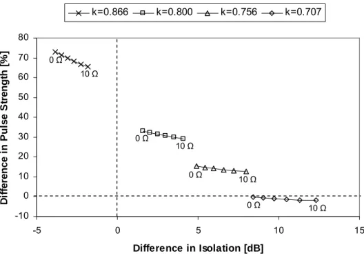
Note that the stub is no longer able to suppress echo pulses completely. Nonetheless the coupled line TLP system is still able to produce pulses with higher amplitude and lower echoes than the traditional (6 dB) system. It is possible to trade off improvements in pulse amplitude to improvements in echo pulse reduction by varying the coupling constant of the directional coupler. Higher pulse amplitude will result with higher coupling, but the echo pulses will become larger.
-10 0 10 20 30 40 50 60 70 80
-5 0 5 10 15
Difference in Isolation [dB]
D
iffe
re
n
c
e i
n
P
u
ls
e
S
tr
e
n
g
th
[%
]
k=0.866 k=0.800 k=0.756 k=0.707
0 Ω
10 Ω
0 Ω 10 Ω
0 Ω
10 Ω
0 Ω 10 Ω
Figure 7. Simulation results showing improvement of pulses generated by stub pulser versus traditional 6 dB attenuator TLP, and how pulse amplitude and isolation trade off. Data for each value of k is collected with different switch resistances ranging from 0 to 10
ohms.
As can be seen from the graph, the design space can span from equal pulse strength with smaller echo pulses (~8 dB more isolation) to equal isolation with higher pulse strength (~73% difference), and can be tuned by changing the coupling constant. Also shown are the effects of the switch resistance. Increased switch resistance tends to reduce the pulse strength advantage slightly, but causes substantial gains in the isolation. Please note that when adding switch resistance to the model, we did not optimize every design feature of both schemes. But we became convinced that doing so would change the results of Fig. 7 very little. Another advantage of the stub pulser with finite switch resistance is that pulse fall time is very likely improved over the attenuator method, as the latter suffers a mismatch with Rsw that lengthens the pulse fall time, unless the attenuator is completely redesigned to capture the Rsw, and of course Rsw can vary with voltage.
When considering Fig. 7, it is useful to review the baseline amplitude (i.e., pulse efficiency) and isolation data upon which the “difference” results are based. At Rsw=0, the 6 dB attenuator method has a 0.25V/volt pulse efficiency (0.25 volt per volt of charge on the Zx line) and the stub pulser ranges up to 0.433V/volt, some 73% higher. The 6 dB
method always has 12 dB of isolation at Rsw=0, due to the round trip through the attenuator. Fig. 7 thus shows relative improvement of the stub pulser.
IV. Experimental Results
The scheme of Fig. 4 was implemented for a 5 nanosecond pulser and a 1.9 dB coupler, the same kind of coaxial line coupler used in [3,4]. For the Rs and Zs shown in the Fig. 4 caption, note that the 25 ohm (2-way) line impedance and 12.5 ohm resistance match the 37.5 ohm stub (the stub is easily realized with two parallel 75 ohm cables). Also, the stub and R result in an additional 50 ohm line feeding the pulse at the outset, with the result that the initial impedance is 25 ohms. After the stub boost is over, the voltage goes from V to 0.75 V (i.e., 2/3 charging voltage to half), as the rest of the 50 ohm line follows. Following Fig. 3, this is consistent with ρ=0.5 or k=0.8, very close to the conditions of our coaxial coupler in [3-4].
theoretical 33.3% efficiency because of arc resistance in the switch (Rsw), a limitation of any TLP setup. However, efficiency is much higher than the 22% or so that we achieve with a pulser made with a short line and a 6 dB attenuator. Fig. 7 shows that this is consistent with Rsw of about 10 ohms.
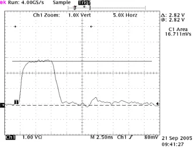
Figure 8. Stub-boosted coupled 5 nsec pulse observed through 50X attenuator. Conditions as in Fig. 4, 500V charge on line.
V. Discussion
We now discuss a few refinements to the stub pulser that may prove to be useful in later implementations.
Another embodiment of the resistive stub of Fig. 4 is shown in Fig. 9. With a “loop stub” like this, one can achieve performance equivalent to the simple R-Z stub of Fig. 4, yet possibly with more readily available transmission lines (100 ohm twisted pairs, in the example of Fig. 9). The waves on the stub propagate back through the loop, through each other to the other side and are fairly well z-matched by the series resistor and the 50-ohm main lines. Figure 7 suggests a likely use of of the stub pulser over the attenuator method in the range of ordinary “3 dB” couplers, where that term usually means 3 dB or better coupling over an octave. This means 2.4 dB at mid-band, or k=0.756. The echo pulse, which is balanced around zero, at these levels of coupling is still sufficiently weak, as Fig. 7 indicates. Fig. 6 shows that even stronger couplers are fairly good on isolation. However, as one looks to scale up the strength of pulses even further by using even stronger couplers, perhaps to the theoretical limit of ρ=0.577 and with the stub boost,
one reaches 0.433 V/volt of the line charge voltage, or a 73% improvement over the best 6 dB attenuator pulse (0.25V/volt), as noted earlier. But Fig. 7 suggests that isolating out the echo pulse is called for. One looks for a way to have the stub turned on for its voltage-generating function but then turn off in time for the reflected pulse from the device. With the electrical length to the device under test limited only by dispersion (i.e., quality of the transmission lines), it is clear that we have multiple nanoseconds to accomplish this task.
Figure 9. Loop stub, also providing overshoot pulse for 50 ohm transmission line step generator. Typical values of R and Z are given and would match to a coupler in the range of 3 dB with half the electrical length of the loop.
Consider realizing the resistive section of an R-Z stub with a high-voltage power MOSFET in the ON condition, as shown in Fig. 10. As long as the breakdown voltage after turnoff is high enough to stand off the echo pulse, the FET will isolate the rest of the stub from the echo pulse and thus preserve the z-matched source of Fig. 4.
Figure 10. R-Z stub with gated hi-voltage MOSFET as resistive element.
R=75 R
Z=100
=75
R=50
R=50
Note that the size of the MOSFET need not be very large in order to have an ON resistance, with reasonable gate voltage, of the (at least) several ohms expected for these kind of R-Z stubs. The small size allows low source-drain capacitance, and therefore weak coupling of the echo pulse to the rest of the stub, as desired. The prospects for power FET cells with high breakdown voltage and high conductance per unit width of gate are good, as SiC FETs are being developed that break all previous records [8] and indicate that MOSFETs suitable for the function of Fig. 10 are improving all the time. Even a present-day silicon MOSFET realization for Fig. 10 might be possible. A circuit suitable for triggering the OFF gate voltage of the FET in Fig. 10, once the step is generated, can be developed with standard methods.
VI. Conclusions
The high-voltage pulse-forming technique described earlier [3-5] is supplemented in order to enable production of impedance-matched high-voltage square pulses. This is done by means of a resistive stub, tuned to the coupler being used, producing an overshoot in the step function driving the coupler. These short, square pulses are needed for many studies of IC components related to ESD, particularly relating to the charged device model (CDM). The new method allows at least 15-35% more voltage over the attenuator method for generating short square pulses. The new method also increases isolation, i.e., reduces the undesired echo pulse produced by an unmatched load (device under test) and allows that feature to be traded off against amplitude gain. If an active high-voltage MOSFET is used for the resistive part of the stub, the undesired echo pulse can nearly vanish and also should allow up to 60-70% voltage improvement over the attenuator method.
Acknowledgements
The authors wish to thank Tina Cantarero for the hardware construction and for many of the lab
measurements. We also thank Jose Maiz, Mohsen Alavi and Babak Sabi for managerial support, and John Benham for manuscript review.
References
[1] T. Maloney and N. Khurana, "Transmission Line Pulsing Techniques for Circuit Modeling of ESD Phenomena", EOS/ESD Symposium Proceedings, 1985, pp. 49-54.
[2] ANSI/ESD SP5.5.1-2004: “Electrostatic Discharge Sensitivity Testing Transmission Line Pulse (TLP) Component Level”, draft standard practice, available from ESD Association, Inc., www.esda.org.
[3] T.J. Maloney, "Pulse Coupling Apparatus, Systems, and Methods", US Patent Application, filed by Intel June 26, 2003.
[4] T.J. Maloney and S.S. Poon, “Using Coupled Transmission Lines to Generate Impedance-Matched Pulses Resembling Charged Device Model ESD”, 2004 EOS/ESD Symposium Proceedings, pp. 308-315.
[5] T.J. Maloney and S.S. Poon, “Total Charge Theorem for Directional Couplers and Z-matched Coupled Lines”, IEEE Microwave and Wireless Components Letters 18, pp. 413-415, June 2005.
[6] T.J. Maloney and S.S. Poon, "Pulse Transport Apparatus, Systems, and Methods", US Patent Application, filed March 31, 2005.
[7] M. Kelly, L.G. Henry, J. Barth, et al., ”Developing a Transient Induced Latch-up Standard for Testing Integrated Circuits”, 1999 EOS/ESD Symposium, pp. 178-189.
![Figure 4. Pulse system of [3,4] with resistor and open stub added as shown, to produce overshoot](https://thumb-us.123doks.com/thumbv2/123dok_us/8195146.2172533/3.918.106.636.655.1102/figure-pulse-resistor-open-added-shown-produce-overshoot.webp)