G.Mahalakshmi, P.Sathish kumar IJSRE Volume 05 Issue 04 April 2017 Page 6364
Volume||5||Issue||04||April-2017||Pages-6364-6373||ISSN(e):2321-7545 Website: http://ijsae.in
Index Copernicus Value- 56.65 DOI: http://dx.doi.org/10.18535/ijsre/v5i04.09
Design of Solar PV Fed OP-AMP Inverter For Domestic Purposes
Authors
G.Mahalakshmi1, P.Sathish kumar2
Department of Electrical & Electronics Engineering,Sri Krishna College of Engineering &Technology,Coimbatore, India,
E-mail: [email protected] [email protected]
ABSTRACT
This paper deals with the design of solar powered standalone op-amp inverter which converts the variable DC output of a photovoltaic solar panel into AC that can be fed toloads. The area’s where the electrical grid connectivity is not possible on those area they can install the solar PV panel for electricity. Photovoltaic inverter system would make life much simpler and more convenient. This Inverter act as a backup power during outages, battery charging or for typical household applications. The system converts verylow DC voltage with highly variable power from the solar panel to the AC output voltage of 230V/50Hz sinusoidal output. By using op-amp as inverter, the cost of the system, sizeis reduced. It is more flexible to the required output voltage level without reducing the efficiency of the circuit. The overall objective is to design thesystem with minimum cost and minimum Total Harmonics Distortion in the output ac sine wave with the help of Op Amp inverter and transistor multivibrator. Herethe multivibrator will give gate signal to the MOSFET switches. MATLAB Simulations are done and the results were shown. The THD of the Inverter is reduced to 1.6% and the cost of the inverter Inverter also reduced.
Keywords- Total Harmonics Distortion, OP-AMP inverter, Transistor Multivibrator, MOSFET,Solar PV panel.
1.INTRODUCTION
G.Mahalakshmi, P.Sathish kumar IJSRE Volume 05 Issue 04 April 2017 Page 6365
2.BLOCK DIAGRAM OF PROPOSED WORK:
Fig.1 Block Diagram
Fig 1 shows the block diagram of the proposed work. Solar PV cell converts the sunlight irradiation energy into electrical energy. Due to variation the irradiation level the output various from the minimum voltage to its maximum output voltage. We won’t get the constant output voltage at all time. In order to make it as a constant voltage. We need to provide the voltage regulator which will produce the constant output of 10V for a variable input of (3.2V – 20V) range. The regulated output voltage is used to charge the battery From that battery the supply is given to the another voltage regulator for a constant output voltage at any time, in order to prevent the voltage drop due to the discharge of battery. From the battery to the inverter circuits this regulated voltage is supplied to multivibrator and MOSFET switches. Multivibrator produces a square pulse of 50HZ at both transistors of multivibrator. The pulse are out of phase with each other and it is applied to the MOSFET as a gate signal. When the pulse is high MOSFET is ON, when the pulse is low MOSFET is OFF, when MOSFET 1 is on, MOSFET 2 will be off state. When MOSFET 1 is off, MOSFET 2 will be on state
Ton = 0.01s Toff = 0.01s T = Ton + Toff T =0.02s
f = 1/0.02 = 50HZ
The drain terminals of MOSFET is connected to inverting terminal of op-amp. when the MOSFET 1 is ON “+10volt” will be applied to this op-amp in the inverting terminal. It will produces a output of 180 phase shift (-10V) with an amplification of A=-Rf/Rin. The drain terminals of MOSFET 2 is connected to non inverting terminal of the amp when those MOSFET is ON , “+10Volt” voltage will be applied to the op-amp. It will produces an output of 0 phase shift with an amplification of A=1+Rf/Rin. The summing op-amp adds the output voltage both the op-amps and finally produces the output voltage of 2 step AC square wave which is feed to the filter (LC) to make it as a sine wave of lower harmonics distortion
2.1 Block Diagram Description:
G.Mahalakshmi, P.Sathish kumar IJSRE Volume 05 Issue 04 April 2017 Page 6366
op amp will produce an output voltage of -23V. When M2 is on the inverting op amp will produce an output voltage of +23V.When the MOSFET’s (M1&M2) is in off state the output of both OP-AMP will be 0V.The output of both the AMP(inverting (-23V)and non inverting(23V))is fed to the summing OP-AMP it will add both the values and produces an output Voltage of 230Vrms,50Hz square wave.This square ac is fed to the LC filter of inductance 200mH and 80F capacitor .Finally an output of 230Volt AC sine wave of 50Hz is obtained
3. SIMULATION OF PROPOSED WORK:
Design of Op-amp Inverter is Simulated using MATLAB Software and the results of Simulation of Voltage regulator ,Multivibrator, Inverting and Non-Inverting Amplifier ,Summing Amplifier output was shown stage by stage in the consecutive chapters.
3.1 Simulation of Voltage Regulator Circuit :
Here the figure.2 indicates that the fluctuating DC output voltage of solar panel is made as supply to the voltage regulator . The zener diode maintains the non-inverting terminal input of the op-amp to 3.2V, and then the op-amp has a large gain, the op-amp inverting input and output are at the same voltage 3.2V. Hence the regulator voltage output is 3.2*(R2+R3)/R3. The NPN bipolar transistor connected to OP-Amp and input supply is to provide higher current .
Capacitor1=1microFarad,R1=4.7Kohm,R2=1Kohm,R3=470ohm.
Fig.2 Voltage Regulator Simulation Circuit
3.2 Voltage Regulator Simulation Circuit Output:
Time(s)
G.Mahalakshmi, P.Sathish kumar IJSRE Volume 05 Issue 04 April 2017 Page 6367
Figure.3 shows the regulated output voltage of 10V from the voltage regulator for a varying supply voltage of 3.2V to 20V from the solar PV panel. This Output voltage is given to the battery for charging purposes and connected to an Voltage regulator2 for constant voltage discharge of battery though an coupling capacitor of 1micro Farad.
Fig.4 Battery and Voltage regulator2
In this Figure 4. capacitor2 is a DC coupling capacitor of 1microFarad. The output of Voltage regulator 2 is fed to Multivibrator and MOSFET M1 and M2 of Non-inverting and Inverting OP-Amp respectively.
3.3 Simulation Of Multivibrator Simulation Circuit :
An AstableMultivibrator is the multivibrator which has no stable states. Its output voltage oscillates continuously between a two unstable states 0V&10V without any external triggering circuits. The time period of each states are determined by the time constant (RC) where R is resistor and C is capacitor.
Astable Multivibrator using Transistors – Circuit
Fig.5 AstableMultivibrator Simulation Circuit R1=16.7Kohm,R2=16.7Kohm,C1=0.9microF,C2=0.9microFarad,R=500ohm Here diode1 and diode2 is used to get the output waveform with sharp edges.
In the Figure.5 shows circuit of transistor multivibrator, we can find two transistors which is wired as a switch. When a transistor is in ON state, its collector and emitter terminals are short circuited. But when it is in OFF state, its collector and emitter terminals are open circuited. So in the above multivibrator circuit when a transistor is in OFF state its collector voltage is equal to Vcc(10V) and when it is in ON state its collector will be grounded(0V). When one transistor is in ON state and the other is in OFF state. The OFF time of transistor is determined by RC time constant.
G.Mahalakshmi, P.Sathish kumar IJSRE Volume 05 Issue 04 April 2017 Page 6368
3.4 Working:
When the circuit is switched on one transistor will driven to saturation region(ON) and other will driven to cutoff region(OFF). Consider TR1 is ON and TR2 is OFF. During the Capacitor C1 is charging to Vcc through 500ohm resistors(R) the transistor TR1 is ON and the TR2 is OFF due to the negative voltage from the discharging capacitor C2 . So the ON time of transistorTR2 is determined by R1C2 time constant. After a R1C2the capacitor C1 discharges completely and starts charging in opposite direction through resistor R1.When the Capacitor C2 charges to a voltage of 0.7V the transistor TR2 turns ON and capacitor C1 starts discharging. The negative voltage from the capacitor C1 .Which makes the Transistor TR1 to turns offand the capacitor C2 starts charging toVcc through resistor R. Then the transistor TR2 remains in ON state. In the next cycle the above process takes place in opposite direction i.e C2 discharge and C1 charge. Transistor TR1 ON and TR2 OFF .
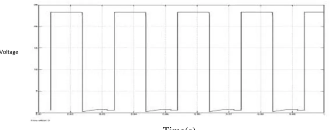
3.5 Multivibrator Output Waveform:
Time(s)
Fig.6 Multivibrator output wave form
In the Figure.6 shows the output wave form of astablemultivibrator from TR1 and TR2 ON time = 0.01s; OFF time = 0.01s; Total time=0.02s(50Hz) [For both the output signal ]
4. SIMULATION OF NON- INVERTING OP-AMP CIRCUIT:
When the MOSFET is in on state Non- Inverting OP-Amp Circuit produces a output voltage of 23Volts.Where the input is 10V . Figure.7 shows the simulation circuit of Non-Inverting OP-Amp Circuit . Drain of MOSFET is connected to Non-Inverting terminal of OP-Amp. Source of MOSFET is connected to the output of voltage regulator2.Gate is connected to the output of Multivibrator transistor TR1.
In this Figure 7.The value of resistance in this non-inverting OP-Amp simulation circuit: R11=1.3Kohm,R12=1Kohm.
Fig.7 Non- Inverting OP-Amp Circuit:
G.Mahalakshmi, P.Sathish kumar IJSRE Volume 05 Issue 04 April 2017 Page 6369
4.1 Non- Inverting Op-Amp Output Waveform:
Time(s) Fig 8.Non- Inverting OP-Amp output waveform:
In figure 8 shows the output of Non inverting OP-Amp. It produces a positive voltage of 23 Volts. For 0.01s it produces +23V and next 0.01s it produces 0V alternatively.
4.2 SIMULATION OF INVERTING OP-AMP CIRCUIT:
When the MOSFET is in on state Inverting OP-Amp Circuit produces a output voltage of -23volts.Where the input is 10V. Inverting OP-Amp always produces the output voltage with a phase difference of 180 degree with the input supply voltage. Figure.9 shows the simulation circuit of Inverting OP-Amp. Drain of MOSFET is connected to Inverting terminal of OP-Amp. Sources of the MOSFET is connected to the voltage regulator 2 output .Gate is connected to the multivibrator TR2 transistor output.
In this Figure 9.The value of resistance in this inverting OP-Amp simulation circuit: R11=1.7Kohm,R12=4.81Kohm.
Fig 9. Inverting OP-Amp Simulation Circuit:
4.3 Inverting Op-Amp Output Waveform:
Time(s)
Fig.10 Inverting OP-Amp output waveform Voltage
G.Mahalakshmi, P.Sathish kumar IJSRE Volume 05 Issue 04 April 2017 Page 6370
In figure 10 shows the output of inverting OP-Amp. It produces a Negative voltage of 23 Volts For 0.01s it produces -23V and next 0.01s it produces 0V alternatively.
4.4 Simulation of Summing OP-AMP Circuit:
Summing OP-AMP add the output signal both inverting and non-inverting op amp and produce an output signal of 230Vrms square ac signal. Figure.11 shows the simulation circuit of Summing OP-Amp. The output voltage of non-inverting Amp is given to R11 resistor and the output voltage of inverting Op-Amp is given to R12 resistor. . . .
.. …………... ………..
Fig 11. Summing OP-Amp simulation circuit In this figure 10 the value of resistance is R11= 700ohm,R12=700ohm.
The input voltages are +23V and -23V are added up and the amplified with a gain of 14 in the OP-Amp and The Output Is 330V Peak To Peak Rectangular Ac Voltage Is Produced.
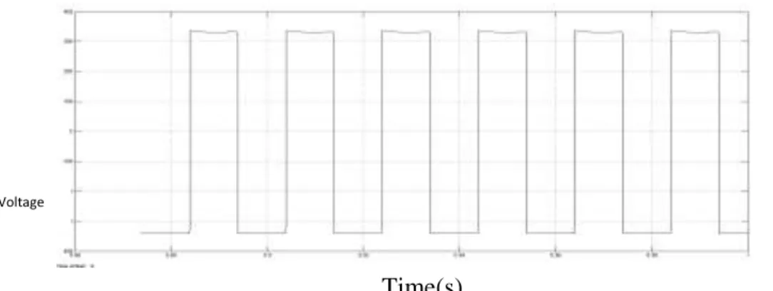
4.5 Summing OP-AMP Output Wave Form:
Time(s)
Fig.12 Summing OP-Amp output wave form
Figure.12 shows the Output Voltage waveform of summing OP-Amp. 330V Peak rectangular ac voltage with a frequency of 50Hz is produced
4.6 Simulation of LC Filter Circuit:
LC filter is used to convert the AC rectangular wave to 230Vrms AC sine wave Figure .13 shows the LC Filter circuit along with the resistive load of 200 ohm.
G.Mahalakshmi, P.Sathish kumar IJSRE Volume 05 Issue 04 April 2017 Page 6371
R=42 ohm L=220mH C=80microF
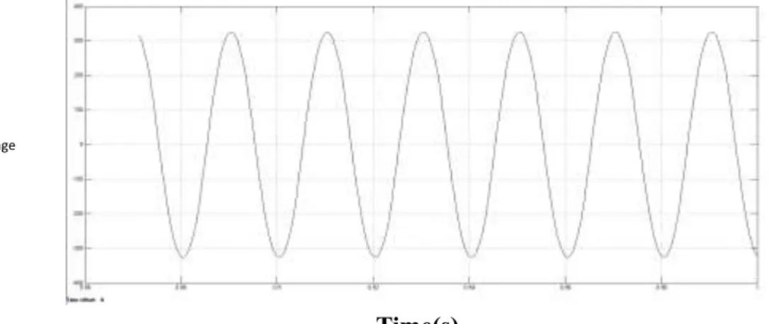
4.7 Output Wave Form:
Time(s)
Fig 14. LC filter output waveform
Figure 14. shows the output voltage waveform of LC filter Which is 330V peak Voltage and ac sinusoidal waveform at a frequency of 50 Hz.
5.SIMULATION OF OVERALL CIRCUIT CIRCUIT DIAGRAM :
Fig.15.Overall Simulation circuit
Figure 15. Gives the overall view of solar fed OP-Amp inverter circuit connections.
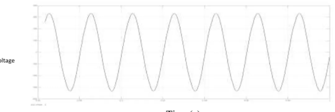
5.1 Output Wave Form With Resistive And Inductive Load Output Waveform With Resistive Load:(R=200 ohm)
VOLTAGE WAVEFORM:
Time(s)
Fig 16.Output Voltage wave form with resistive Load
Figure 16. shows the output voltage waveform of Resistive Load Which is 330V peak Voltage and ac sinusoidal waveform at a frequency of 50 Hz.
Voltage
G.Mahalakshmi, P.Sathish kumar IJSRE Volume 05 Issue 04 April 2017 Page 6372
Output Waveform With Inductive Load:(L=400mh)
VOLTAGE WAVEFORM:
Time(s)
Fig 17.Output Voltage wave form with Inductive Load
Figure 17. shows the output voltage waveform of inductive Load .Which is 330V peak Voltage and ac sinusoidal waveform at a frequency of 50 Hz.
6. THD ANALYSIS:
Total harmonic distortion play an important role in rotating machinaries if the THD is higher the loss will more in rotating machines , ununiform torque and lots of noice will be produced.Which reduces the life time of the machinaries. So the THD of the inverter system should be very low for the smooth operation of machines , better effeciency and long life time.
Fig 18.THD IEEE Standard
The above Figure 18 shows the IEEE standard for THD of various systems and Applications
Fig.19.THD Analysis
From the above figure .19 .We can say that the Total Harmonic Distortion of OP-Amp inverter is 1.62% which less than 3% .According to IEEE standard if the THD is less than 3% we can use this supply for all electrical applications[6]
G.Mahalakshmi, P.Sathish kumar IJSRE Volume 05 Issue 04 April 2017 Page 6373
7. CONCLUSION:
Thus the OP-AMP inverter requires minimum number of switches that is 2 .The losses due to switching is get reduced . The power dissipated by the OP-AMP LM324 is 150milliWatt for 100 watt output we are using 12 OP-AMP therefore total power dissipation in OP-AMP is 1.8 watt only .Therefore the losses in the OP-AMP is also very low and there is no step-up transformer is used .Finally results in increasing the efficiency of the OP-AMP inverter greater than 95%.In order to have a output power of 500 watt we can use the OPA 502 OP-AMP.Here we used only the OP-AMP as a main components in the inverter .it is only the costly item compared to other component in the inverter . However the over all cost is getting reduced when compared to other inverter types. The size and weight of the OP-AMP inverter is very low because used only the small size power electronic components. The total harmonic distortion is less than 2%, therefore we are getting pure sine wave output supply which can be used as a supply for any electrical equipment’s. No IC are used here other than OP-AMP IC for generation of switching signal to op amp .
COST COMPARISON OF 400 WATT230Volt INVERTER
For the same output power and voltage ,other type of inverters cost around 9,000 rupees. But for the proposed system cost of the components are given below
1 OP-AMP =RS: 2,100 {OPA 502}
3 OP-AMP is required one for each inverting ,non inverting , summing totally
3*2100=RS:6,300.other components will not exceed RS:200.Hence,The total cost of the proposed system is 6,500.
REFERENCES
1. Damrong AMORNDECHAPHON Automotive and Transportation Technology Development
Center(ATTDC),”High-Efficiency PWM DC-AC Inverter for Small PV Power Generation System” ,2016 International Conference on Cogeneration, Small Power Plants and District Energy (ICUE 2016) BITEC, Bang-Na, Thailand, 14-16 September 2016
2. U. D. Dwivedi, Member, IEEE and ChandrakantTiwari,”A Generalized Wavelet Modulation
Scheme for Single-Phase Inverters “2015 IEEE
3. HolgerJedtberg, Student Member, IEEE, Alberto Pigazo, Senior Member, IEEE”Analysis of the
Robustness of Transformerless PV Inverter Topologies to the Choice of Power Devices”DOI 10.1109/TPEL.2016.2612888,IEEE Transactions on Power Electronics
4. MerajHasan, JunaidMaqsood, MirzaQutabBaig, Syed Murtaza Ali Shah Bukhari, Salman
Ahmed,”Design&Implementation of Single Phase Pure Sine Wave Inverter Using Multivibrator IC”,2015 17th UKSIM-AMSS International Conference on Modelling and Simulation
5. Tony Hoevenaars, P. Eng. Kurt LeDoux, P.E. Matt Colosino,”Interpreting IEEE Std 519 and
Meeting its Harmonic Limits in VFD Applications”,May 6, 2003 IEEE.
6. M.I. Jahmeerbacus and M. Sunassee,”Evaluation of Selective Harmonic Elimination and Sinusoidal
PWM for Single-Phase DC to AC Inverters under Dead-Time Distortion “,2014 IEE.
7. NarendraKumar Dheeraj Joshi and SachinSinghal,”Design and Performance Analysis of a Single Phase PWM Inverter”,978-1-4799-6042-2 2014 IEEE
8. Neharilarbil. M,NBrahami,I.S.bouchmaha,”Design and Implementation of Single Phase Solar
Inverter based on microcontroller 16F628A”978-1-4673-6673,2015 IEEE.
9. AlirezaHarrasi, Student Member, IEEE, Ahmed F. Zobaa, Senior Member, IEEE,”A cost effective