University of Windsor University of Windsor
Scholarship at UWindsor
Scholarship at UWindsor
Electronic Theses and Dissertations Theses, Dissertations, and Major Papers
2004
A SigmaDelta modulator for digital hearing instruments using
A SigmaDelta modulator for digital hearing instruments using
0.18 mum CMOS technology.
0.18 mum CMOS technology.
Iman Yassin. TahaUniversity of Windsor
Follow this and additional works at: https://scholar.uwindsor.ca/etd
Recommended Citation Recommended Citation
Taha, Iman Yassin., "A SigmaDelta modulator for digital hearing instruments using 0.18 mum CMOS technology." (2004). Electronic Theses and Dissertations. 747.
https://scholar.uwindsor.ca/etd/747
A
Modulator for Digital Hearing Instruments
Using 0.18 jim CMOS Technology
by
Iman Yassin Taha
A Thesis
Submitted to the Facility o f Graduate Studies and Research
through Electrical and Computer Engineering in Partial
Fulfillment o f the Requirements for the Degree
o f Master o f Applied Science at the
University o f Windsor
Windsor, Ontario, Canada
2004
1 * 1
Library and Archives Canada
Published Heritage Branch
395 W ellington Street Ottawa ON K1A 0N4 Canada
Bibliotheque et Archives Canada
Direction du
Patrimoine de I'edition
395, rue W ellington Ottawa ON K1A 0N4 Canada
Your file Votre reference ISBN: 0-612-96390-X Our file Notre reference ISBN: 0-612-96390-X
The author has granted a non exclusive license allowing the Library and Archives Canada to reproduce, loan, distribute or sell copies of this thesis in microform, paper or electronic formats.
The author retains ownership of the copyright in this thesis. Neither the thesis nor substantial extracts from it may be printed or otherwise
reproduced without the author's permission.
L'auteur a accorde une licence non exclusive permettant a la
Bibliotheque et Archives Canada de reproduire, preter, distribuer ou
vendre des copies de cette these sous la forme de microfiche/film, de
reproduction sur papier ou sur format electronique.
L'auteur conserve la propriete du droit d'auteur qui protege cette these. Ni la these ni des extraits substantiels de celle-ci ne doivent etre imprimes ou aturement reproduits sans son autorisation.
In compliance with the Canadian Privacy Act some supporting forms may have been removed from this thesis.
While these forms may be included in the document page count,
their removal does not represent any loss of content from the thesis.
Conformement a la loi canadienne sur la protection de la vie privee, quelques formulaires secondaires ont ete enleves de cette these.
Abstract
This thesis develops the design methodology for a low-voltage low-power XA
Modulator, realized using a switched op-amp technique that can be used in a hearing instrument. Switched op-amp implementation allows scaling down the design to the
latest CMOS technology. A single-loop second-order XA Modulator topology is chosen. The modulator circuit features reduced complexity, area reduction and low conversion energy. The modulator has a sampling rate of 8.2 MHz with an over-sampling ratio
(OSR) of 256 to provide an audio bandwidth of 16 kHz. The modulator is implemented in a 0.18 pm digital CMOS technology with metal-to-metal sandwich structure capacitors. The modulator operates with a supply voltage of 1.8 V. The active area is 0.403 mm . The modulator achieves a 98 dB signal-to-noise-and-distortion ratio (SNDR) and a 100 dB dynamic range (DR) at a Nyquist conversion rate of 32 kHz and consumes
1321 pW with a joule/conversion figure of merit equal to 161xl0’12 J/s.
Acknowledgments
First and foremost, I would like to express my sincere gratitude first to my supervisor, Professor William Miller, for giving me the opportunity to research in the field o f mixed-signal design and for his patience, guidance, constant encouragement,
technical and financial support throughout the course of the research.
I would like to express my deepest gratitude to Dr. Majid Ahmadi for his continuous encouragement and support in facing all the obstacles that affect my career.
I would like to express my best regards to Dr. Edwin Tam, of the Civil and Environmental Engineering Department, for his valuable comments.
I would like to thank Till Kuendiger for his assistant in helping me to solve the
problems in using the Cadence design tool.
Contents
Abstract... iii
Acknowledgement...iv
List of Tables... ix
List of Figures... x
Abbreviations...
xiii1. Introduction
1.1. Motivation...11.2. Objective...2
1.3. Thesis Organization... 3
2. ZA Modulator Basic Concepts
2.1. Oversampling ADC... 42.2. First Order EA Modulator...7
2.2.1 Time Domain Behavior...7
2.2.2 Z-Domain Behavior... 8
2.3. Second Order EA Modulator... 9
2.4. Performance Criteria... 11
2.4.1 Signal-to-Noise Ratio (SNR)...11
2.4.2 Signal-to-Noise-and-Distortion Ratio (SNDR)...12
2.4.3 Dynamic Range (DR)...12
2.4.4 Effective Resolution (B)... 12
2.4.5 Pow er D issipation... 13
2.5. Top-Down Design Methodology Motivation...14
2.6. Switched Op-Amp EA Modulator Design Methodology... 14
3.2 Single Loop 2 A Modulators using Half Delay Integrators...19
3.3 Cascade 2A Modulators Using Half Delay Integrators...22
3.4 Multibit Topology... 24
3.5 T opology Selection... 25
3.6 2 A Modulators Non-idealities...27
3.7 Clock Jitter Model...27
3.8 Integrator Noise Model... 28
3.8.1 Switch Thermal Noise (KT/C) M o d el... 30
3.8.2 Op-Amp Noise Model... 31
3.9 Integrator Non-idealities Model...32
3.9.1 DC Gain... 32
3.9.2 Bandwidth and Slew Rate... 33
3.9.3 Saturation... 35
3.10 Capacitor Mismatching...35
3.11 Comparator... 35
3.12 Behavioral Simulation for the Ideal 2A Modulator...35
3.13 Behavioral Simulation for the Non-Ideal 2A Modulator... 39
4. Low Voltage Low Power Design Techniques
4.1 Switch Behavior... 444.2 Single Switch Behavior... 48
4.3 Existing Solutions... 50
4.4 Original SOTechnique... 51
4.5 Modified SO Technique...52
4.6 Quantization and Circuit Noise... 54
4.7 Intrinsic Constraint of Power Consumption...57
4.8 Practical Constraints of Power Consumption... 58
4.9 Suppression of Noise Generated Inside the Loop...58
4.10 System Level Power Saving...59
5.2 Switched Op-Amp Integrator... 66
5.3 Comparator... 68
5.4 Biasing Circuit...75
5.5 Half Delay Circuit... 76
5.6 Clock Generator...77
6. System Implementation
6.1. Modulator Schematic and Implementation... 796.2. Modulator Layout Methodology... 84
6.3. Floor-planning... 85
6.3.1. Power Supply Strategy... 85
6.3.2. Interface Signals Definition... 86
6.3.3. Special Design Requirements Consideration... 86
6.3.4. Size Approximation... 86
6.4. Sub-block implementation... 87
6.4.1 Component Placement... 87
6.4.2 Special Design Requirements... 87
6.4.2.1 Matching of Fully Differential Design... 87
6.4.2.2 Guard Rings... 90
6.4.2.3 Shielding... 90
6.4.2.4 Capacitor Layout... 91
6.4.2.5 Multi-finger Transistors...91
6.4.3 Component Connection... 94
6.4.4 Sub-Block Layout Verification... 94
6.5. Building and Verifying the Modulator Layout... 100
6.6. Post-Processing... 100
6.7. Generating the GDSII File... 100
7. Conclusions and Recommended Future Work
7.1 Conclusions... 105Appendix A
A .l Slew Rate Modeling... 107 A.2 PSD Plotting... 108
A.3 SNR Calculation...110 A.3.1 Extraction of a Sinusoidal Waveform from a Bitstream... I l l
References...
112List of Tables
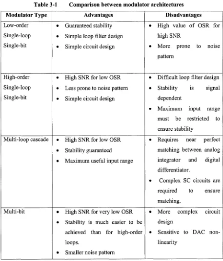
3 -1. Comparison between modulator architectures...18
3-2. Non-idealities of the fundamental basic blocks... 27
3-3. Second-order modulator coefficients and parameters... 42
3-4. Building block requirements... 42
5-1. Cell values for the op-amps... 63
5-2. Simulated performance o f the first and second op-amp... 65
5-3. Cell values of the comparator... 74
5-4. Comparator specifications... 74
5-5. Cell values for the biasing circuit... 75
6-1. Modulator specifications... 103
List of Figures
2-1. Typical ADCs block diagrams... 5
2-2. Nyquist rate and oversampling ADC...5
2-3. Pulse density output from a XA modulator for a sine wave input...6
2-4. Digital and decimation filtering in the XA ADC... 7
2-5. First-order XA m odulator...8
2-6. Z domain representation of the first-order XA modulator... 8
2-7. Second-order XA modulator... 9
2-8. Comparison of noise shaping for the first, second and third-order XA modulator...11
2-9. Oversampling ratio versus resolution for the first, second and third -order XA m odulator... 13
2-10. SO XA modulator design methodology... 16
3 -1. Classic nth order single loop XA modulator topology...19
3-2. Second-order, single-loop XA modulator topology...19
3-3. The nth order single loop XA modulator topology using half delay integrators... 20
3-4. Block diagram of a cascaded XA modulator... 23
3-5. Cascaded 2-1 XA modulator with half delay integrators...23
3 -6. Modeling a random sampling j itter... 28
3-7. Noisy integrator model...29
3-8. Single-ended SC integrator... 29
3-9. Modeling thermal noise (K T /C )... 30
3-10. Op-amp noise model...31
3-11. Real integrator model... 32
3-12. SIMULINK model for an ideal second-order XA modulator... 36
3-14. Simulated output spectra with -2 dB input sinusoidal for the
ideal second-order modulator... 38
3-15 SIMULINK model for the non-ideal second-order ZA m odulator...39
3-16 SNDR versus input amplitude... 40
3-17 Simulated output spectra with -2 dB input sinusoidal for the non-ideal second-order XAmodulator...41
4-1. Non-inverting SC integrator... 45
4-2. Complementary switch...46
4-3. Complementary switch simulation results in 0.18 pm process...47
4-4. Complementary switch with symmetrical on-resistance simulation results in 0.18 pm process... 47
4-5. Simulation results of the symmetrical on-resistance complementary switch if the minimum conductivity desired is 600 pG (equivalent to an on-resistance of 2.1KQ)...48
4-6. Simulation of the N-type switch in 0.18 pm technology...49
4-7. Simulation of the P-type switch in 0.18 pm technology... 49
4-8. The SO integrator preceded by another integrator...52
4-9. The signal swings in the modified SO technique... 53
4-10. The differential modified SO integrator cell... 53
4-11. The noise power spectral densities... 56
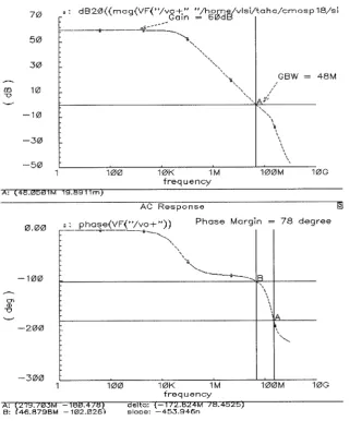
5-1. Folded cascade two stage op-amp... 62
5-2. The common-mode feed back circuit...63
5-3. The ac response of the op-amp... 64
5-4. The DC response of the op-amp... 65
5-5. SO integrator... 66
5-6. Output CM simulation result... 67
5-7. Transient response to a step input... 67
5.8. Three-stage comparator... 70
5-9. The ac response of the comparator... 71
5-10. Comparator response to a ramp input...71
5-12. Simulating hysteresis in the backward direction...72
5-13. Simulating the comparator speed... 73
5-14. Simulating the comparator propagation delay...73
5-15. The biasing Circuit... 75
5-16. Half delay circuit... 76
5-17. Half delay circuit simulation result... 76
5-18. Clock generation... 77
5-19. Timing diagram...78
6-1. Circuit schematic of the second-order single-loop XA modulator...79
6-2. Feedback network... 81
6-3. Feedback circuit implementation... 82
6-4. Second-order single-loop SO XA modulator... 83
6-5. Layout methodology... 84
6-6. Floor-planning steps... 85
6-7. Implementing the designed sub-blocks... 88
6-8. Common centroid input stage transistors...88
6-9. Op-amp layout...89
6-10. Capacitor layout with guard rings... 91
6-11. Shielding the sensitive analog signals... 92
6-12. Multi-fingering...93
6-13. Building block layout verification steps... 95
6-14. Comparator layout... 96
6-15. Clock generation layout...97
6-16. Half-delay circuit layout...98
6-17. Set-reset flip flop layout... 99
6-18. The implemented XA m odulator... 101
6-19. The generated bitstream...102
6-20. The output spectrum ... 102
Abbreviations
ADC
Analog-to-digital converterCM
Common-modeCMFB
Common-mode feedbackCMOS
Complementary metal-oxide semiconductorDAC
Digital-to-analog converterDR
Dynamic rangeDRC
Design rule checkerFF
Flip-flopFOM
Figure-of-meritGBW
Gain bandwidth productGUI
Graphical user interfaceLVS
Layout versus schematicMOSFET
Metal-oxide semiconductor field effect transistorNMOST
Negative-channel metal-oxide semiconductor transistorNTF
Noise transfer functionOp-Amp
Operational amplifierOSR
Oversampling ratioPMOST
Positive-channel metal-oxide semiconductor transistorPSD
Power spectral dnsityRMS
Root mean squareRC
Resistance capacitorSC
Switched capacitorZA
Sigma-deltaSNR
Signal to noise ratioSO
Switched op-ampSOC
System on chipSR
Slew rateSR FF
Set-reset flip-flopSTF
Signal transfer functionChapter 1
Introduction
1.1
Motivation
Modem electronics systems in computers, communications, automotive and instrumentation are mostly mixed-signal systems. An analog to digital converter (ADC) is a standard building block, unavoidable as interface between the analog world and the digital signal processing hardware. The market for portable electronic systems and system-on-chip (SOC) such as wireless communications devices and hearing aids, is
continuously expanding. Both low voltage and low power operation are of great importance for portable applications and SOC. Low voltage operation is demanded because it is desirable to use as few batteries as possible for size and weight
considerations. Low power consumption is necessary to ensure a reasonable battery lifetime.
The XA converters are based on noise shaping and over-sampling. It has been known for nearly thirty years, but only recently has the technology of high-density digital
VLSI existed to manufacture them as inexpensive integrated circuits. Without the CMOS technology, the digital filtering required in XA converters for decimation and
interpolation makes these circuits too expensive. Low voltage low power design can be
achieved as the CMOS technology is scaled down. XA converters have low sensitivity to
the component mismatches at the price of extensive use of digital processing [1],
There are a lot of architectures available to implement XA converters, from
single-loop [2] to the more sophisticated with multiple feedback loops, cascade connection or multi-bit quantization [3] [4] [5] [6] [7] [8]. Most of these architectures have been successfully implemented. CMOS XA converters with 20-bit effective resolution in instrumentation [9] [10] [11], 16-bit in audio and data acquisition [12] [13] [14] [15] [16] and 12-bit or more in communications are feasible [17] [18] [19] [20],
the inherent qualities of XA converters [22] [23] [24] [25] [26]. For digital-audio
applications, the previous researches have already proven that switched-capacitor (SC)
XA structure is a good candidate. However, these works either employ supply voltages
as high as 5 V [27], or use out-of-date CMOS technologies with bigger transistor channel
lengths [27] [28]. In the 0.18 pm technology, XA modulator is presented for digital-
audio applications using a bootstrapped switch [29]. To the author’s knowledge, there is
a lack of papers on implementation of digital-audio XA modulators with guaranteed performance that is compatible with the latest CMOS technologies. The market does post
a continuing demand to design XA modulators using technologies with channel length as
small as 0.18pm or even smaller to be compatible with the latest CMOS technologies and with less area-occupation, high-resolution, and low power.
1.2
Objectives
This thesis investigates the development o f a switched op-amp (SO) XA
modulator for digital-audio instrumentations to provide compatibility with the continuously decreasing CMOS technology feature size. The specific design objectives are:
1. To develop a top down design methodology in order to perform an analysis at the system architectural level before starting transistor level design. To use Matlab/ SIMULINK to implement the system architecture and model non-idealities.
2. To choose the proper topology to design the XA modulator for
digital-audio instrumentations, while considering low-power and low-voltage design constraints.
3. To carry out the design of the individual building blocks using the 0.18
pm CMOS process. To integrate the building blocks. To verify the designed individual circuits and the whole modulator by simulation using Hspice in the Cadence design tools.
4. To implement the Layout considering the mixed-signal design
required specifications thought post-simulation with parasitic and testing the fabricated chip.
1.3
Thesis Organization
Chapter 2 is an introduction to XA modulators. It includes discussing
oversampling ADC, analyzing the behavior of XA modulators in the Z-domain and
discussing the performance metrics. The motivation for top-down design methodology is discussed and the implemented methodology for this work is shown. In Chapter 3 different kinds of topologies are compared and the reasons for selecting the single-loop,
second-order XA modulator for this work are discussed. Non-idealities issues associated
with XA modulator design and modeling in MATLAB/ SIMULINK are given and the behavior simulation to optimize the system and building blocks parameters is then
developed. In Chapter 4, the switch design constraint and low-voltage, low-power design techniques are addressed. Chapter 5 focuses on the implementation o f each building
block in the TSMC 0.18 pm CMOS technology with the simulation results from the analog environment of the cadence design tool. Chapter 6 deals with integrating the
building blocks to implement the SO XA modulator and simulating the results. In
Chapter 2
XA Modulator Basic Concepts
This Chapter introduces the concept of oversampling ADC, describes the basic
function of the XA Modulator and explains how the XA Modulation is so beneficial for
generating high-resolution data. The performance criteria that are necessary to measure
the performance of the XA Modulator are defined. A top-down design methodology
using SIMULINK for the design of XA modulator is discussed. The motivation and the
benefits of the top-down optimization are presented, which featured a shorter design cycle, along with ease of implementation and reproducibility. The design steps for the
SO XA modulator are summarized
2.1
Oversampling ADC
Analog-to-digital converters can be separated into two categories depending on the rate of sampling. The first category samples the input at the Nyquist rate, such that:
A = 2 F
Where F is the signal bandwidth and f N is the sampling rate. The second type samples the signal at a rate much higher than the signal bandwidth. This type is called the oversampling converter [30].
$/H
<»)
Analog inpm Digitalfilter
(«?)
Figure 2-1. Typical ADCs block diagrams, (a) Nyquist rate ADC. (b) Oversampling ADC
Sampling frequency is twice the signal bandwidth.
ftvtY tvtvtr' 1"8^ /trhrhrhrh
- 2f, - f s 0 f , 2fi f(*)
2 /x - A 0 f I f , f
U T
Aliasingf
(•>)
Oversampling frequency is many times the signal bandwidth.
m
m
m-A o
fr)
Figure 2-2. Nyquist rate and oversampling ADC. (a) Frequency domain for Nyquist rate ADC. (b) Aliasing effect for Nyquist rate ADC. (c) Frequency domain for oversampling ADC.
widely spaced, as seen in Figure 2-2c. Thus using oversampling ADC, little if any, anti alias filtering is needed.
Oversampling converters typically employ SC circuit and therefore do not need sample-and-hold circuits. Quantization is provided in the form of a pulse-density modulated signal that represents the average of the input signal. The modulator is able to
construct these pulses in real time, so it is not necessary to hold the input value and perform the conversion. Figure 2-3 illustrates the output of the modulator for the positive half o f a sine wave input. For the peak o f the sine wave, most o f the pulses are high. As
the sine wave decreases in value, the pulses become distributed between high and low according to the sine wave value.
Digital signal processing should be utilized for the oversampling ADC, which
filter any out-of-band quantization noise and attenuate any spurious out-of-band signals. The output of the filter is then down sampled to the Nyquist rate so that the resulting output of the ADC is the digital data, which represents the average value of the analog voltage over the oversampling period. Figure 2-4 shows the block diagram and the frequency spectrum of the digital part.
\
“ yd(n)
*■■■■
JVC/) digital filter
n
f b f s / 1 f s
yd(f)
(bpocn
h fs
Figure 2-4. Digital and decimation filtering in the ZA ADC
2.2
First Order S A Modulator
This section examines the time domain and the frequency domain behaviour to
determine why ZA Modulation is so beneficial for generating high-resolution data. Noise shaping, which is a powerful concept used within oversampling ADC, is explained.
2.2.1 Time Domain Behaviour
A basic first order ZA modulator can be seen in Figure 2-5. An integrator and a 1-bit quantizer are in the forward path, and a 1-bit digital-to-analog (DAC) is in the feedback path of a single-feedback loop system. The 1-bit quantizer is simply a comparator that converts an analog signal into either a high or low. From the Z-domain
representation shown in Figure 2-6, the input-output relation can be written in terms of a difference equation as [31]:
y(KT) = x(KT - T ) + Qe (K T) - Qe (KT - T) (2-1)
Where K is an integer. T is the inverse of the sampling frequency ( f s). Qe is the quantization noise expressed as:
1 bit
Quantizer
Figure 2-5. First-order ZA modulator
Integrator integrator
(a) (b)
Figure 2-6. Z domain representation of the first-order ZA modulator. (a) Z-domain representation, (b) Conceptual representation.
Therefore, the output of the modulator consists of a quantized value of the input signal delayed by one sample period, plus a differencing of the quantization error between the
present and previous values. Thus, the real power of the ZA Modulator is that the
quantization noise Qe, cancels itself out to the first order.
2.2.2 Z-D om ain B ehaviour
Figure 2-6 shows the Z-domain model for the first order ZA modulator. The ideal
Z _1
modeled as a simple error source Q(Z), and the DAC is considered to be ideal. The output can be expressed as:
Y(z) = Z-1X ( Z) + ( l - z - l)Q(z) (2-2)
Where Y(z), X ( z ) and Q(z) are the z-transform of the modulator output, input, and the
quantization error respectively.
The multiplication factor of X(z) is called the signal transfer function (STF), whereas that o f Q(z) is called the noise transfer function (NTF). It can be noted that z '1 represents a unit delay, while the NTF has high pass characteristics, allowing noise suppression at low frequencies. The modulator has essentially pushed the power of the noise out of the bandwidth of the signal. This high-pass characteristic is known as noise shaping. The digital filter will then perform low pass filtering in order to remove all of the out-of-band quantization noise, which then permits the signal to be down sampled to yield the final high-resolution output
2.3
Second Order ZA modulators
Second order ZAmodulator provides a greater amount of noise shaping. A
second-order modulator is shown in Figure 2-7.
1 bit Quantizer
:(kn Delay
The output of the modulator can be expressed in the time domain as [31]:
y(KT) = x(KT - T ) + Qe (KT) - 2Qe (KT - T ) + Qe (KT - 2T) (2-3)
The output contained a delayed version of the input plus a second-order differencing of
the quantization noise Qe.
The z-domain equivalent is given by [32]:
Y(z) = z - lX ( z ) + ( l - z - l)2Qe(z) (2-4)
The NTF ( 1 - z '1) 2 has two zeros at dc, resulting in second-order noise shaping. In
general Lth-order noise shaping can be obtained by placing L integrators in the forward
path of a AS modulator. For Lth-order noise differencing, the noise transfer function
(NTF) is given by:
NTFq(z) = (1 - z ~ l)L (2-5)
In the frequency domain, the magnitude of the noise transfer function can be written as:
| NTFq ( / ) 1=11 - e jlnfr° \L = (2 sin 7fTs )L (2-6)
V olts
Second-order
Sampling frequency
Figure 2-8. Comparison of noise shaping for the first, second and third-order ZA modulator.
In practice, the single-loop modulator having noise-shaping characteristics in the form of (1-Z"')L is unstable for (L>2), unless an L-bit quantizer is used [33] [34]
2.4
Performance Criteria
The figures of merit used to characterize A£ modulator are the signal-to-noise
ratio (SNR), signal-to-noise-and-distortion ratio (SNDR), Dynamic range (DR), the effective resolution and the power dissipation.
2.4.1 Signal-to-noise ratio (SNR)
SNR is the ratio between the output power at the frequency o f a sinusoidal input and the in-band noise power. Ideally with quantization noise only, the SNR results in:
SNR(dB) = 10 log10
r A 21 2 "
V pQ J
(2-7)
2.4.2 Signal-to-noise-and-distortion ratio (SNDR)
It is the ratio o f the output signal power to the in-band noise power due to the non-idealities of the circuitry and the quantization noise. Then by definition, SNDR is given by:
SNDR(dB) = 10 log10
f A 2 12 A
\ PQ + P D J
(2-8)
Where Pd is the harmonic distortion power due to the non-idealities.
Peak SNDR is a useful metric for evaluating the capability o f a ZA modulator for
handling large in-band signals at acceptable linearity. It is especially important for applications such as digital audio applications. Peak SNDR is frequency dependant and can be used to measure the degradation of the modulator performance as the input signal increases in frequency. Since the output data is digital, discrete Fourier transform can be used to examine the data in the digital domain.
2.4.3 Dynamic range (DR)
The DR is defined as the ratio between the output power at the frequency of a sinusoidal input with full-scale range amplitude and the output power when the input is a sinusoidal of the same frequency, but of small amplitude, so that it cannot be distinguished from
noise; that is, with SNR equals to 0 dB. DR is also called the useful signal range [35]. For a single-bit quantizer, DR is given by [32]:
D R 2 = - ^ ^ M 2L+1 (2-10)
2 n 1L
Where M is the OSR and L is the modulator order
2.4.4 Effective resolution
2 0
-1.6
f 1 2
g
-4
-32 64 128 256 512
8 16
4
Oversampling ratio
Figure 2-9. Oversampling ratio versus resolution for the first, second and third-order ZA modulator.
m W - L T e 6.02
Thus for 16 bit data conversion, one must design a circuit that will have DR of 98
dB. The resolution also increases as the order of the ZA modulator and the oversampling
ratio increases, as seen in Figure 2-9 [30]
It can be concluded from equation (2-10) and (2-11) that using a first-order modulator, DR increases by 9dB with every doubling of the oversampling ratio. This
correlates to an approximate increase of 1.5 bits in resolution. The higher order modulators have even greater gain in resolution as 2.5 bit increase is attained with each
doubling of the oversampling ratio using a second-order modulator, while the third-order modulator increases by 3.5 bits.
2.4.5 Power Dissipation
2.5
Top-Down Design Methodology Motivation
Despite a high tolerance for non-idealities o f the ZA Modulator, it is still
governed by the limitations of its analog building blocks, especially at the input stage, where, no noise shaping has taken place. The design of an analog system consists of
three obstacles:
1. Architecture selection.
2. Determining the specifications of the analog building blocks necessary to implement the chosen architecture.
3. Minimizing the effects of the circuit non-idealities.
If these obstacles are treated separately, the number of design iteration is big and consequently the design cycle will take too long to practically meet the market demands for the technology. Due to the uncertainty that arises with a change in technology, it is more amenable to consider a design process that can begin without a complete
dependence on a specific technology. Some tools exit aimed at fully automating the design process, however they are limited to a small number of fixed schematic [36] [37].
These tools, which are not designed to be reproduced, remove the designer from the process, and do nothing to increase the designer’s knowledge. Furthermore, the techniques used in these programs are hidden and cannot be applied to other designs.
2.6
Switched Op-Amp ZA Modulator Design Methodology
To reduce the number of the design iteration and better explore the design
There is also a need to provide a mean of tackling the design problem by presenting a simple to implement methodology that makes use of widely used and available tools. This allows the procedure to be implemented and reused with little difficulty or expense [38]. SIMULINK is used to implement the system architecture and
model non-idealities, while MATLAB [39] is used to create routines to optimize the circuit parameters. As a result, the requirements o f the building blocks will be specified prior to the undertaking of transistor level simulation, saving valued design time. Top
down design methodology is proposed to design XA modulator. The systematic design
methodology that is followed in this work is shown in Figure 2-10.
Starting with the required specification, the topology required for hearing-aid application is investigated and the optimal architecture is chosen. The system behavior
simulation is necessary to optimize the AX modulator topology parameters on the system
level. SIMULINK is used for the behaviour simulation. The key parameters are isolated and the sub-circuits is modeled for non-idealities and the behaviour simulation is run again to derive the required circuit specification in order to ensure that the real system, with non-ideal components, reaches the intended performance. This methodology avoids estimation of the required circuit specifications; it is an important part o f low power
Specifications & Constraints
System Level Behavior
Modeling non-idealities in SIMULINK
Topology Selection
Low-Voltage SO ZA Modulator Design Techniques
Behavioral Simulation
Considerations
1r
Building Blocks Design
r
Integrating Sub-circuits
1r Layout
r
Fabrication
1f Testing
Chapter 3
System Level Behavior
A variety of XA modulator architectures have been explored recently. XA
modulators can be classified in two primary groups, the single-loop and cascade. Each of which has its advantages and drawbacks. Among these, perhaps the most robust is a
second-order XA modulator [34], The second-order XA modulator is attractive for
digital-audio signal acquisition for their stable operation and its tolerance to circuit non idealities.
A complete set of SIMULINK models are needed to perform exhaustive
behavioral simulation of the SC XA modulator taking into account most of the non
idealities, such as sampling jitter, KT/C noise and op-amp parameters (noise, finite gain, finite bandwidth (GBW), slew-rate (SR) and saturation voltages). The models, which simulate non-idealities, are utilized in the behavior simulation. The behavior model is
presented and the results obtained with the modeled blocks for the second-order XA
modulator are reported.
3.1
Comparison between Modulator Architectures
Different kinds of XA modulators exist. Depending on the number of quantizers,
modulator can be classified as single-loop and cascade. They can also be classified as one-bit or multi-bit modulator according to the number of quantization levels employed by the quantizer. The advantage and disadvantage of these topologies are summarized in
Table 3-1 Comparison between modulator architectures
Modulator Type Advantages Disadvantages
Low-order Single-loop Single-bit
• Guaranteed stability
• Simple loop filter design • Simple circuit design
• High value of OSR for high SNR
• More prone to noise pattern
High-order
Single-loop Single-bit
• High SNR for low OSR
• Less prone to noise pattern
• Simple circuit design
• Difficult loop filter design
• Stability is signal dependent
• Maximum input range must be restricted to ensure stability
Multi-loop cascade • High SNR for low OSR
• Stability guaranteed
• Maximum useful input range
• Requires near perfect matching between analog integrator and digital differentiator.
• Complex SC circuits are required to ensure matching.
Multi-bit • High SNR for very low OSR
• Stability is much easier to be achieved than for high-order
loops.
• Smaller noise pattern
• More complex circuit design
a j( z )
Figure 3-1. Classic nth order single loop ZA modulator topology.
Figure 3-2. Second-order, single-loop ZA modulator topology
3.2
Single Loop ZA modulators using H alf Delay Integrators
Single-loop ZA modulators are extremely insensitive to circuit mismatches.
Practically, second-order, third order, fourth-order, or even higher order ZA modulators are used [40] [41]. Figure 3-1 shows the block diagram of an nth order classic single bit
modulator. The topology has been organized to have the minimum of independent parameters. It uses full delay integrators with a transfer function of:
/( z ) = a (3-1)
Second-order ZA modulator for audio applications was suggested by [40]. Figure
3-2 shows the second-order modulator topology. The output of this modulator in the
frequency domain is given as follows:
Y(z) = z - xX{z)+ (l - z _1 )2 E{z) (3-2)
-1/2 -1/2 “ ‘ I - * - 1 " T Mi i i
Z
“V l 1 -Z ’1 + Y z b z - 1' 2
-1/ 2 -1 / 2
Figure 3-3. The nth order single loop ZA modulator topology using half delay integrators.
The basic SO integrator cell offers only and exactly a half delay to the signal, thus its transfer function is given by:
I 1( z ) = a -1 / 2
(3-3)
The half-delay integrator must be followed by an analog half-delay block to function as a full-delay integrator [42] [43], This can be implemented by a SC amplifier with unity gain, deploying the SO technique. However, this requires an extra op-amp,
and hence causes an increased power and area allocation. For the purpose of a ZA
modulator, these additional amplifiers can be avoided by making use of a rearrangement
topology. In the architecture o f Figure 3-3, the half-delay element has been shifted to the feedback path [44]. There they are in the digital domain. They can be implemented with a half-delay latch and their power consumption is now negligible as compared to the analog implementation. Furthermore, the properties of the modulator are identical to the full-delay implementation. The loop coefficients that optimize the SNR have not
changed.
The power spectral density of the shaped quantization noise of an nth-order oversampling ZA modulators is calculated as [45]
-J2*jr e
In
A2
.22" sin2"( x f )71
Where A is the separation between two consecutive levels
The in-band noise power is calculated by integrating the power spectral density of the quantization error expressed in equation 3-4, in the signal band
fb- a2 7tln
N o = lS o ( / W = — -l x fTTT (3-5) e 12 (2n + \).OSR{ln+l)
Where OSR is the is the oversampling ratio, expressed as:
OSR = 2 M S
Then the DR is calculated as:
DR = 10 log '(A /2)2 2 Nq
(6n + 3)OSR{2n+'] 2 n 1
= lOlog- ^ --- (3-6)
Equation 3-6 shows that the DR is a strong function of the OSR and the order (n) of the
ZA modulator. For each doubling of the OSR, an extra (2n+l)/2 bits can be obtained.
Thus the designers can tradeoff between OSR and n to meet the required DR. On the other hand, the main constraints for single-loop modulators of an order greater than 2 is the stability problem. Increasing the loop parameters worsens the stability of the loop [46] as they become conditionally stable. Stabilizing a high-order modulator requires the use of deliberately chosen parameters and more complicated transfer functions than just a cascade of integrators and possibly the use of reset circuits in the integrators in case instability happens. All of these tend to reduce the DR well below the upper bound given by equation 3-6 for a single-loop modulator with orders higher than two.
( 3 - 7 )
From equation 3-5, the in band power o f the second-order modulator is calculated as:
Equation. 3-8 shows that doubling the OSR leads to decrease of 15dB/octave of the in- band noise power.
The DR can be calculated from equation.3-6 as:
3.3
Cascade HA Modulator using H alf Delay Integrators
To avoid the instability problem of higher order single-loop modulator, cascade
architecture could be an alternative. Figure 3-4 shows a block diagram of a cascaded ZA
modulator. It uses combinations of inherently stable first and second-order ZA modulators to achieve higher-order noise shaping. Outputs from all stages pass through a
digital error cancellation logic to cancel the quantization errors except for that of the last stage.
(3-8)
1 ^ DSIR
First stage
Secon d stage
Error
L ogic C an cellation
Figure 3-4. Block diagram of a cascaded ZA modulator
- i i
bt-1
1/ci ,-i/a
Figure 3-5. Cascaded 2-1 ZA modulator with half delay integrators
We can see that the output of this cascaded modulator is a third-order noise shaping. The in-band noise power is calculated by using a method similar to equation 3-5.
(3-11)
Accordingly, the DR for the 2-1 cascade structure is calculated to be:
DR(dB) = 10 log = 10 log' 21 £vOSR7' v 2/T6
,
(3-12)
Equation 3-12 shows that the DR increases by 21dB for every doubling of the OSR. It is
clear that the scaling coefficient cl tend to reduce the DR.
Similarly, a stable higher-order multi-stage ZA modulator can be obtained. In
[47] a 2-1-1 fourth-order cascaded ZA modulator can be realized with an OSR of 24 with
15 bits resolution. It can be concluded that the noise shaping of a cascaded architecture is comparable to, or even better than that of a single-stage modulator whose order is the sum of all the orders in the cascade.
3.4
Multibit Topology
3.5
Topology Selection
For audio applications, both single-loop and cascade structures are published [27] [41] [49] [50] [51]. In comparing the single loop topologies with cascaded topologies,
generally the former are always much worse than the later in term o f PSNR. Therefore, if the main goal is high resolution, the cascaded topology offers a much better solution than single loop topologies. This, however, comes at the cost of much higher sensitivity to non-idealities o f the building blocks [52]. Although cascade topology offers higher SNR and maximizes the input range, the SO technique do not make use of the maximum input range. This is because SO technique, only eliminate the need for rail-to-rail switching operation at the output of the integrator, however, the input switch for the input signal path remains, and it could be implemented as a single switch with limited signal range as will be explained in details in Chapter 5.
Single-loop architecture, as compared to cascade, is relatively insensitive to component mismatches. As an example, a fourth-order interpolative topology can tolerate up to 5% mismatch in its coefficients [53]. In contrast, a 2-2-cascade modulator requires about 1% between the analog and digital inter-stage gains to achieve 14-bit
performance. For a second-order modulator, variation of ±20% in the gain of the first integrator has only a minor impact on the modulator’s performance. This gain tolerance
translates into tolerance for incomplete settling of the integrator outputs as long as the settling process is linear [40].
If the second-order modulator is used to implement a ZA modulator of 16 bit
resolution, the OSR needs to be 256 for the hearing aids application with a signal bandwidth of 16 KHz, the sampling rate ( f s) needed is 8.2 MHz. This frequency can be realized with 0.18 pm CMOS technology that is used to implement this work. Drawback for using such frequency is the need for higher SR and clock jitter requirements. With the help of the behavior simulation that consider non-idealities, SR can be estimated and a decision can be made if the figure is practical. Dynamic power dissipation doubles for every doubling of the sampling frequency, however if SO ZA modulator is used, the duty
cycle is 50% as will be explained in Chapter 7.
consumption requirement for a 16 bit hearing aid application with a bandwidth of 16
KHz. It was suggested in [40] that an ideal second-order modulator combined with
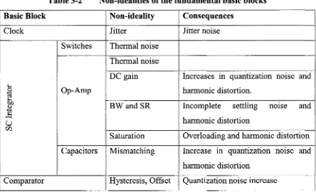
Table 3-2 Non-idealities of the fundamental basic blocks
Basic Block Non-ideality Consequences
Clock Jitter Jitter noise
Switches Thermal noise
Thermal noise SC In te g ra to r Op-Amp
DC gain Increases in quantization noise harmonic distortion.
and
BW and SR Incomplete settling noise harmonic distortion
and
Saturation Overloading and harmonic distortion Capacitors Mismatching Increase in quantization noise
harmonic distortion
and
Comparator Hysteresis, Offset Quantization noise increase
3.6
ZA Modulators Non-Idealities
Table 3-2 compiles the fundamental basic blocks and the non-idealities
considered.
3.7
Clock Jitter Model
The effect of clock jitter, on a SC ZA modulator can be calculated based on the
l — ^ dui'dt
o
R a n d o m Z e ro -Q « ter J H erS M L D ev .
Wumiwr Hold
n n i ^
JM-*0
.Zaro*Of®r
H o ld I
Figure 3-6. Modeling a random sampling jitter
Clock jitter results in a non-uniform sampling and increases the total error power
in the quantizer output. The magnitude of this error is a function o f both the statistical properties of the jitter and the input signal to the converter. The error introduced when a sinusoidal signal with amplitude A and frequency f n is sampled at an instant, which is in error, by an amount 8 is given by:
x(t + S ) - x (f)« 27finSAcos{27fint) = S — x{t) (3-13)
dt
This effect can be simulated with SIMULINK by using the model shown in Figure 3-6,
which implements equation 3-13. Here, it is assumed that the sampling uncertainty 8 is gaussian random process with “delta” standard deviation. Whether oversampling is
helpful in reducing the error introduced by the jitter depends on the nature of the jitter. The jitter is assumed to be white, so the resultant error has uniform power spectral from 0
to f s/2, with a total power of (27rfindeltaA)212. In this case, the total error power will be
reduced by the oversampling ratio [54].
3.8
Integrator Noise Model
While the performance o f the theoretical XA modulator is on ly determ ined by the
The circuit noise to be dealt with in a ZA modulator is the noise injected into the
input summing node of the first integrator, since it is added directly to the input signal and appears in the output spectrum without any filtering. White noises from the rest of the integrators are attenuated by different powers of the oversampling ratio, depending on the position of the integrator, and can be neglected.
The circuit thermal noise generated in an integrator has two main origins, the white noise due to the resistance of the MOS switches and the op-amp noise of the input stage. These noise sources originate a broadband and sampled noise component at the
output of the integrator. These effects can be successfully simulated with SIMULINK using the model of a “noisy” integrator shown in Figure 3-7, where the coefficient b
represents the integrator gain, which, referring to the schematic of a single-ended SC integrator shown in Figure 3-8, is equal to Cs/Cf.. Each noise source and its relevant model will be described in the following sub-sections.
o — ► Jfjt)
IN
i - t
e r A E i *
k T f f i M s a e Mediator VC*J
E H - * OpN'-'iStr I— * — ■ n — I
Callift OfrAimp Noted C p A n ip N o te d I *5)^ ^ ' ,,Lirat Desssy ■+d!
i
Figure 3-7. Noisy integrator model
© -H
Gain fc
M )
kT/C noiM
►J1-R sn flo m z a r e - o p a e f N u m ber H o n
c T
- * o yffl
Figure 3-9. Modeling thermal noise (KT/C block)
3.8.1 Switch Thermal N oise (KT/C) M odel
A critical source of noise in the system is the KT/C noise injected into the first stage integrator of the modulator. As a result, the input capacitor must be large enough to counter the additive noise effect that results. Therefore the first key parameter is the
input sampling capacitor of the first integrator (Cs).
Thermal noise is caused by the random fluctuations of carriers due to thermal energy and presents even at equilibrium. Thermal noise has a white spectrum and wide band limited only by the time constant of the SCs or the bandwidths of the op-amps. Therefore, it must be taken into account for both the switches and the op-amps in the SC circuits. For instant, the sampling capacitor Cs in the single-ended SC integrator shown in Figure 3-8, is in series with a switch, with finite resistance Ron that periodically opens, sampling a noisy voltage onto the capacitor. The switch thermal noise voltage eT (usually
called KT/C noise) can be found by evaluating the integral [27]:
4KTRon _ kT
+ ( 2 ^ 0„ C j 2 Cs
(3-14)
Where K is the Boltzman constant and T is the absolute temperature
The switch thermal noise voltage ex is superimposed to the input voltage x(t) leading to:
x(t)- kT
Where n(t) denotes a gaussian random process with unity standard deviation and b is the integrator gain expressed as:
Equation (3-15) is implemented by the model shown Figure 3-9
Since the noise is aliased in the band from 0 to f s/2, its final spectrum is white with a
spectral density:
The first integrator will have two switched input capacitor, one carrying the signal and the other providing the feedback from the modulator output, each of them contributing to
the total noise power.
3.8.2 Op-Amp Noise M odel
Figure 3-10 shows the model used to simulate the effect o f the op-amp noise.
Here Vn represents the total RMS noise voltage referred to the op-amp input. Flicker (1/f) noise, wide-band thermal noise and dc offset, contribute to this value. The total op- amp noise power V2n can be evaluated, through circuit simulation, on the circuit of Figure 3-8 during d>2, by adding the noise contribution of all the devices referred to the op-amp
input and integrating the resulting value over the whole frequency spectrum. b = Cs/Cf
(3-16)
Random Zero-Order Noise
Number Hold std. Dev.
MATLAB
Function
^ Stew-Raie
!=ttf
Leakage
Unit Delay S aturation
O
y(t)
Figure 3-11. Real integrator model
3.9
Integrator Non-Idealities Model
The op-amp is the most critical component of the modulator, as its non-idealities causes an incomplete transfer of charge, leading to non-linearities. Key parameters that govern its behaviour are the noise, finite gain, finite bandwidth, SR, and saturation voltages. The SIMULINK model of an ideal integrator with unity gain is shown in the
inset of Figure 3-2. Its transfer function is expressed as:
H(z) = ~—~ r (3-17)
1 — z
Analog circuit implementation of the integrator deviate from this ideal behaviour due to several non-ideal effects. One o f the major causes of performance degradation in
SC ZA modulators, indeed, is due to incomplete transfer of charge in the SC integrators. This non-ideal effect is a consequence of the op-amp non-idealities, namely finite gain and bandwidth, SR and saturation voltages. These will be considered separately in the following subsections. Figure 3-11 shows the model of the real integrator including all the non-idealities.
3.9.1 D C Gain
leakage is that only a fraction of the previous output of the integrator (a) is added to each
new input sample. The transfer function of the integrator with leakage becomes:
1 - a z (3-18)
Therefore the dc gain HO becomes:
H„=H(
0) =
-i-1 - a (3-19)
The limited gain at low frequencies increases the in-band noise.
3.9,2 Bandwidth and Slew Rate
The finite bandwidth and the SR of the op-amp are modeled in Figure 3.11 with a building block placed in front of the integrator, which implements a MATLAB function.
The effect of the finite bandwidth and SR are related to each other and may be interpreted as a non-linear gain [55]. With reference to the SC integrator shown in Fig (3.8), the
evolution of the output node during the nth integration period (when 0 2 is on) is:
Where a is the integrator leakage, t is the time constant of the integrator expressed as:
x = 1/ (27t GBW)
Vs is defined as:
v /
(3-20)
V , = V „ ( n T - T / 2 )
The slope of this curve reaches its maximum value when t = 0, resulting in:
Two separate cases will be considered:
1. The value specified by equation 3-21 is lower than the op-amp SR. In this
case there is no SR limitation and the evolution of v0 fits equation 3-20.
2. The value specified by equation 3-21 is larger than SR. In this case, the op- amp is in slewing and, therefore, the first part of the temporal evolution o f v0 (for t<to) is linear with the slope SR. The following equations hold (assuming
to<T):
vo(0 = v0( n T - T ) + SRt\ t < t 0 (3-22)
vo(t) = vo(to) + {a V s ~ S R t 0;\1 - e T 1 t > t0 (3-23)
V
Imposing the condition for the continuity of the derivatives of equation 3-22 and 3-23 in to, we get:
a V
t0 = - ^ - r (3-24)
0 SR
If t0 > T only Equation.3-22 holds.
The MATLAB function in Figure 3-11 implements the above equations to calculate the value reached by v0(t) at time T, which will be different from Vs due to the gain, bandwidth and SR limitations of the op-amp. The SR and bandwidth limitations produce
harmonic distortion reducing the total SNDR of the XA modulator. Appendix A. 1 shows
3.9.3 Saturation
The dynamic of signals in a ZA modulator is a major concern. It is therefore
important to take into account the saturation levels of the op-amp used. It can simply be
done in SIMULINK using the saturation block inside the feedback loop o f the integrator, as shown in Figure 3-11
3.10 Capacitor Mismatching
One of the main advantages of SC circuits is that high precision can be obtained as the integrator coefficients are realized with capacitor ratios. However, fabrication
process still results in capacitor mismatching and causes error to the values of these coefficients [56]. Consequently the quantization noise increases. In [53], it is shown that
single-loop ZA modulator can tolerate this type of error to as large as 5%. This is one of
the advantages for selecting single-loop, second-order topology, rather than the cascaded
topology.
3.11 Comparator
The principle design parameter of a comparator include speed, input offset, input-
referred noise, and hysteresis. Owing to its position in a Z A modulator, the offset and
input-referred noise are subjected to noise shaping by feedback loop so can be neglected. For digital-audio design, speed is also not a problem. The sensitivity of an A/D converter performance to comparator hysteresis can be modeled quite well by an additively white noise. This noise also undergoes the same spectral noise shaping as the quantization
noise. Thus the design requirement for the comparator is usually quite relaxed.
3.12 Behavioral Simulation for the Ideal ZA modulator
Behavioral simulation can be accomplished using SIMULINK tool, as it provides a GUI tool so the designer can easily build block diagram, perform simulation, and view the simulation results at each point. The necessary functions and programs can be written in MATLAB to measure the performance of the modulator. Figure 3-12 shows the block
fundamental blocks are the ideal integrator, single-bit quantizer, adders and multipliers.
Through adequate connections of these few blocks, a full £A modulator can be obtained.
Scopes are used to monitor all of the critical points. Figure 3-13 shows the input
sinusoidal, the outputs of the integrators and the modulator output superimposed on the input and the second integrator output. Figure 3-14 shows the normalized power spectral density at the output with 0.23 V input sinusoidal signal. By setting the different integrator coefficients and performing simulation, it is possible for the designer to choose the integrator coefficients that maximize the integrator output swing. However, owing to the use of ideal building blocks for the modulator, the simulation results cannot be very accurate and need to be fine-tuned by further behavioral simulation by using the blocks
that model non-idealities in Chapter 5.
n V in
S c o p e 2
□
□
S c o p e l
0 .5
y o u t
1 -z ' 1 - z ’
IDEAL I n te g r a to r !
y o u t IDEAL
In te g r a to r
j p ^LPl ft 1 ESI £ j
ta Modulat I TTTTTI
:i
SNR"nvf 100.1tiB@OSKf2i T--rNrTi-rrriT‘S a m p l i n g J i t t e r V i n
J it te r
y o u t 1-z"
R E A L In te g r a to r
y o u t R e la y
ID EA L In te g r a to r O p N o is e
kT/C
Figure 3-15. SIMULINK model for the non-ideal second-order EA modulator
3.13
Behavioural Simulation for the Non-Ideal EA modulator
The behavior of XA modulator can be affected by errors. The integrator is a
fundamental block within a XA modulator. Its non-idealities, however, largely affects the
operation of the modulator. The non-ideality for the first integrator only is considered, since their effects are not attenuated by the noise shaping. A single-bit quantizer is implemented with a comparator, which is a perfectly linear block and does not introduce any non-linearity error. Though linear block, comparators are subject to non-idealities
such as input offset, comparator hysteresis, etc. However, due to its position in the XA
modulators, the impact of the comparator non-idealities in the operation of XA
modulators is much smaller than of integrators as these errors are subject to the same treatment as quantization noise.
Figure 3-15 shows the blocks used to simulate the behavior of the second-order
SC XA modulator with a non-ideal first integrator [57]. To validate the models of the
various non-idealities affecting the operation of the SC XA modulator, several simulations are performed with SIMULINK on the second-order modulator of Figure 3- 15
integrator coefficients and building block parameters so as to design a XA modulator with the best possible performance.
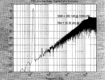
For this design, after intensive simulation with SIMULINK and running the necessary programs, the SNDR curve that is believed to be the best outcome is shown in Figure 3-15. Within which, a 96 dB peak SNDR and 98 dB DR are achieved. The
simulated PSD is shown in Figure 3-17 with -2 dB input sin signal. Fig 3.17 shows that the noise floor is well under -100 dB for an input signal as big as -2 dB and the modulator is thermal noise dominated. The corresponding modulator coefficients and building blocks parameters that result in the above performance are listed in Table 3-3 and 3-4.
S N D R fat ’ lie Behavioural Simulation
100
DFj = 98; Resolution = 16 bjts
OvStaad Level=G.26V
■20
-BD ■GO ■A'i
Inpul Signal Amplilude [dB]
-100
PSD of a 2nd-Order Sigma-Delta Modulator
-20
S N R H 9 6 .3 d B @ iQ S R fl: -40
-60
-80
' -100
-140
-160
-180
-200
Frequency [Hz]
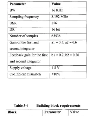
Table 3-3 Second-order modulator coefficients and parameters
Parameter Value
BW 16 KHz
Sampling frequency 8.192 MHz
OSR 256
DR 16 bit
Number of samples 65536
Gain o f the first and second integrator
al = 0.5; a2 = 0.6
Feedback gain for the first and second integrator
b l = 0.2; b2 = 0.26
Supply voltage 1.8 V
Coefficient mismatch <10%
Table 3-4 Building block requirements
Block Parameter Value
Op-Amp Gain >55 dB
GBW >40 MHz
SR >16V/us
Output swing 0.1-1.7V
Chapter 4
Low- Voltage Low-Power Design Considerations
When an analog integrated circuit is needed at low supply voltage levels, the SC
technique is the only technique in CMOS that can be used in practice to achieve good
quality circuit. Probably the most robust way to implement a £A modulator is with SC
technique. Their robustness and inherent linearity are the reasons why SC techniques have become as widespread as they are nowadays. It would be a great advantage if the high-quality SC properties could be kept for low voltage operation. However, when
designing SC circuits for lower voltages, quite quickly a sever difficulty is encountered due to the switch-driving problem. The low supply voltage does not allow enough overdrive to turn on the transistors used as switches anymore, and SC circuits at low voltages could only be realized either in a special process with extra low threshold voltage transistors or by using an on-chip voltage multiplier. The SO technique, derived from the standard SC technique, is based on the replacement of critical switches with op- amps, which are turned on and off. This technique results in a true very low-voltage operation and can be used in a standard CMOS process.
It is plausible that a circuit with a higher frequency of operation requires a higher power. It is also plausible that performing analog signal processing with increased
accuracy requires increased power consumption. So if a certain performance requires certain power consumption, altering the performance through a redesign should change the necessary power consumption. The proper way to think about low power consumption is to define it as a trade off between contradictory specifications, such as accuracy, frequency of operation or signal bandwidth and power consumption. Lowering the power supply at first looks like it lowers the power consumption because the product of voltage and current is smaller. However, lowering the power supply voltage has a number of consequences that on the contrary cause the power consumption to increase, as will be shown and illustrated further on.
the switches. The existing solutions for it are briefly covered. Then the original SO principle is introduced. Next the evolution in this field is described. The endpoint is the differential modified SO integrator cell. Low-voltage, low-power considerations are then
discussed in the context of the single loop XA modulator.
4.1
Switch Behavior
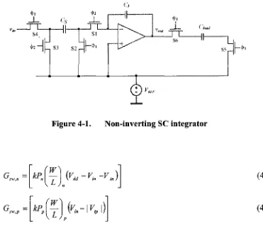
SC circuits are built up of three basic building blocks. An op-amp or an operational transconductance, a switch and a capacitor. Figure (4-1) shows a non inverting integrator cell. The switches SI through S6 are clocked with two non
overlapping phases <|)1 and <|>2. Cs is the input sampling capacitor, Q is the integrating
capacitor and Cmad is the load capacitor. Lowering the supply voltage of such a circuit has implications on the operation of some of the building elements. The functional
property o f a capacitor, namely its capacitance is independent of the supply voltage. Op- amps and switches, however, are strongly affected. The former need to cope with much less available voltage drop over each transistor. The later always need a minimal
overdrive voltage in order to assure a certain on-resistance. It is possible to design op- amp with quite low supply voltage [58]. The most problematic issue, however, in low voltage SC circuits deign is the switching driving problem. About (Vm +Vtp + 0.5 V) is the practical minimal power supply voltage for the switch still has rail-to-rail switch input
range [59] [60].