Design of 900 Mhz AC to DC Converter Using Native
Cmos Device of TSMC 0.18 Micron Technology for RF
Energy Harvest Application
Angelo N. Rodriguez
1,*, Febus Reidj G. Cruz
2, Ronnie Z. Ramos
31School of Graduate Studies, Mapua Institute of technology, Manila, Philippines
2School of Electrical Electronics and Computer Engineering, Mapua Institue of Technology, Manila, Philippines 3Maritime Academy of Asia and the Pacific, Mariveles, Bataan, Philippines
Copyright © 2015 by authors, all rights reserved. Authors agree that this article remains permanently open access under the terms of the Creative Commons Attribution License 4.0 International License.
Abstract
RF signal carries very low amount of energy and can be easily dissipated as heat loss. Threshold voltage and leakage current that are inherent in MOS transistors significantly affect the performance of an RF AC to DC converter. A device with bulk connected to its drain improves the threshold voltage and leakage current. This work designs the half-wave and full-wave AC to DC converters with devices’ bulk connected to source and devices’ bulk connected to drain. The designs used the native devices in TSMC 0.18 micron CMOS technology, and were simulated using transient analysis in different process corners and operating temperatures. In simulations, the RF signal was represented by a sinusoidal input of 900 MHz frequency and of 390 mV amplitude. The sizes of transistors and the number of stages, of each converter, that resulted to highest power efficiency were determined via circuit simulations. The optimal design was a four-stage half-wave AC to DC converter with devices’ bulk connected to drain, which produced a DC output of 2.7 V with 37.42 % efficiency at 100 kilo ohm load.Keywords
RF Energy Harvest, AC to DC Converter, Native MOSFET, Bulk-drain Connection1. Introduction
Today’s technology allows electronic devices to be operated at low input voltages. These low power devices can be used in many applications such as temperature sensors, pressure sensors, biomedical sensors and RFID systems. The battery can be used as a source for these low power devices; however, battery has finite life and need to be changed periodically. Harvesting environmental energy can extend the battery life and minimize cycle of disposing and replacing of battery. The RF signals carry a small amount of energy which can be stored in a battery to operate low power devices by means of RF energy harvesting device.
The input RF signal that will undergo RF to DC
conversion must have minimal loss and must be greater than the magnitude of the input signal. Schottky diodes are commonly exploited component in a RF to DC converter circuit [1]; however, production cost may increase because of the non-standard CMOS process [2].An alternative solution for this problem is to use diode connected CMOS. The problem arises in using diode connected CMOS transistor is the threshold voltage of the transistor itself. The works of Mandal et al. [3] to Shokrani et al. [8] proposes several threshold cancellation techniques to minimize the effect of the turn on voltage of the CMOS device. In 2012, works of Lin et al. [7] exploited the use of native CMOS device in lowering the threshold voltage of the transistor. However, the drawback of using a low threshold voltage device is the increase in leakage current. This current should be minimized because it decreases the overall output voltage and efficiency of the circuit. A simpler leakage current prevention technique is used by Shokrani et al. [8] in which was done by connecting the bulk to the drain of MOS transistor.
This study aims to design an AC to DC converter for 900 MHz RF energy harvester circuit using Native CMOS device with proper connection of bulk. The second section presents a characterization of the threshold voltage and leakage current of native MOSFET devices in TSMC 0.18 um CMOS process. The third section is the design of an AC to DC converter base on multi stage half-wave rectifier using native CMOS device with bulk connected to source and bulk connected to drain. The fourth section of this paper is the design of AC to DC converter base on multistage full-wave rectifier with bulk connected to source and bulk connected to drain. It also includes the summary and the final design base on the gathered data.
2. Characterization of Threshold
The transistors that were utilized in this work were characterized to determine the actual threshold voltage and the leakage current. The threshold voltage was determined through linear extrapolation technique [9]. The linear extrapolation method was done by measuring the drain current as a function of gate voltage.
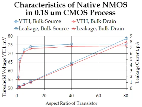
The characterization procedure done in this work included the comparison of the threshold voltage and leakage current for the bulk connected to drain and bulk connected to source. According to Shokrani & et al. [8], the threshold voltage is minimized by connecting the bulk to the drain. The threshold voltage when the bulk of a MOS transistor was connected to drain at TT process corner and 25 oC varies from 54 mV to
[image:2.595.314.551.238.337.2]74 mV while for bulk connected to source it varies from 56 mV to 76 mV as shown in Fig. 1.
Figure 1. Threshold voltage and leakage comparison of native NMOS with bulk connected to source and bulk connected to drain at 20oC across TT process corner.
The lowering of threshold voltage was due to the reason that when a positive voltage is applied to the MOS transistor, the source to bulk voltage becomes negative as described in Equation 3 [8]. The works of Shokrani et al. [8] in 2012 also stated that the leakage current will be decreased when the bulk of the transistor is connected to the drain. This effect was graphically shown in Fig. 1 and can be described by Equation 2. During reverse bias region, the source to bulk voltage became positive resulting to an increase in threshold voltage VTH.
(1)
(2)
3. Design of Ac-Dc Converter Using
Multi-Stage Half-Wave Rectifier
The design of AC to DC converter based on multi-stage half-wave rectifier implemented the principle of voltage doubler. Moreover the design utilized the native CMOS device which is available in TSMC 0.18 um CMOS process and two bulk connections; bulk connected to source and bulk connected to drain. The source voltage for a 900 MHz frequency is set to 390 mV [10]. The design procedure is shown in Fig. 2 and the efficiency is computed by dividing the dc output power (PDC) to the ac input power (Pac) as
[image:2.595.58.298.263.444.2]shown in Equation 3.
Figure 2. Design procedure for half-wave and full-wave AC-DC converter.
(3)
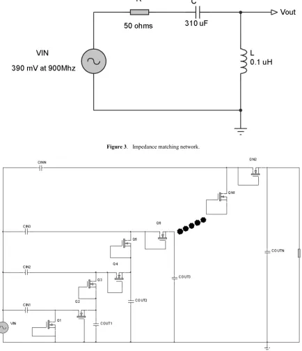
A simple RLC resonant circuit shown in Fig. 3 is connected at the input of the multi stage half wave rectifier design to improve the available voltage at the input of the rectifier and provide higher power transfer. This resonant circuit is tuned using Equation 4 and 5.
(4)
(5)
Figure 3. Impedance matching network.
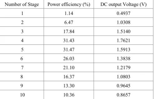
Figure 4. N-stage AC to DC converter based on multi-stage half-wave rectifier with bulk connected to source
As the stages were added to the design, the efficiency improves due to an increase in the DC output voltage but it reaches a maximum point and begun to decrease as shown in Table I. The transistors’ efficiency peaks at 4 to 5 stages. Increasing the number of stages would result to an increase in the number of components, hence the power loss due to leakage current and super threshold region would also increase in proportion to the number of stages as describe in Equations 8, 9, and 10 [12]. Psub1 and Psub2 are the power due
to subthreshold region, Psup is the power due to
superthreshold region and Pleak is the power loss due to
leakage current. In this case, a five stage with W/L = 40 was chosen in the design of half-wave multi-stage multiplier with bulk connected to source because it gives the maximum overall efficiency of 31.47 %, output voltage of 1.59 V, and output current of 0.57 uA at load of 100 kΩ.
(6)
(8)
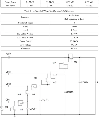
Table 1. Power efficiency and DC output voltage with varying stages, W/L = 40 , Half –wave, bulk connected to source
Number of Stage Power efficiency (%) DC output Voltage (V)
1 1.14 0.4937
2 6.47 1.0308
3 17.84 1.5140
4 31.43 1.7621
5 31.47 1.5913
6 26.03 1.3838
7 21.10 1.2179
8 16.37 1.0803
9 13.30 0.9645
10 10.36 0.8657
Table 2 shows the result for the n-stage half-wave rectifier with bulk connected to drain. The optimum size in this case was a four stage circuit with W/L=20. It gives a maximum overall efficiency of 37.42% with output voltage of 2.7V and output current of 27.01 uA at load R1 = 100 kΩ.
Table 2. Power efficiency and DC output voltage with varying Stages, W/L=20, Half-Wave, Bulk connected to Drain
Number of Stage Power efficiency (%) DC output Voltage(V)
1 13.35 3.3312
2 28.88 3.6289
3 35.27 3.1282
4 37.42 2.10013
5 34.32 2.2678
6 30.78 1.9574
7 27.50 1.7258
8 23.88 1.5323
9 19.82 1.3604
10 17.44 1.2430
4. Design of Ac-Dc Converter Using
Multi-Stage Full-Wave Rectifier
The design of the AC to DC converter based on multi-stage full-wave rectifier was based on the design of the half-wave AC to DC converter. An additional NMOS diode
connected MOS transistor circuit was used to allow conduction on the other half cycle.
Referring to Table 3, the efficiency increases as the second and third stage were added but started to drop when fourth and fifth stages were also added. The drop in efficiency was expected because of the power loss exhibited by the added transistors. The W/L ratio that gives the maximum efficiency is W/L=30 at 22.89 % efficient. It also gives an output voltage of 1.98 V and output current of 19.81 uA for load of 100 kΩ.
Table 4 shows the result for full-wave design with bulk connected to drain. The schematic is similar with Fig. 5 but the bulk connection was transferred to the drain. The W/L ratio that gave the highest efficiency and good amount of voltage was a three stage circuit with W/L=30 at 24.29 % efficient. It has an output voltage of 2.03 V and output current of 20.31 uA for load 100 kΩ.
Table 3. Power efficiency and DC output voltage with varying the number of stages, W/L = 30, Full – wave, bulk connected to source
Number of Stage Power efficiency (%) DC output Voltage (V)
1 19.47 0.8543
2 22.14 1.4645
3 22.89 1.9813
4 22.27 2.4157
5 21.42 2.7942
Table 4. Power efficiency and DC output voltage with varying the number of stages, W/L = 30, full – wave, bulk connected to drain
Number of Stage Power efficiency (%) DC output Voltage (V)
1 21.46 0.8716
2 23.74 1.4986
3 24.29 2.0307
4 23.48 2.4782
5 22.50 2.8684
5. Summary of Results
Table 5. Summary of the results for both half – wave and full – wave AC to DC converter
Parameter Bulk connected to Half –Wave Full –Wave
source Bulk connected to drain Bulk connected to source Bulk connected to drain
Number of Stages 4 4 2 2
DC Output Voltage 1.59 V 2.70 V 1.98 V 2.03 V
DC Output Current 0.57 uA 27.01 uA 1981 uA 20.31 uA
Output Power 25.57 uW 73.74 uW 39.35 uW 41.33 uW
[image:5.595.112.502.167.632.2]Efficiency 31.47% 37.42% 22.89% 24.29%
Table 6. 4-Stage Half-Wave Rectifier as AC-DC Converter
Parameter Half –Wave
Bulk connected to drain
Number of Stages 4
Width 10 um
Length 0.5 um
DC Output Voltage 2.100 V
DC Output Current 27.01 uA
Output Power 73.74 uW
Input Voltage 390 mV
Efficiency 37.42%
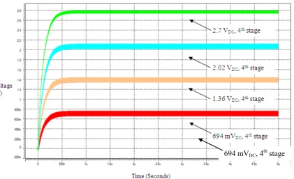
Figure 5. 4-stage half-wave AC-DC converter with bulk connected to drain
Figure 6. Output voltage across each stage of 4-stage half-wave AC-DC converter with bulk connected to drain
6. Conclusions
This work designed 900 MHz AC to DC converters using native devices in TSMC 0.18 micron CMOS technology. Native NMOS with bulk connected to drain yielded lower threshold voltages and lower leakage currents, as compared to native NMOS with bulk connected to source. At room temperature, typical process, and device size of 10, native NMOS with bulk-drain connection had 72.9 mV threshold and 1.08 pA leakage, while native NMOS with bulk-source connection had 74 mV threshold and 1.18 pA leakage. Four designs were implemented in this study, namely: (Design 1) multi-stage half-wave rectifier with bulk-source connected native devices, (Design 2) multi-stage half-wave rectifier with bulk-drain connected native devices, (Design 3) multi-stage full-wave rectifier with bulk-source connected native devices, and (Design 4) multi-stage full-wave rectifier with bulk-drain connected native devices. Input RF signal was simulated using 900 MHz and 390 mV sinusoidal voltages. Optimum number of stages in each design was determined, and simulations showed that highest efficiency was achieved in 4 stages for half-wave rectifiers and 2 stages for full-wave rectifiers. Among the four designs, the 4-stage half-wave rectifier with bulk-drain connection yielded the highest output of 2.7 V with highest efficiency of 37.42% at 100 kΩ.
REFERENCES
[1] Nintanavongsa P., Muncuk, U., Richard, D., Kaushik, L., & Chowdhury, R., Design Optimization and Implementation for
RF Energy Harvesting, IEEE Journal on Emerging and Selected Topics in Circuits and Systems ,Vol. 2,No. 1, pp24-33, 2012.
[2] Yuan, F., CMOS Circuits for Passive Wireless Microsystems, Springer, pp 7-47, 2011.
[3] Mandal, S., & Sarpeshkar, R., Low-Power CMOS Rectifier Design for RFID Applications, IEEE Transactions on Circuits and Systems, Vol. 54, No. 6, pp 1177-1187, 2007.
[4] Feldengut T., R. Kokozinski,& S. Kolnsberg, A UHF Voltage Multiplier Circuit Using a Threshold-Voltage Cancellation Technique, IEEE Journal, Vol. 9, pp 288-291, 2009.
[5] Ebrahimian, M., El-Sankary K., & El-Masry, E., Enhanced RF to DC CMOS Rectifier with Capacitor-Bootstrapped Transistor, IEEE Journal, Vol. 10, pp 1655-1658, 2010. [6] Raben, H., Borg, J., &Johansson, J., Improved Efficiency in
the CMOS Cross – Connected Bridge Rectifier for RFID Application., 18th International Conference “Mixed Design of Integrated Circuits and Systems”, pp 334-339, 2011. [7] Lin, G., Lee,M., & Hsu. Y., An AC – DC Rectifier for RF
Energy Harvesting System, Proceedings of APMC, pp 1052 – 1054, 2012.
[8] Shokrani, M. R., Hamidon, M. N., Khoddam, M., &Najafi, V., A UHF Micro-Power CMOS Rectifier Using a Novel Diode Connected CMOS Transistor for Micro-Sensor and RFID Applications, IEEE International Conference on Electronic Design, System and Applications (ICEDSA), pp 235-238, 2012.
[9] D. Schroder. Semiconductor Material and Device Characterization, Prentice Hall, Lake Street, Upper Saddle River, New Jersey, 07458, 2006.
[10] Karolak, D.,Taris, T., Begueret, J., & Mariano, A., Design Comparison of Low-Power Rectifiers Dedicated to RF
Energy Harvesting. IEEE Journal, Vol. 12, 524-527, 2012. [11] Yan, H.,Montero, J.,&Akhnoukh, A. (2005).An Integration
Scheme for RF Power Harvesting. IEEE.