Department of Electrical & Electronics Engineering, College of Engineering Perumon, Kollam, Kerala – 691601, India
Interleaved Boost Converter with a Voltage
Multiplier for PV Module Using Grid
Connected Load in Rural Areas
K A Yamuna
Dept. of Electrical and Electronics, Rajiv Gandhi Institute of Technology, Pampady, Kottayam, Kerala, India
ABSTRACT: In the existing system having step-up converters, such as the boost converter and fly back converter, it is
not possible to achieve a high step-up conversion with high efficiency because of the resistances of elements or leakage inductance. Conventional step-up converters with a single switch are un-suitable for high-power applications which gives an input large current ripple, which increases conduction losses. Thus numerous interleaved structures and some asymmetrical interleaved struc-tures are extensively used. The step up converter with voltage multiplier is an asymmetrical interleaved converter for a high step-up gain , which is suitable for high-power application. The voltage multiplier module is composed of a conventional boost converter and coupled inductors. Through this voltage multiplier module, a high step-up gain is obtained without operating at an extreme duty ratio. For achieving a high voltage conversion ratio, an extra conventional boost converter is introduced. The two-phase configuration reduces the current stress through each power switch and input current ripple, which decreases the conduction losses of MOSFETs. Since the energy stored in leakage inductances is recycled to the output terminal, efficiency can be improved.
KEYWORD: Photo voltaic system ,boost converter,voltage mul-tiplier.
I. INTRODUCTION
Regardless of the intermittency of sunlight, solar energy is widely available and is free. Recently, photovoltaic system is recognized to be in the forefront in renewable electric power generation [1]. It can generate direct current electricity without an environmental impact and contamination when exposed to solar radiation. Being a semiconductor device, the PV system is static, quiet, free of moving parts, and has little operation and maintenance costs. PV module represents the fundamental power conversion unit of a PV generator system. The output characteristics of a PV module depend on the solar insolation, the cell temperature and the output voltage of the PV module. Since PV module has non linear characteristics, it is necessary to model it for the design and simulation of maximum power point tracking (MPPT) for PV system applications.
Department of Electrical & Electronics Engineering, College of Engineering Perumon, Kollam, Kerala – 691601, India
Fig. 1. Typical pv system with grid connected load
Conventional step-up converters with a single switch are unsuitable for high power applications given an input large current ripple, which increases conduction losses. Thus, nu-merous interleaved structures and some asymmetrical inter-leaved structures are extensively used Due to several reasons such as parasitic components, the requirement of a high duty cycles,conventional DC-DC converters can not achieve a high voltage gain. Many topologies have been proposed to overcome these disadvantages with high voltage gain without the use of high duty cycles. Converters with transformers provide high voltage gain a low voltage stress on the active switch, and a high efficiency without the increase of high duty ratio. The transformer can be replaced with coupled inductors to reduce the conduction or core losses in the system.
A voltage multiplier is an electrical circuit that converts power from lowervoltage to a higher DC voltage. Interleaved structure is employed in the input side to reduce the input cur-rent ripple and improve the power level. The voltage multiplier circuit is adopted in the output side to achieve a high step-up voltage gain and simplify the circuit structure. The voltage multiplier circuit is composed of capacitors, diodes, and two coupled inductors, which can extend the voltage gain and minimize the current ripple without extreme duty cycle. Switch voltage stress is reduced as the turns ratio of the coupled inductors increases, which makes low-voltage rated MOSFETs available to improve the circuit performance. The diode reverse recovery problem can be alleviated by the leakage inductance of the coupled inductors, which reduces the reverse recovery losses. The use of power Metal Oxide Semiconductor Field Effective Transistor( MOSFETs) and diodes makes the circuit working at higher frequencies of range 40 kHz, resulting in a reduced value of the capacitance required in the capacitor diode voltage multiplier connecting boost converter. The high step up DC-DC converter with coupled inductor and voltage multiplier is discussed in this report. The fig 1.1 shows a typical photovoltaic system connecting to dc-dc converter, inverter and load [1] .
II. OPERATING PRINCIPLE DESCRIPTION
The step up converter is a non-isolated topology for boosting low voltage input to high voltage output. The input current are usually continuous in nature and is supplied to the load by either the conduction of diodes or capacitors. The boost converter with voltage multiplier by means of coupled inductor insertion increases the output voltage, hence the voltage gain and efficiency, with low value of duty cycle. The output voltage across the load is the sum of the voltage from boost converter and the voltage across the voltage multiplier capac-itors. The required duty cycle can be obtained by adjusting the voltage multiplier, which increases the output voltage. An asymmetrical interleaved high step-up converter that combines the advantages of both conventional boost converters and voltage multiplier is discussed is shown in fig 1.(a). The voltage gain can be extended by voltage lift capacitor and voltage multiplier connected in the circuit. The voltage lift capacitor connected to the boost converter increases the output voltage. The converter works in continuous conduction mode of operation. The power is delivered to the load during both ON and OFF states. The active clamp circuits are in builds on the converter for high voltage conversion.
Department of Electrical & Electronics Engineering, College of Engineering Perumon, Kollam, Kerala – 691601, India
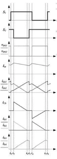
Mode 1: Initially t=t0 , the switches S1 and S2 are both turned ON and all diodes are reversed-biased. The input voltage Vin charges the magnetizing inductors Lm1 and Lm2 linearly. Also the charges leakage inductors Lk1 and Lk2.
Mode 2: At instant t=t1 , the switch S2 is switched OFF, diodes D2 and D4 become forward biased. The energy that magnetizing inductor Lm2 has stored is released to the secondary side of coupled inductor charging the output filter capacitor C3. The input voltage source, magnetizing inductor Lm2 , leakage inductor Lk2 , and voltagelift capacitor Cb transfer energy to the output filter capacitor C1 via diode D2 , increases the voltage on C1.
Fig. 2. (a)Proposed converter with voltage multiplier module and (b)Equivalent circuit of proposed converter
Fig. 3. (a)Triggering pulses of proposed converter
Mode 3: At instant t=t2, the diode D2 turn OFF because the total energy stored in the leakage inductor Lk2 is completely released to the output filter capacitor C1. Magnetizing inductor Lm2 release energy to the secondary side charging the output filter capacitor C3 through diode D4.
Mode 4: At instant t=t3, the switch S2 is switched ON and all the diodes get reverse biased.
Mode 5: At instant t=t4, the switch S1 is turned OFF, which turns ON diodes D1 and D3 . The energy stored in magnetizing inductor Lm1 is transferred to the secondary side charging the output filter capacitor C2 . The input voltage source and magnetizing inductor Lm1 transfer energy to voltage-lift capacitor Cb via diode D1 , which stores extra energy in Cb .
Department of Electrical & Electronics Engineering, College of Engineering Perumon, Kollam, Kerala – 691601, India
Some assumptions are made for the analysis of the con-verter: 1. All of the components are ideal 2. Leakage inductors Lk1 and Lk2 are neglected [4]. 3. Voltage Vcb, Vc1, Vc2 , and Vc3 are considered to be constant because of their large values.
Fig. 4. mode of operation of proposed converter.(a)Mode1(b)Mode2 (c)Mode3(d)Mode4 (e)Mode5 (f)Mode6
Figures 4. shows the various modes of operation of converter with voltage multiplier [5].The fig 3.(a) shows a triggering pulses of the converter.
A. SIMULATION OF HIGH BOOT CONVERTER WITH VOLTAGE MULTIPLIER
Department of Electrical & Electronics Engineering, College of Engineering Perumon, Kollam, Kerala – 691601, India
components selection and coupled inductor design [1]s. Due to the performance of high step up gain the turns ratio are set as 1:1. The boost converter with voltage multiplier can be efficiently implemented for step up conversion without extreme duty cycle [6].
Fig. 5. Waveform of proposed converter
TABLE I CONVERTER COMPONENTS AND PARAMETERS
Parameters Symbols Specification
Input voltage Vin 30v
Output voltage Vout 300v
Turns Ratio n(Ns/Np) 1
Switiching frequency fs 40khz
Load R 200W
Capacitor c1 470microF
Capacitor c2 220microF
Capacitor c3 220microF
Diode D1,D2,D3 IN4007
Department of Electrical & Electronics Engineering, College of Engineering Perumon, Kollam, Kerala – 691601, India
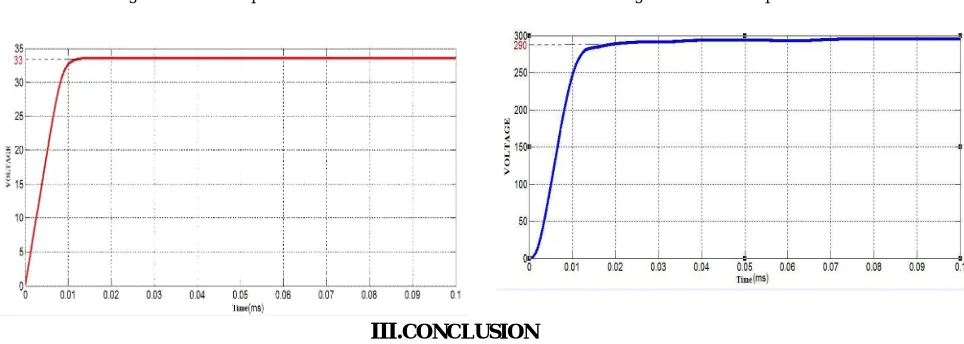
Fig. 6. Simulation input Result Fig. 7. Simulation output Result
III.CONCLUSION
REFERENCES
[1]K. C. Tseng, C. C. Huang, and W. Y. Shih, “A high step-up converter with a oltage multiplier module for a photovoltaic system,” IEEE Transactions on Power Electronics, vol. 28, no. 6, pp. 3047–3057, June 2013.
[2]K. C. Tseng and T. J. Liang, “Novel high-efficiency step-up converter,” IEE Proceedings - Electric Power Applications, vol. 151, no. 2, pp. 182– 190, Mar 2004.
[3]H. Ghoddami and A. Yazdani, “A single-stage three-phase photovoltaic system with enhanced maximum power point tracking capability and increased power rating,” IEEE Transactions on Power Delivery, vol. 26, no. 2, pp. 1017–1029, April 2011.
[4]W. Li, Y. Zhao, J. Wu, and X. He, “Interleaved high step-up converter with winding-cross-coupled inductors and voltage multiplier cells,” IEEE Transactions on Power Electronics, vol. 27, no. 1, pp. 133–143, Jan 2012.
[5]C. M. Lai, C. T. Pan, and M. C. Cheng, “High-efficiency modular high step-up interleaved boost converter for dc-microgrid applications,” IEEE Transactions on Industry Applications, vol. 48, no. 1, pp. 161–171, Jan 2012.
[6]J. M. Carrasco, L. G. Franquelo, J. T. Bialasiewicz, E. Galvan, R. C. PortilloGuisado, M. A. M. Prats, J. I. Leon, and N. Moreno-Alfonso, “Power-electronic systems for the grid integration of renewable energy sources: A survey,” IEEE Transactions on Industrial Electronics, vol. 53, no. 4, pp. 1002–1016, June 2006.