University of Windsor
University of Windsor
Scholarship at UWindsor
Scholarship at UWindsor
Electronic Theses and Dissertations
Theses, Dissertations, and Major Papers
1-1-2007
FPGA implementation of a wireless sensor node.
FPGA implementation of a wireless sensor node.
Junsong Liao
University of Windsor
Follow this and additional works at:
https://scholar.uwindsor.ca/etd
Recommended Citation
Recommended Citation
Liao, Junsong, "FPGA implementation of a wireless sensor node." (2007). Electronic Theses and
Dissertations. 7110.
https://scholar.uwindsor.ca/etd/7110
F P G A Im plem entation of A W ireless Sensor N ode
by
J u n s o n g L iao
A Thesis
Submitted to the Faculty of G raduate Studies
through Electrical and Computer Engineering
in P artial Fulfillment of the Requirements for the
Degree of M aster of Applied Science at the
University of Windsor
1*1
Library and
Archives Canada
Published Heritage
Branch
395 W ellington Street Ottawa ON K 1A 0N 4 Canada
Bibliotheque et
Archives Canada
Direction du
Patrimoine de I'edition
395, rue W ellington Ottawa ON K 1A 0N 4 Canada
Your file Votre reference ISBN: 978-0-494-42242-7 Our file Notre reference ISBN: 978-0-494-42242-7
NOTICE:
The author has granted a non
exclusive license allowing Library
and Archives Canada to reproduce,
publish, archive, preserve, conserve,
communicate to the public by
telecommunication or on the Internet,
loan, distribute and sell theses
worldwide, for commercial or non
commercial purposes, in microform,
paper, electronic and/or any other
formats.
AVIS:
L'auteur a accorde une licence non exclusive
permettant a la Bibliotheque et Archives
Canada de reproduire, publier, archiver,
sauvegarder, conserver, transmettre au public
par telecommunication ou par Nntemet, preter,
distribuer et vendre des theses partout dans
le monde, a des fins commerciales ou autres,
sur support microforme, papier, electronique
et/ou autres formats.
The author retains copyright
ownership and moral rights in
this thesis. Neither the thesis
nor substantial extracts from it
may be printed or otherwise
reproduced without the author's
permission.
L'auteur conserve la propriete du droit d'auteur
et des droits moraux qui protege cette these.
Ni la these ni des extraits substantiels de
celle-ci ne doivent etre imprimes ou autrement
reproduits sans son autorisation.
In compliance with the Canadian
Privacy Act some supporting
forms may have been removed
from this thesis.
While these forms may be included
in the document page count,
their removal does not represent
Conformement a la loi canadienne
sur la protection de la vie privee,
quelques formulaires secondaires
ont ete enleves de cette these.
© 2007 Junsong Liao
All Rights Reserved. No Part of this document may bo reproduced, stored or otherwise retained in
a retrcival system or transm itted in any form, on any medium by any means without prior written
A b stra ct
Real world wireless sensor network applications impose a wide range of constraints on the system
platforms, such as size, cost, power consumption, performance and flexibility. Therefore, sensor
network platforms tend to be application specific rather than general purpose. However, most aca
demic research today still uses general CPU-based embedded systems as sensor network platforms.
Although CPU-based sensor nodes are flexible and convenient for developing sensor network appli
cations, they are inefficient in handling event-driven tasks and consequently consume more energy.
Custom hardware, on the other hand, is more efficient in handling event-driven tasks, but less flex
ible th an CPU-based platforms. In this thesis, a hardware-based sensor network node is presented
as an alternative sensor network application platform capable of leveraging the event-driven nature
of sensor network applications. The implementation is based on Zigbee standard and is targeted for
the Xilinx Spartan3 FPGA. The FPG A implementation provides the flexibility of exploring design
space while keeping the performance of application specific hardware. Significant improvements arc
achieved by avoiding the overhead of operating system and interrupt handling. Compared to tradi
tional CPU-based sensor nodes, the hardware-based system has 3~11 times reduction in cycle count
A cknow ledgm ents
I would like to express my sincere gratitude for the invaluable guidance and constant support of
my supervisors, Dr. Mohammed A.S. Khalid and Dr. Kcmal E. Tepe. I would also like to express
my gratitude to other members of my committee Dr. Ziad Kobti and Dr. Jonathan Wu for their
kindness, flexibility and helpful comments.
I would like to thank my fellow graduate students of the ECE department for their support and
advice throughout the course of my study and research. Especially, I wish to thank Hongmei, Omar,
Marwan, Aws and Thuan for creating a friendly, encouraging research environment in the FPGA
C o n te n ts
A b s t r a c t iv
D e d ic a t io n v
A c k n o w le d g m e n ts v i
L ist o f F ig u r e s x
L ist o f T a b le s x ii
L ist o f A b b r e v ia tio n s x iii
1 I n tr o d u c t io n 1
1.1 Wireless Sensor N e tw o r k s ... 1
1.2 Thesis O b je c tiv e ... 5
1.3 Thesis Organization ... 6
2 B a c k g r o u n d a n d P r e v io u s W o rk 7 2.1 Dedicated Embedded Sensor S y s t e m ... 8
2.2 Dedicated Processor for Sensor Network A p p lic a tio n ... 11
2.3 Dedicated Architecture for Sensor Network Application ... 12
C O N T E N T S
3 S y s te m A r c h ite c tu r e 16
3.1 Event-Driven A rch itectu re ... 17
3.2 Hardware Acceleration ... 21
3.3 Parallel Distributed C o m p u ta tio n ... 21
3.4 System C o m p o n e n ts ... 22
3.4.1 Radio control u n i t ... 23
3.4.2 Parsing and classification u n i t ... 24
3.4.3 Network control u n i t ... 26
3.4.4 Application and management u n i t ... 28
3.4.5 Modification and framing u n i t e ... 29
3.4.6 CC2420 m o d u le... 29
4 Im p le m e n ta tio n an d R e s u lt s 30 4.1 Implementation Platform ... 30
4.1.1 RC10 development b o a r d ... 30
4.1.2 CC2400 evaluation board and CC2420 ... 33
4.2 Implementation Details ... 35
4.3 Test R e s u lts ... 35
4.3.1 Functional t e s t s ... 36
4.3.2 Packet error rate versus communication ra n g e ... 38
4.3.3 Crosstalk induced packet e r r o r ... 38
4.3.4 Performance analysis using execution cycle c o u n t ... 41
4.3.5 System th ro u g h p u t... 43
4.3.6 The trade-off of hardware-based s y s t e m ... 43
5 C o n c lu sio n a n d F u tu r e W o rk 45
R e fe r e n c e s 47
C O N T E N T S
A V H D L S o u r c e C o d e E x a m p le s 50
A .l Zigbee P a c k a g e ... 50
A.2 Zigbee Top M o d u le... 57
A.3 Radio Control U n i t ... 69
L ist o f F ig u res
1.1 Zigbee protocol a rc h ite c tu re ... 4
2.1 Dedicated embedded sensor node system arch itectu re... 9
2.2 Dedicated Embedded Sensor Node System A r c h ite c tu r e ... 10
2.3 SNAP a rc h ite c tu re ... 11
2.4 Evcnt-processor-based a rc h ite c tu re ... 13
2.5 Analysis of energy efficiency versus flexibility trade-off for a number of common ar chitectural styles (for a 0.25 micron CMOS process) [1]... 15
3.1 The Zigbee implementation system block diagram ... 17
3.2 Event driven a r c h ite c tu r e ... 18
3.3 Event handler state m achine... 19
3.4 Event handler state m achine... 20
3.5 Zigbee frame s tr u c tu r e ... 25
3.6 The input data and output frame format of parsing and classification u n i t ... 25
4.1 The integrated Zigbee n o d e ... 31
4.2 Cclocia’s RC10 board and its block d ia g ra m ... 32
4.3 Clock module a rc h ite c tu re ... 33
4.4 CC2420 evaluation board ... 34
L IS T O F FIGURE S
4.6 Transmission distance vs. Packet error rate. The test nodes operate on 1.2M h z
system clock. RF frequency is 2405M H z. Radio transm itter output power is 0d B m
and antenna gain is A A dB i... 39
L ist o f T ab les
1.1 Frequency band and data rate for IEEE 802.15.4 ... 3
2.1 Mica2 platform current draw measured with a 3V power s u p p ly ... 10
4.1 LEDs descriptions ... 32
4.2 CC240 sig n a ls... 34
4.3 The Zigbee node synthesis r e s u lts ... 35
4.4 Functional test l i s t ... 37
4.5 The packet error rate of two zigbee nodes between 50cm ... 41
4.6 The execution cycle counts of regular sensor network tasks among different approaches. The number in the table is in c y c le ... 42
L is t o f A bbreviation s
CSMA-CA Carrier Sense Multiple Access with Collision Avoidance
ED Energy Detection
FIFO First In First Out
FFD Full-function device
GTS Guaranteed Time Slots
IEEE Institute of Electrical and Electronics Engineers kbps kilo bits per second
LQI Link Quality Indication
MAC Medium Access Control
MPDU MAC Protocol D ata Unit
MSDU MAC Service D ata Unit
P E R Packet Error Rate
PHY Physical Layer
PSDU PHY Service D ata Unit
RAM Random Access Memory
RFD Reduced-function device
RF Radio Frequency
RSSI Receive Signal Strength Indicator
RX Receive
SPI Serial Peripheral Interface T X /R X Transmit / Receive
TX Transmit
VHDL Very high speed integrated circuit (VHSIC) hardware description language
C h ap ter 1
In trodu ction
1 .1
W ir e le s s S en so r N e tw o r k s
A wireless sensor network (WSN) consists of spatially distributed autonomous sensor nodes th at
communicate by wireless. These nodes collect d ata about physical or environmental conditions,
such as tem perature, sound, vibration, pressure, motion or pollutants, and process the data and
relay it to the end user. Wireless sensor networks intend to provide information th a t is precisely
localized in time and/or space according to the user’s needs or demands. Therefore, it enables a lot
of applications from military target tracking, environmental monitoring, industrial control to home
autom ation and health-care industries. These applications are expected to change the way we live,
work and interact with the physical world [2] [3].
Wireless sensor networks have many advantages over traditional centralized sensing systems.
They provide more localized and accurate information about monitoring targets since sensor devices
are usually deployed in large scale. Wireless system is also easier to deploy and more scalable
1. IN T R O D U C T IO N
reliability and robustness which conic from mesh network technology [4]. In a mesh network, sensor
nodes need to reach only nearby nodes. Therefore, the transmission power and interference in radio
signal arc low. Consequently, link quality and reliability is increased. A mesh network offers robust
communications among sensor nodes through its self configuring and self healing capabilities. A
sensor node in a mesh network can directly connect to the nodes within its communication range and
to all other nodes via multiple hop paths. The communication paths in mesh network are redundant.
W hen there are broken or blocked paths, mesh networking allows for the reconfiguration. Therefore,
communication is more robust in handling individual node or link failures.
There are some unique characteristics of a wireless sensor network [5] [6] [7]:
• Small node size: The size of sensor nodes in real world applications tends to be small to
minimize the cost of sensor deployment.
• Limited power: Wireless sensor network nodes have very tight energy constraints. Most appli
cations require sensor nodes to maintain operating condition for months or years on battery
power.
• Large scale of deployment: Large scale of deployment increases the observation accuracy and
reduces the communication distance between nodes. This also improves communication quality
and increases energy efficiency. Large number of sensor nodes is also a prime enabler for robust
communication in mesh wireless sensor network.
• Low Cost: Since sensor nodes are deployed in large scale, the cost of a single node is the
dominating factor in the total cost of wireless sensor network applications. Also, most wireless
sensor network applications in civilian domains are called price-enabled applications. This
means th at market waits for price-competitive devices to use the application.
• Unattended operation: Since large-number of devices are deployed in a wireless sensor net
work, unattended operation of each node and failure-tolerance operation becomes the basic
requirement.
1. IN T R O D U C T IO N
PHY (MHz)
Frequncy band (MHz)
Spreading parameters D ata parameters
Chip rate (kchip/s)
Modulation Bit rate (kb/s)
Symbol rate (ksym-bol/s)
Symblos
868/915 868-868.6 300 BPSK 20 20 Binary
902-928 600 BPSK 40 40 Binary
2450 2400-2483.5 2000 O-PSK 250 62.5 16-ary Or
thogonal
Table 1.1: Frequency band and data rate for IEEE 802.15.4
nodes may be caused by incidental influence from environment, such wind or water. Or it is a
desired property of system. For example, the nodes are attached to mobile entities.
• Heterogeneity: Sensor networks may consist of different types of nodes. Some types of nodes
may have more computational power th an others; The degree of heterogeneity in a sensor
network affects the complexity and management of the whole system.
These unique characteristics of wireless sensor network make a rich source of research topics
and educational activities. Several standards have been proposal based on specific technology and
targeting specific application area. For example, IEEE 802.15.4 and ZigBee protocols.
The IEEE 802.15.4 [8] standard defines the protocol and interconnection of devices via radio
communication in a low range wireless personal area network (LFLWPAN). The physical layer (PHY)
and medium access control (MAC) layer specifications are defined in the standard. The IEEE802.15.4
standard intends to provide a standard for low complexity, low cost, low power consumption, and
low data rate wireless connectivity among inexpensive devices. There arc three frequency bands used
in IEEE 802.15.4 standard. Sixteen channels are available in the 2450 MHz band, ten channels in
the 915 MHz band, and one channel in the 868 MHz band. The modulation and spreading formats
summarized in Table 1.1 [8].
Zigbee[9] is a low-cost, low power, two-way wireless sensor network communication standard
developed by Zigbee Alliance, an organization of over 200 companies in 20 countries. It is targeted
for low data rate applications, such as remote monitoring and control in home autom ation, man
1. TN TR O D U C TIO N
Zigbee Standard
Application Framework
Application O b je c t n
A pplication O b je c t 1
N " i
N
O CD n
= ( APSDE-SAP)z{APSDE-SAP):
Zigbee Device Object
- (a s p d e-s a p) - ! Application Support Sublayer (APS)
NLDE-SAP
V
Network (NWK) Layer
i
S ecu rity N etw ork Routing M a n a g e m e n t , M a n a g e m e n t ; M a n ag e m e n t
3 MLDE-SAP 3 MLME-SAP
Medium A ccess Control (MAC) Layer
3D-SAP )
(
PLME-SAP~2.4 GHz Radio
Physical Layer
886/915 MHz Radio
IEEE802.15.4 Standard
Figure 1.1: Zigbee protocol architecture
wireless personal area networks (WPANs). It contains interface descriptions, object descriptions,
protocols and algorithms. The stack architecture and the relation between IEEE802.15.4 and Zigbee
are shown in Figure 1.1.
Wide variety of wireless sensor network applications have attracted many researchers to this
area. Although wireless sensor nodes tend to be application specific because of a wide range of
requirements and constrains in real-world sensor network applications, most current research still
uses Mote [6] type sensor nodes, due to its availability and flexibility. Mote type sensor nodes were
developed at the University California at Berkeley. Mote type sensor nodes are CPU-based embedded
systems, which consist of a general purpose processor, memory, wireless communication subsystem
and sensor subsystems. Because of the availability of general purpose CPU, dedicated operating
system (TinyOS [10]) for sensor nodes and high level programming language tools, developing a new
1. IN T R O D U C T IO N
research as well as for prototyping in commercial research.
The power consumption in Motes can be analyzed in three main parts: (1) CPU; (2) wireless
communication subsystem; and (3) sensor subsystem. The power consumption of CPU depends on
applications. In [11], it is studied th a t the power consumption of CPU varies from 20% to 80%
of the total power consumption, but on average it is roughly 50%. A big fraction of the power
consumed by the CPU is for processing the operating system routines and interrupts handling
overhead. Therefore, the CPU-based sensor devices are not very energy efficient. Some researchers
managed to decrease the energy consumption of CPU by introducing dedicated low power processors
for the sensor network applications [12], while others propose using new event-driven architecture
to improve energy efficiency of sensor devices [13] [14],
1.2
T h e s is O b je c tiv e
Although there are studies [14] [13] dem onstrating th a t using hardware to leverage event-driven
nature of sensor network applications is a possible way of improving energy efficiency, no hardware-
based senor nodes have yet been developed in the academic research for application testing because
of the design time and high cost requirements in developing applications on customer hardware.
Prototyping a hardware-based sensor node in FPGA is of interest because it allows testing hardware-
based sensor nodes in real-world environment while reducing the development time and cost. The
FPG A implementation also allows rapid design space exploration [15].
This thesis research has two objectives:
• (1) Prototyping a hardware-based sensor node on FPGA. To be application specific, the imple
mentation is based on Zigbee standard. The FPGA is chosen as the implementation platform
due to its low cost and flexibility.
• (2)Testing the implemented system in real-world environment. This test is not only to verify
1. IN T R O D U C T IO N
1 .3
T h e s is O r g a n iz a tio n
The remainder of the thesis is organized as follows: Chapter 2 provides the research background
and reviews related research in the design and implementation of sensor network nodes. Chapter
3 presents the architecture of the proposed system and describes the system components used.
C hapter 4 presents implementation details targeting a Xilinx Spartan 3 FPGA. It also presents the
simulation and experimental results obtained after testing the proposed sensor node in a wireless
C h ap ter 2
B ackground and P revio u s W ork
In this chapter we review the research work th a t has been done for designing sensor network nodes.
There arc some fundamental requirements for nodes used in sensor networks [6] [16]:
• Small size and low power consumption: The processing, storage and interconnect capability of
sensor devices is constrained by the size and power. Therefore the sensor devices must make
efficient use of its computational unit and power.
• Event-driven and concurrency-intensive operation: The primary operation of sensor network
device is transm it information form device to device. The information in wireless sensor
network arc simultaneously captured from sensor devices, processed, and sent or received
to/from network through multi-hop routing. Therefore, tasks of sensor devices are interwoven
with each other.
• D iv e r s ity in d e s ig n a n d u s a g e : W ir e le s s s e n s o r n e tw o rk s h a v e a r a n g e o f a p p lic a tio n s w ith
vastly varying requirements and characteristics [17]. For example, active sensors, like sonar,
require much more computational power for signal processing than passive sensors, such as
2. B A C K G R O U N D A N D PR EV IO U S W ORK
processing power to support complex network protocols and algorithms. T hat is why a single
hardware platform is not sufficient to support such wide range of possible applications [18].
In order to address requirements described above, several design approaches are used in designing
sensor network nodes. Generally, these approaches could be categorized into dedicated embedded
sensor system, dedicated processor for sensor network application and dedicated architecture of
sensor node.
2 .1
D e d ic a te d E m b e d d e d S en so r S y s te m
The dedicated embedded sensor system approach is to modify and optimize existed embedded system
hardware and software to realize sensor device function and achieve energy efficient result. Figure
2.1 depicts a typical architecture of this kind of sensor node. The sensor node is a CPU-based
system which consists of a general purpose micro-controller or processor with external memory,
a wireless communication subsystem for communication with other nodes and a sensor module
w ith a set of sensors. The general purpose processor is responsible for control and computation.
There is a small, real-time operating system tailored for sensor network application running on
the dedicated embedded system, such as TinyOS [10], Nano-Qplus[19] and Sensos [20]. TinyOS is
an open source component-based operating system, which enables an efficient scheme of controlling
hardware modules inside an embedded system. The system provides built-in interfaces, components,
and sensor-board specific configurations. The size of operating system could be adjusted based on
the complexity of hardware used in the sensor node. The adjustable feature is extremely im portant
for sensor nodes since the memory size of sensor system is very limited. The general CPU-based
architecture of dedicated embedded sensor system is a typical approach for sensor network device
design in academic research. For example, the Berkeley Mote family[6], UCLA Medusa family[21]
a n d M I T //M P[Q2] a r e b a s e d on t h e m o t e a r c h i te c tu r e .
The advantages of dedicated embedded sensor system are its flexibility and convenience in de
signing sensor network applications. The hardware platforms use off the shelf commodity IC chips.
2. B A C K G R O U N D A N D P R E V IO U S W O R K
I/O interface Memory
S e n so r S u b sy stem
W ireless Com unication
S u b sy stem G en eral P u rp o se P o rc e sso r
Figure 2.1: Dedicated embedded sensor node system architecture
users, and general purpose CPU is supported by a high level (i.e., C, C + + , and Java) program
development environment. The available software tools and debugging platforms enable faster im
plementation process. For example, developers could program a sensor application in C language,
compile it using available compiler, download and run it on the targeted embedded sensor system.
The design flow is simple and the development is fast. Since algorithms are implemented in software,
they can be easily modified, if necessary. T hat is why the Berkeley Mica family is so popular among
academic researchers.
Although the dedicated sensor network operating systems, such as TinyOS, have already been
tailored for small size and light weight, the operating routine and interrupt handling still contribute
to a lot of workload for the CPU of embedded system. To illustrate the overhead, a broken-down
cycle count for a simple application of Blinking LED in TinyOS is shown in Figure 2.2 [13]. The
Blink LED application includes operations such as setting up a periodic timer, interrupting the
system when time is up, queuing a blink LED function on the TinyOS task queue and executing
the blinking LED program. The interrupt service and scheduler overhead consume 507 cycles while
the blink LED task only consumes 16 cycles. The overhead is over 90 percent. Another example is
execution cycles needed in MICA to complete a sequence of tasks: sampling sensor output, averaging
the sampled data, and displaying the result. 781 cycles out of total 1118 cycles are used for interrupt
handling and scheduling [13]. This implies roughly 70 percent overhead .
The TinyOS functions and interrupt handling overhead in dedicated embedded sensor system
2. B A C K G R O U N D A N D P R E V IO U S W O R K
— ^ Timer Interrupt
TinyOS Timer
Post BLINK to Task Queue
^ Execute BUNK
Go to sleep
Interrupt Service Routine 122 cycles
Softw are Tim er 276 cycles TinyOS S ch ed u ler
88 cycles Blink LED
16 cycles TinyOS S ch ed u ler
24 cycles
Figure 2.2: Dedicated Embedded Sensor Node System Architecture
Device/Mode Current Device/Mode Current
CPU Radio
Active 8.0mA Rx 7.0mA
Idle 3.2mA Tx(-20dBm) 3.7mA
ADC Acquire 1.0mA Tx(-8dBm) 6.5mA
Exended Standby 0.223mA Tx(-OdBm) 8.5mA
Standby 0.216mA Tx(lOdBm) 21.5mA
Power-save 0.110mA Sensor
Power-down 0.103mA Typical Board 0.7mA
Table 2.1: Mica2 platform current draw measured with a 3V power supply
tasks. Therefore, the dedicated embedded sensor system is not very power efficient. Tablc2.1
shows the measurement results for the power consumption of Mica2, a dedicated embedded sensor
system, from PowerTOSSIM project [11]. The energy consumed has been broken down by different
components. Table 2.1 shows th a t CPU, memory and radio module are the main power consuming
components of the system. Studies on common tasks of sensor networks show th a t the power
consumption of CPU in dedicated embedded sensor systems ranges from 28% to 86% of the total
power and is roughly 50% on average. Since the operating system overhead in a dedicated embedded
sensor system is significant, a large fraction of CPU power consumption is wasted in processing the
overhead.
2. B A C K G R O U N D A N D P R E V IO U S W O R K
computational parallelism. Concurrent events have to share common computational resources. This
leads to increased latency of task processing. For real-time data acquisition applications th a t need
high com putation performance, systems either use a high-end processor, which lead to much higher
power consumption, or adopt multiple CPU architecture [23], which increases system complexity.
2 .2
D e d ic a te d P r o c e s s o r for S e n so r N e tw o r k A p p lic a tio n
Since general purpose processor in dedicated embedded sensor system consumes large fraction of
the power, many researchers proposed reducing the power consumption of CPU to improve energy
efficiency. Dedicated processors, such as asynchronous processor (SNAP/LE)[13] and the second-
generation sensor processor [24], have been proposed for sensor network applications.
Event Q u e n e
M essa g e FIFO
F e tc h
D eco d e
R eg ister file
Timer C o p ro cesso r
M e s s a g e
C o p ro cesso r
In struction
Memory
Data Memory
Execution Unit
Figure 2.3: SNAP architecture
Dedicated sensor processors have specific instructions set architecture (ISA) for sensor network
tasks. Unnecessary operations are removed from instruction set; and some new specific instructions
for the operation of sensor nodes are added. In order to support the changes in instructions set,
p r o c e s s o r m ic r o - a r c h ito c tu r e n e e d s t o b o m o d ifie d a n d n e w h a r d w a r e m o d u le s n e e d t o b e a d d e d to
the new architecture. For example, the SNAP’s [13] instruction set contains instructions th a t can
be classified into five categories: (1) standard R,ISC(Reduced instruction set computer) instructions,
instruc-2. B A C K G R O U N D A N D P R E V IO U S W O R K
tions, (5)event-driven execution instructions. Figure 2.3 shows the SNAP architecture. A timer
coprocessor and a message coprocessor arc added into the processor’s micro-architecture to support
the new added instructions.
The instruction set optimization results in a smaller program code size. The dedicated processor
can also improve the scheduling function which makes it possible to get rid of the operating system
overhead. It is reported in [13] th a t about 60% reduction of execution cycle count is obtained for
executing sensor network tasks by using dedicated sensor network processor.
Dedicated sensor processor also minimizes the energy consumed for executing instructions using
a wide variety of techniques. For example, subthreshold-voltagc circuit technique is used in [12] and
asynchronous circuit is used in [13]. These techniques usually come with a trade-off in performance.
For example, subthreshold-voltage circuit technique results in slower clock spccd[25].
2 .3
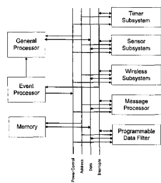
D e d ic a te d A r c h ite c tu r e for S en so r N e tw o r k A p p lic a tio n
Dedicated architecture for sensor network application is an event-processor-based architecture pro
posed by Harvard University [14] . It is intended to improve the power efficiency by fully leveraging
the event-driven nature of sensor network applications. The architecture is shown in Figure 2.4. This
architecture is different from the CPU-based embedded system in the way th a t events arc handled
by a dedicated event processor. The event processor is essentially a programmable state machine
to perform repetitive interrupt handling tasks. The hardware modules, such as message processor,
d ata filter, assist the event processor. These modules are designed for specific tasks. Therefore, they
improve power and cycle efficiency. The general purpose processor in the architecture is used as the
last resort for computation. It is used only when other modules do not have the requisite function.
Wireless sensor network are inherently event-driven [26]. Dedicated embedded systems use inter
rupts to indicate an event th at requires system’s attention. Therefore, the primary task of dedicated
embedded sensor node is to handle tim er and external interrupts [14]. A typical interrupt handling
procedure of an embedded system is as follows: W hen the occurrence of an event is detected, an
2. B A C K G R O U N D A N D P R E V IO U S W O R K
M emory Event P ro c e s s o r
G eneral P ro c e s s o r
Program m able Data Filter
Timer Su b sy stem
W ireless S ub sy stem
M e ssa g e P ro c esso r S e n so r S u bsy stem
Figure 2.4: Event-proeessor-based architecture
execution state and data. Then, the CPU loads corresponding event handling program from memory
and executes. After the execution is finished, the CPU has to restore its previous state and continue
the execution. The operations for embedded system to store and restore its execution state before
and after an interrupt is the overhead. The event driven architecture can avoid this overhead by
using dedicated event processor. The function event processor coordinates others hardware function
modules to respond to events. There is no software overhead for interrupt handling.
Since event-driven architecture avoids the overhead of running an operating system and interrupt
handling, the hardware designed for specific tasks improves the system performance. The cvcnt-
processor-based system[14] uses about 10 times less clock cycles th an dedicated embedded system.
The reduction of cycle count makes the event-processor-based architecture runs for less time at the
same clock frequency or enables it to run at a lower clock frequency and still execute a task in the
required time. The power consumption of a CMOS system is comprised of two parts, static power
consumption and dynamic power consumption. The dynamic power consumption is calculated by
2.1.
2. B A C K G R O U N D A N D P R E V IO U S W O R K
W here Pdyn is the total dynamic power consumption of the system, a is a measure of switching
activity, / is the clock frequency, C is the output capacitance of the node, and V is the power supply
voltage.
Running for less time or at a lower clock frequency reduces dynamic power and energy consump
tion. Another advantage of running at a lower clock frequency is th a t the processor can usually run
at a lower supply voltage, further reducing both dynamic and static power dissipation and energy
consumption.
2 .4
M o tiv a tio n o f O ur W ork
Dedicated architecture for sensor network applications can significantly improve performance of sen
sor system [14]. However, to our knowledge, there are still no sensor network applications developed
for dedicated architecture platforms. Lack of such platforms motivates us to implement a Zigbee
sensor node based on dedicated architecture to verify the system functionality and performance
using real-world applications.
The sensor node is based on an event-driven architecture. All system functions are implemented
using dedicated hardware modules. The dedicated hardware designed for specific tasks is more power
efficient than general purpose CPU for processing the same tasks [27]. Rabaey [1] compared energy
efficiency against flexibility among embedded processor, ASIC, FPGA and dedicated hardware.
As illustrated in Figure 2.5, the energy efficiency of dedicated hardware is about three orders of
magnitude higher than embedded processors.
Our design is targeted for implementation using FPGAs for flexibility, reasonably high speed, and
low cost. FPGA is very suitable for prototyping of sensor nodes because of its rc-programmability.
It is also an excellent platform for future design space exploration.
2. B A C K G R O U N D A N D P R E V IO U S W O R K
1000
?
0 100.S> % o 2 !E °
1*5 10
o
0.1
Dedicated HW
Reconfigurable
2V DSP: 3M OPS/m W
0.4 M IPS/mw
Flexibility (C overage)
C h ap ter 3
S y s te m A rchitecture
Wireless sensor networks are inherently event-driven[26]. All sensor node designs mentioned in
the previous chapter try to leverage the event-driven nature of sensor network applications to make
efficient use of resources. For example, TinyOS, the operating system for dedicated embedded sensor
system, has event-driven execution model; SNAP[13] has event-driven execution of instructions;
dedicated architecture for sensor network application in [14] has dedicated event processor. All these
research efforts suggest th a t energy efficiency can be obtained from optimizing the event handling
process. Our design also adopts specific event driven architecture to improve system performance.
The system architecture is illustrated in Figure 3.1. A Zigbee application is implemented using
six hardware units. The Zigbee application consist of three layers of communication: (1) physical
MAC layer(IEEE 802.15.4); (2) network layer(Zigbee) and (3) application layer. The hardware
units are cross-layer designed to minimize the communication among different layer functions. For
e x a m p le , p a r s in g a n d c la s s ific a tio n u n i t s p a n s a c r o s s t h r e e la y e rs. I t s i n p u t is in p h y s ic a l la y e r fra m e
while its output could be in MAC layer command or network layer command or application layer
3. S Y S T E M A R C H IT E C T U R E
buses. The dedicated links allows simultaneous communication among hardware units. The features
of our design are described in the following sections
Application Layer Application and
M an ag em en t Unit SlOW P ith ;[ ~
Z igbee Network
Control Unit Modification
an d Framing
Unit IEEE 802.15.4
R a d io C ontrol
Unit signal C C 2 4 2 0m odule Slow Path
Figure 3.1: The Zigbee implementation system block diagram
3 .1
E v e n t-D r iv e n A r c h ite c tu r e
All function units in our design are event-driven systems, except parsing and classification unit. The
general architecture of the event-driven system is shown in Figure 3.2. There are event handlers,
event dispatchers, data bus, control signals, and state signals in the architecture. Event dispatcher
is used to detect the occurrence of an event and activate the corresponding event handler to handle
th a t event. An event could be internal, such as timer signal, or external, such as packet available
in radio module buffer. Event handlers are dedicated hardware subsystems designed for specific
events. They are activated by an event dispatcher in response to a specific event. Event handlers
can generate other internal events. In this case, it activates another event handler to process the
internally generated events. An event handler consists of event processing unit, local registers and
shared registers. The event processing unit contains customized state machine and d ata path for
processing a particular event. The state machine controls the event processing. The data path
provides hardware needed for processing event information. Local registers are used for temporary
3. S Y S T E M A R C H IT E C T U R E
The shared registers are used for exchanging event information. Information from event dispatchers
is stored in shared registers. Both event handler and event dispatcher are able to access to the
shared registers. The control signal is used to trigger the event handler to change its state from idle
to active. The state signals indicate the state of event handlers to event dispatchers. The data bus
is used to transfer event information from event dispatcher/event handler to event handler. The
o utput ports in the architecture are driven by the event handlers, which are responsible for the
communication between hardware blocks.
C ontrol S ig n a ls & S tate S ig n als
Local R e g isters Jl
E vent H andler
O u tp u t
P o rts
S h a r e d R e g i s t e r s
D ata
Figure 3.2: Event driven architecture
An event dispatcher is a state machine designed to monitor the input ports of hardware blocks,
receive event information, decode event information and activate corresponding event handler. Fig
ure 3.3 illustrates a simplified version of the actual state machine of an event dispatcher. The event
dispatcher stay in Idle state after reset or power-on until an event occurs. W hen an event occurs,
event dispatcher receives event information from input port, decodes event information, and lookups
corresponding event handler to activate. If the event handler is in Idle state, the event dispatcher will
activate the event handler. The activation requires three steps. First, the event dispatcher signals
the event handler changing its state from Idle to JobAdd state. Then the event dispatcher receives
event information from input port and sends it to the shared registers of activated event handler.
Finally, after the information transaction is complete, the event dispatcher signals the event handler
3. S Y S T E M A R C H IT E C T U R E
the Idle state and continues to monitor the input interface. If the event handler is not in Idle state
when an event dispatcher has detected an event, the event dispatcher will hold the communication
on the input port and wait until the event handler is ready. Then the event dispatcher continues
th e activation as described above.
E v e n t h a n d le r n o t a v a ila b le
E v en t h a p p e n & ev e n t h an d ler n o t available
Wait
No Event .Event h an d ler available
Idle Activate
E v en t h a p p e n & E vent h an d ler av ailab le
Transferring Information
Transferring C o m p lete
T ran sfer
Figure 3.3: Event handler state machine
Each event handler is a small hardware processing unit with customized control logic and data
p ath to perform a specific task. Figure 3.4 illustrates a simplified version state machine of an actual
event handler. There are three common states in every event handler: (l)Idle, (2)JobAdd and
(■3) JobStart. All event handlers have same functionality in these states. The state change of event
handler from Idle to JobAdd, from JobAdd to JobStart is solely controlled by the activator, which
is cither the event dispatcher or the event handler th a t is activating this event handler. The event
handler stays in Idle after reset or power on. W hen in Idle state, the event handler is ready to accept
a task. Event handler is signaled to change from Idle to JobAdd state after the event dispatcher
has detected an event. The JobAdd state shows th a t the event handler is engaged to an event
handling and receiving event information. W hen in this state, the event information is transfercd
from event dispatcher to event handler’s shared registers. The event handler does nothing in this
state b u t waits until the transfer is complete. W hen the information transfer is complete, the event
dispatcher signals event handler to change its state from JobAdd to JobStart. From this state, the
3. S Y S T E M A R C H IT E C T U R E
event handler will return to the Idle state and wait for next event. Note th a t the event handlers
do not provide preemption operation and there is no priority to access a particular event handler.
They follow first-comc-fist-serve rule. W hen an event handler is busy, event dispatcher has to wait
until it is ready.
Inform ation is N o e v e n t tra n sfe rre d
E v e n t
T rig g er
Idle Jo b A d d (J o b S ta r tp {JobEnd Inform ation
tra n s fe r Is c o m p le te d
Figure 3.4: Event handler state machine
The operation of the designed system is driven by events. An event processing procedure consists
of three stages: (1) event detection, (2)handler activation, (3)evcnt processing. In event detection
phase, event dispatchers are in Idle state and monitor the input ports. W hen an event happens,
the event handler decodes event and begins handler activation phase. In handler activation phase,
event handler first checks the availability of corresponding event handler. If the corresponding event
handler is idle, event dispatcher transfers event information to the event handler. Otherwise, the
event dispatcher will wait until the event handler is ready. During this period, event handler is
in JobAdd state and event dispatcher in Activate state or Wait state. After the information is
transferred, the procedure enters event processing phase. The event dispatcher returns to idle state
and event handler starts the task processing. The whole event processing phase lasts until event
handler finishes its task. As described above, the event dispatcher is responsible for the event
detection and the event handler is responsible for event processing. Therefore, the event detection
phase and event processing phase could be overlapped. Also, because event handlers arc able to
work independently of each other, the event processing phases of different events can be overlapped,
making it possible to process events in parallel.
In our event driven system, all com putation resources needed for processing a particular event
3. S Y S T E M A R C H IT E C T U R E
to request the computational resources for processing the task. As a result, there is no interrupt
overhead in the our system.
3 .2
H a rd w a re A c c e le r a tio n
The most frequent tasks of a sensor node are sending a packet, receiving a packet and relaying
a packet. These activities involve operations such as parsing, classification, framing. In network
processors, these operations are accelerated in hardware using pipelining and parallel processing
[28] [29]. As shown in Figure 3.1, the designed system adopts the architectural ideas from network
processors to accelerate packet operations. There are two information paths in the designed system:
(1) fast path and (2) slow path. The function units in fast path deal with operations th a t are
directly performed on packets, such as header modification, parsing, classification, packet framing.
This p ath has customized data p ath for IEEE 802.15.4 frames and Zigbee packets. It guarantees th a t
the throughput of the designed system is able to keep up with the line speed. The slow processing
p ath deals with operations th a t arc related to network management and upper layer application,
such as routing protocol handling and routing table updates. In a network processor, those functions
arc implemented by the central processing units (CPUs). However, in our system, a set of specific
hardware modules, event handlers, replace CPUs to accelerate the task processing.
3 .3
P a r a lle l D is tr ib u te d C o m p u ta tio n
Our system has two parallel d ata paths, fast p ath and slow path. Inside hardware units, each event
handler and event dispatcher has its own data path and control logic. They also work in parallel.
The parallel architecture in our system increases the efficiency of message processing and the system
throughput. The computation capability is distributed among event handlers which enable the
system to respond an event whenever it occurs. Implementation and testing results in chapter 4
show th a t the parallel distributed com putation allows our system to respond faster to application
3. S Y S T E M A R C H IT E C T U R E
There is a trade-off between size of circuit and performance. The parallel distributed compu
tation architecture of our system has larger size circuit than other CPU-based architectures. In
our implementation, we did not encounter restrictions on circuit size. As shown by the synthesis
results in Chapter 4, our implementation uses about 51 percent of the target FPGA logic capacity.
There is still plenty of logic capacity left unused. For implementations with very tight circuit size
constraint, it is possible for the designed system to combine some event processing units into one
common processing unit to reduce circuit size.
3 .4
S y s te m C o m p o n e n ts
Before presenting the system components, a brief description of Zigbee nodes and their behavior
is provided here. There are three type of Zigbee nodes: (1) coordinator, (2) router, and (3) end
device. The coordinator is responsible for initiating and maintaining the network. It is the root of
the network and there is only one coordinator in a Zigbee network. Router is responsible for moving
data and control messages through the network. Router extends the coverage of the network. End
device contains just enough functionality to talk to coordinator or router; it cannot relay data from
other nodes. Both coordinator and router provide an association service for new node to join to
a network. Association is a procedure used to establish membership in a network. A parent-child
relationship is formed when a node having membership in the network allows a new node to join.
The new node becomes the child, while the other node becomes the parent. The parent will assign
a 16-bit network (NWK) address to its new children based on its capability. For router,the 16-bit
NWK address is calculated based on Equation 3.1; for end device, the function is determined by the
Equation 3.2:
3. S Y S T E M A R C H IT E C T U R E
Where
1 4- C — R — C * R Lm- d- 1
Cskip{d) = — - ---^ ^ ^ --- (3.3)
1 — R m
ARouter„ is the network address of n ih router’s child. A parent is the network address of the parent.
Cskip(d) essentially the size of the address sub-block being distributed by each parent at th a t depth
to its routcr-capable child node for a given network depth. It is given by Equation 3.3. Cm gives
the maximum number of children a parent may have. L m is the maximum depth of the network. It
specifies the maximum number of allowable levels in a particular network tree. R m is the maximum
number of routers th a t a parent may have as children.
The implementation in this thesis support Zigbee coordinator functions and router functions. As
shown in Figure 3.1, our system consists of parsing and classification unit, modification and framing
unit, network control unit, application and management unit, radio control unit and CC2420 unit.
System’s functional units are connected to each other by dedicated links. The functions of these
units are described below.
3 .4 .1
R a d io c o n tr o l u n it
Radio control unit interfaces to the CC2420 transceiver module to provide a communication channel
to other modules in the system. It provides three operations: (1) get-packet, (2) send-packct and
(3) TRX-configuration.
1. Get-packet: This operation is triggered when CC2420 module signals th a t there is a packet
available in its buffer. Get-packet operation gets packets from CC2420 buffer and sends the
packets to parsing and classification unit.
2. Send-packct: This operation is triggered when modification and framing unit sends a packet
to radio control unit. Radio c o n tr o l u n i t re c e iv e s the p a c k e t a n d s e n d s i t t o CC2420 m o d u le .
The whole send-packet operation consists of four steps. First, radio control unit will issue a
clear command to CC2420 module to clear its buffer. Then, radio control unit receives the
3. S Y S T E M A R C H IT E C T U R E
transfer is finished, radio control unit will issue a send command to CC2420 module. When
CC2420 receives this command, it changes from receive mode to TX mode. CC2420 will
sta rt to send the packet when the wireless channel is free. After sending the send command
to CC2420, radio control unit keeps monitoring the state of CC2420 module until CC2420
finishes sending. W hen the send packet operation is finished the radio control unit return to
idle state.
3. TRX-configuration: This operation is triggered when network control unit needs to command
or configure CC2420 module, or read CC2420 module state. When network control unit
sends command or configuration param eter to radio control unit, radio control unit will write
them to the corresponding CC2420 register. At the same time, radio control unit reads
CC2420 state and sends it back to network control unit. W hen network control unit reads
the content of CC2420 register, radio control unit will send read-register command and the
register address to CC2420 module. Then it receives the module’s states and the register’s
value from CC2420 and sends them to network control unit.
3 .4 .2
P a r sin g a n d c la s s ific a tio n u n it
Parsing and classification unit receive packets from radio control unit and parses the received packets
into information fields. The parsed information is then sent to corresponding module for further
processing based on the packet type. Some unnecessary information fields are removed. For example,
the MAC command is sent to network control unit and the application data are sent to application
and management unit. The destination MAC address is removed because it is not needed in further
processing. The Zigbee frame structure is shown in Figure 3.5 and the input frame and output data
format of parsing and classification unit are shown in Figure 3.6. The input frame types include
3. S Y S T E M A R C H IT E C T U R E
Bits:0-2 3 4 5 6 7-9 10-11 12-13 14-15
F ram e type
Security en a b le
F ram e pending
Ack. r e q u e s t
Intra-PAN R eserv ed
D est ad d ressing
m ode R eserved
S o u rce ad d ressin g
m ode
O ctets:2 1 0/2 0/2/8 0/2 0/2/8 variable 2
F ram e control
S e q u e n c e n u m b er
D estination PAN Identifier
D estination a d d r e s s
S o u rce PAN Identifier
S o u rce
a d d re s s F ram e playload FC S A d d ress fields
MHR MAC
playload MFR
Figure 3.5: Zigbee frame structure
1 4/16 i variable
Frame control Seq. Num. A ddress fields NWK Head e r Application h ead er
Application d ata play load NWK Data playload MAC D ata playioad
MHR MAC playload
NWK
Head NWK playload er
MAC data: NWK data: Application d ata
Octet&T-•1 4/10 6/8 1 variable
*■ NWK NWK NWK
Frame Seq. A ddress H eade Com m and Com m and
control Num. fields ID playioad
D ata playload
MHR MAC playload
MAC data: NWK com m and
O ctets:2 1 4/10 2 variable 2
F ram e control Seq. Num. A ddress fields Command ID
Com m and playioad FCS
MHR MAC playload MFR
MAC com m and
UUUIIU.
1 4/10 2 variable 2
F ram e control Seq. Num. A ddress fields S uper frame S pec Beacon playload FCS
MHR MAC playioad MFR
Source Addres Application
Data ID Data playload
o application and M anagem ent unit
NWK Command ID Source Addres Command ptayload To Framing and
modification unit
To network control unit
Command playload Command A ddres
S uper frame Spec Beacon playload S ource Addres Parsing and modification unit
To network control unit
3. S Y S T E M A R C H IT E C T U R E
3 .4 .3
N e tw o r k c o n tr o l u n it
Network control unit processes MAC layer and Zigbee network layer events. Its functions includes
network discovery, network start, network join , neighbor table maintenance, etc. It is also respon
sible for configuring CC2420 transceiver, and resetting MAC layer and physical layer.
Network control unit interfaces to parsing and classification unit, application and management
unit, modification and framing unit and radio control unit. In network control unit, There arc two
event dispatchers and fourteen event handlers. One event dispatcher monitors the interface between
parsing and classification unit; the other monitors the interface between application and management
unit. These two dispatchers work independently in parallel. The name of event handlers and their
functions are listed as follows.
1. send-ToFrame: This event handler is activated when an event handler needs to send
information to other nodes in the zigbee network. The process will send d ata to modification
and framing unit, where data are packed as a Zigbee frame.
2. send.ToNWK: This event handler is activated when an event handler need to send
information to application and management unit. This event handler is responsible for the
communication between network control unit, and application and management unit.
3. ToCC2420-process: This event handler is activated when an event handler needs to
command or configure CC2420 module. This event handler is responsible for communication
between network control unit and radio control unit.
4. bcacon.process: This process is activated when network control unit receive a beacon. It
compares the (personal area network Identifier) PAN ID in beacon with those in its neighbor
table. If the PAN ID in beacon is different from those in neighbor table and neighbor table
has still has capacity, it adds a new neighbor to its neighbor table and notifies application
and management unit th a t a new neighbor is found. Otherwise, it ignores the beacon. In
order to notify application and management unit, a new event process, scnd_ToNWK, will be
3. S Y S T E M A R C H IT E C T U R E
5. associate_req: This process is activated when network control unit receives the MAC
command, association request. It checks if the requesting nodes are already in children table.
If they arc, then event handler assigns the old 16-bit NWK address to the requesting node. If
the requesting node is not in children table, event handler will assign a new 16-bit NWK
address to the requesting node and adds new entity in children table. In both cases, the
association attem pt succeeds. If there is no capacity in children table, the association
attem pt fails. Event handler will send an association response command to tell the
requesting node the result of association attem pt. The association state and 16-bit NWK
address will be in th a t command. In order to send the association response command, the
send_ToFrame event handler will be activated at the end of this process.
6. associate.resp: This process is activated when network control unit receive the MAC
command frame of association response. If the node has already been associated with a
Zigbee network, event handler will ignore this event. If the association response is with a
success state, the event handler will setup 16-bit network address and PAN ID based on the
information from association response command. It also activates ToCC2420_proccss event
handler to configure CC2420 module, and activates send-ToNWK event handler to inform
application and management unit th a t association with a Zigbee Network is successful. If the
association response returns w ith a failure state, the event handler informs application and
management unit th a t the association attem pt failed.
7. beacomrcq: This process is activated when network control unit receives a search for Zigbee
network request from application and management unit. The event handler will construct a
beacon request command and activate send.ToFramc event handler to send the command.
8. join-nctwork: This event handler is activated when network control unit receives a join to a
network command from application and management unit. The event handler will first
lookup neighbor table to found a suitable Zigbee network to join. If no Zigbee network
found, event handler will send a message back to application and management unit to inform
3. S Y S T E M A R C H IT E C T U R E
association request command to the network. The send.ToFrame event handler will be
activated to send the Zigbee frame.
9. search_network: This event handler is activated when network control unit receive a search
network command from application and management unit. A beacon request command will
be constructed and broadcasted. The send.ToFrame event handler will be activated to send
the Zigbee command.
10. send.NW Kdata: This event handler is activated when network control unit receive a data
package from application and management unit. Event handler constructs a Zigbee data
frame. Frame length, frame control field, PAN ID, sequence number and source address arc
added to the frame. Then event handler activates the send.ToFrame event handler to send
the frame.
11. initial.CC2420: This event handler is activated after sensor node is powered up or reset. The
event handler sets up PAN ID, 64-bit IEEE address, 16-bit network address, frequency and
buffer size in CC2420 module, It also turns on the crystal oscillator in CC2420 module and
sets CC2420 in receive mode.
12. start-NW K: This event handler is activated when network control unit receive a start
network command from application and management unit. Event handler sets up sensor
node to be a Zigbee coordinator.
3 .4 .4
A p p lic a tio n a n d m a n a g e m e n t u n it
Application and management unit interfaces to parsing and classification unit, network control
unit, modification and framing unite. It has network management, application function and user
interface function. The network management controls the process of setup and joining a Zigbee
network and routing. Application function controls a test application. The test application mimics
data monitoring scenario in real-world Zigbee application. User interface controls the output of
3. S Y S T E M A R C H IT E C T U R E
3 .4 .5
M o d ific a tio n a n d fra m in g u n ite
Modification and framing unit is responsible for packing the data into frames th a t will be sent to
other Zigbee nodes. It interfaces with parsing and classification unit, network control unit, radio
control unit. It consists of a dispatcher and two event handlers. The dispatcher monitors the events
at its two interfaces. If a packet is received from parsing and classification unit, event handler starts
route lookup process. The route lookup process sends a request to application and management unit
for ncxt-hop address. The return address will be framed in the packet. For packets from network
control unit, event handler adds MAC source address and sequential number. The frame is then
transferred to radio control unit.
3 .4 .6
C C 2 4 2 0 m o d u le
CC2420 module is the low power, IEEE 802.15.4 [8] and ZigBee compatible, RF chip CC2420 [30].
It is used as a wireless transceiver. The description and functionality of this chip are presented in
![Figure 2.5: Analysis of energy efficiency versus flexibility trade-off for a number of common architectural styles (for a 0.25 micron CMOS process)[1].](https://thumb-us.123doks.com/thumbv2/123dok_us/1472999.1180390/29.617.215.446.311.464/figure-analysis-energy-efficiency-versus-flexibility-tectural-process.webp)