binding energies between the peaks due to the substrate Si and the oxide SiO2. Recently we have shown that significant interface changes with annealing for the SiO2/Si system commonly used for FET gate dielectrics illustrating the effectiveness of SXPS for the current study. The present article presents SXPS studies using synchrotron radiation of the electronic structure at the interface between Ta2O5– Al2O3 alloys and Si共111兲. This system is typical of FET alternative-gate-oxide films and has an electronic structure characteristic of high-k gate dielectrics. Thin films (⬍20 Å) of Ta2O5– Al2O3 alloys were carefully prepared using remote plasma enhanced chemical vapor deposition on Si共111兲. For this study, SXPS spectra were taken for the Si 2 p, Al 2 p, and Ta 4 f core levels. The Si 2 p SXPS data confirm that SiO2is formed at the Si interface during deposition for all alloys 共in agreement with previously published results兲 and that the Si interface is qualitatively similar to SiO2/Si samples. The binding energy of the Si4⫹ Si 2 p3/2 core level varies significantly for our alloy samples and this is interpreted as a screening effect rather than being due to Ta or Al silicate formation. The Al 2 p and Ta 4 f SXPS core level peak positions reveal screening effects. For these data, line shape analysis also supports alloy homogeneity as independently determined by Auger electron spectroscopy and Fourier transform infrared spectroscopy. © 2002 American
Vacuum Society. 关DOI: 10.1116/1.1493786兴
I. INTRODUCTION
Alternative dielectrics are being considered as replace-ments for the standard SiO2 gate oxide in metal–oxide– semiconductor field-effect transistor 共MOSFET兲 devices. Present strategy plans for a gate dielectric material with a dielectric constant higher than SiO2that can be used to avoid difficulties with ultrathin (⬍20 Å) SiO2 gate dielectrics, such as high leakage current and reliability.1Such a material must satisfy a narrow set of requirements to be effective. One of these requirements is a high-quality interface with Si; another requirement is low interface states at the Si interface to reduce MOSFET channel mobility and trap charge. These potential problems can be alleviated with the presence of an intermediary SiO2layer; however, such an intermediate layer greatly reduces the effectiveness of the alternative dielectric. It is also imperative that the dielectric and interface be stable during deposition or growth and post-processing.
Soft x-ray photoelectron spectroscopy共SXPS兲using syn-chrotron radiation is an effective tool for characterizing an interface with silicon. The SiO2/Si interface has been stud-ied in detail with SXPS by various authors.2– 8These previ-ous studies have shown that SXPS examination of the Si 2 p core level for ultrathin films of SiO2on Si reveals five states: bulk Si, three interface suboxide states, and the SiO2, la-beled Si0, Si1⫹, Si2⫹, Si3⫹, and Si4⫹, respectively, referring to the oxidation state of silicon. Though this simple, common
interpretation2,3,6,9has been a subject of controversy,4,5,8,10it is supported by the latest investigation into the matter.11 Fig-ure 1 shows the raw Si 2 p SXPS data共a兲for less than 10 Å of SiO2on Si共111兲and the spin–orbit stripped data共b兲 show-ing only the Si 2p3/2 component. The 0.602 eV spin–orbit splitting of the substrate 2p core level is clearly seen in the raw data and illustrates the resolution (⬍0.1 eV) of SXPS. Previously, it has been determined that the relative intensities of the specific interfacial suboxide peaks depend not only on the oxide and interface quality, but also on characteristics such as annealing temperature,8crystal orientation,2 nitrida-tion level,8and vicinal cut.9,12
In this study, SXPS of the Si 2 p3/2 core level is used to characterize the interface between the pseudobinary (Ta2O5)x(Al2O3)1⫺x alloys and Si共111兲. Spectra for the
maximum shifts are several times larger in the AES spectra than in the SXPS spectra. A small shift in the SXPS peak positions is observed and is consistent with the small differ-ence in electronegativity of the end-member oxides. The AES measurements indicate that the metal oxides are sepa-rated from the Si substrate by approximately 5–10 Å of SiO2, and SXPS studies of the Si 2 p core level verify the presence of a SiO2 layer. Both the increased Gaussian width and energy shift of the Si4⫹ peak together have been typi-cally interpreted as due to the presence of interfacial silicate layers.13,14However, in this article we point out an alterna-tive interpretation that involves screening of the core hole by both the surrounding oxide-layer atoms and the proximity of both the Si substrate and the high-k overlayer dielectric.
II. EXPERIMENTAL DETAILS AND RESULTS
A. Sample preparation
Hydrogen terminated Si共111兲substrates were prepared by growing a thermal oxide, subsequently etching the majority of this oxide with 共50:1兲 HF, and removing the final oxide using 40% NH4F. Thin films of the Al2O3, Ta2O5, and their alloys were deposited by remote plasma enhanced chemical vapor deposition共RPECVD兲15 using triethyldialuminum tri-sec-butoxide共TEDA-TSB兲and tantalum pentaethoxide共 TA-ETO兲as a source of aluminum and tantalum, respectively. A schematic of the process chamber is provided in Fig. 2. The H-terminated substrates were placed on the sample mount and heated in vacuum to 300 °C. Helium carrier gas was bubbled through the liquid metal organic sources. The partial
pressure of the metal organic was controlled by the tempera-ture of the source and total pressure over the source. The TEDA-TSB and TAETO sources were held at 74.4 and 114.3 °C, respectively, while the total pressure over each source was chosen between 30 and 200 Torr depending on the desired alloy composition. These species were introduced into the process chamber via the He carrier gas through the injectors at 20 sccm each. He and O2 were supplied sepa-rately to the process chamber at 200 and 20 sccm, respec-tively, and excited with a 13.56 MHz radio frequency plasma power source of 30 W. The process chamber pressure was maintained at 0.3 Torr. Deposition was for 15 s. Three alloy compositions, an Al2O3end member and a Ta2O5 end mem-ber were deposited. In a later experiment, a second Al2O3 sample with a deposition time of 10 s was prepared. Alloy composition was determined by comparing Al and Ta peak intensities from on-line AES which had been previously cali-brated against Rutherford backscattering spectrometry 共RBS兲. The Ta2O5 composition of the three alloys were de-termined to be 34%, 43%, and 74%. Each sample was sub-sequently annealed by rapid thermal annealing共RTA兲for 30 s. The Al2O3 samples and 74% Ta2O5 sample were annealed at 800 °C, the 34% and 43% Ta2O5 samples at 900 °C, and the Ta2O5 sample at 700 °C. These temperatures were cho-sen to be less than the temperature necessary to cause crys-tallization of the oxide.16
For reference and comparison, a thin film of SiO2 on Si共111兲was prepared by plasma enhanced oxidation using a similar process. This sample was exposed to 200 sccm of He and 20 sccm of O2with the same plasma conditions for 30 s and annealed at 900 °C by RTA for 30 s.
B. SXPS measurements
Samples were transported from the RPECVD process chamber at North Carolina State University to the U4A beamline of the National Synchrotron Light Source 共NSLS兲 in a nitrogen atmosphere to minimize exposure to air. The FIG. 1. Soft x-ray photoemission spectroscopy results:共a兲raw Si 2 p SXPS
data and共b兲spin–orbit stripped data (Si 2 p3/2) of ultrathin共⬍10 Å兲SiO2on Si共111兲indicating spin–orbit splitting together with interpretation of peaks.
FIG. 2. Schematic diagram of the film growth chamber using the remote plasma enhanced chemical vapor deposition process.共a兲The gases He and O2are introduced and excited with a rf power source.共b兲 Triethyldialumi-num tri-sec-butoxide and tantalum pentaethoxide sources are introduced through共c兲the injectors.共d兲Sample mount.
samples were exposed to air for several hours during re-moval from the RPECVD chamber and during mounting and transfer into the SXPS vacuum chamber. The SXPS configu-ration at the U4A beamline includes a 6 m spherical grating monochromator producing photons between 20 and 250 eV with a resolution on the order of 0.1 eV. Photoelectron ki-netic energy is measured with a VSW 100 mm hemispherical analyzer fixed at 45° relative to the photon beam axis. Mea-surements were taken at normal takeoff.
The Si 2 p3/2 binding energy of the bulk silicon substrate measured from the top of the valence band was 98.8 eV. This is essentially the same as 98.75 eV as reported by Himpsel
et al.17The Si 2 p3/2 binding energy of the substrate with re-spect to the Fermi level was 99.8 eV and was used as an energy reference for Figs. 3–5. The Si 2 p3/2 SXPS single-component spectra used in most of the plots in this article were extracted from the raw data by using a standard spin– orbit stripping procedure2with a spin–orbit energy splitting of 0.602 eV and a branching ratio of 2:1 共see Fig. 1兲. The resulting Si 2 p3/2 spectra were fit using five Voigt peaks. In the case of the alloy samples, a satisfactory fit was obtained with only four Voigt peaks. Typical Voigt function model peaks were used with a Lorentzian width at half-maximum fixed at 80 meV and a variable Gaussian width to simulate the experimental data. The unstripped Al 2 p SXPS data were fit using a pair of Voigt peaks with a fixed spin– orbit splitting of 0.45 eV and branching ratio of 2:1. The unstripped Ta 4 f SXPS data were fit with a pair of Voigt peaks without fixing the splitting or branching ratio. Best fits of both stripped and unstripped data were determined using a nonlinear least squares algorithm that has been described
previously.18,19The ‘‘best-fit’’ peaks were dominated by the Gaussian component which represents the quadrature sum of the instrumental width, phonon broadening, and inhomoge-neous disorder in the sample.
III. RESULTS
A. SXPS and AES experiments
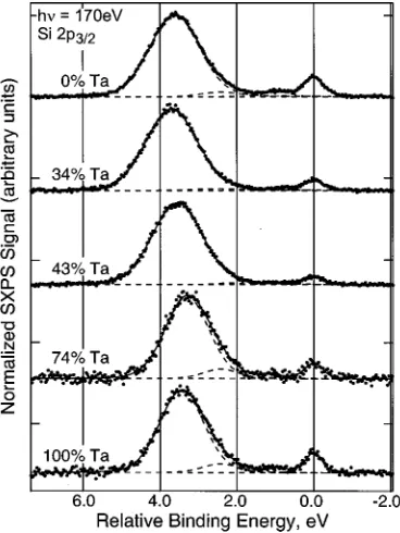
Figure 3 compares the Si 2 p3/2 SXPS spectra for the Al2O3 and Ta2O5 end members with that for the SiO2 sample. Note the similarity of the SiO2/Si interface peaks 共see Fig. 1兲 relative to the Si0 substrate peak for all three spectra. Figure 4 shows the Si 2 p3/2 SXPS spectra for the (Ta2O5)x(Al2O3)1⫺xalloys and the end members. The Si4⫹
peak is present in all samples, however its position and width are variable. This peak has a binding energy which varies for different samples and is between 0.2 and 0.5 eV lower than for the Si4⫹ peak of the SiO2 sample. Suboxide states are also present although more difficult to resolve. The Si sub-oxide states detected in these high-k samples were generally broader than for pure SiO2/Si interface peaks and acceptable fits to the spectra were obtained using two instead of three peaks to represent them.
Figure 5 shows the Al 2 p and Ta 4 f SXPS data for the (Ta2O5)x(Al2O3)1⫺x films. Panel 共a兲 shows the fitted data
for the Al 2 p core level of the Al2O3 sample indicating an assumed spin–orbit splitting of 0.45 eV and a branching ra-tio of 2:1. The two peaks are unresolvable and the spin–orbit splitting and branching ratio were fixed during fitting. Excel-lent fits were obtained with a pair of Voigt functions. The binding energy of the Al 2 p for the Al2O3 film is 75.9 eV, which is 1.2 eV larger than the reported value of 74.7 eV for bulk Al2O3.
20
Panel共b兲of Fig. 5 shows the Al 2 p3/2 single-FIG. 3. Comparison of Si 2 p3/2SXPS data for Ta2O5and Al2O3on Si共111兲
with SiO2on Si共111兲. The data are normalized to the Si
4⫹peak height.
component spectra for the Al2O3 sample and the three alloy samples. As the Ta composition is increased, the binding energy decreases linearly 0.6 eV. Panel 共c兲 of Fig. 5 shows the fitted data for the Ta 4 f core level of the Ta2O5 sample. Neither the spin–orbit splitting nor the branching ratio were fixed during fitting. The spin–orbit splitting was determined to be 1.92 eV which is 7% larger than the reported value.20 The branching ratio was 10:7 and this is also 7% larger than the theoretical ratio of 4:3. The binding energy of the Ta 4 f core level for our Ta2O5 film is 27.4 eV, which is 1.0 eV larger than the reported value of 26.4 eV for bulk Ta2O5.20 Panel 共d兲 of Fig. 5 shows the Ta 4 f7/2 single-component spectra of the Ta2O5 and three alloys. The binding energy also decreases linearly with increasing Ta composition, how-ever only by 0.2 eV.
In addition to the SXPS results described above, we also separately studied the oxides with in situ AES. The interface formation for the Al2O3end member was investigated during the initial stages of film deposition by interrupting the depo-sition process every 10 s and taking AES data.21,22The spec-trum revealed two silicon peaks, one for silicon bonded to silicon, 共Si–Si兲, at 91 eV and another of silicon bonded to oxygen,共Si–O兲, at 76 eV. The ratio of the two is consistent with approximately 6 Å of SiO2 being formed at the
inter-face during the initial stages of deposition.21,22For the Al2O3 end member, the layer of SiO2 is not increased in thickness for longer deposition times and is not changed during post-deposition annealing. These results are consistent with nuclear reaction analysis 共NRA兲, and capacitance–voltage measurement techniques.21 The AES data for a set of Ta2O5– Al2O3alloy samples is shown in Fig. 6. Two dashed lines are provided to indicate the 共Al–O兲and 共Ta–O兲peak positions for the end members. As the Ta composition in-creases, both the 共Al–O兲and共Ta–O兲peaks shift linearly to higher energy. The 共Al–O兲 peak shifts 2.0 eV and the 共Ta–O兲 peak shifts 3.0 eV. Figure 7 summarizes the Al 共a兲 and Ta共b兲peak shifts as a function of Ta2O5composition for both SXPS and AES.
B. Supporting device results
Films of (Ta2O5)x(Al2O3)1⫺xdeposited by the RPECVD
procedure described above have been further characterized by Fourier transform infrared spectroscopy共FTIR兲, confirm-ing that the alloys are homogeneous and pseudobinary.16 Both FTIR and AES studies indicate that the infrared active vibrational modes and electronic states of the alloys are not simply a superposition of the end-member compounds, but FIG. 5. Series of SXPS curves for共a兲 Al 2 p data for the Al2O3 sample;共b兲 Al 2 p3/2single-component spectra for the Al2O3 sample and three alloy samples;共c兲Ta 4 f SXPS data for the Ta2O5sample; and共d兲Ta 4 f7/2 single-component spectra for the Ta2O5 sample and three alloy samples. The term BR refers to the spin–orbit inten-sity branching ratio.
rather display features indicative of new bonding arrange-ments that are expected in a homogeneous pseudobinary al-loy. Changes in the FTIR spectra as a function of annealing further indicate the crystallization temperature of the alloys is increased with respect to the end-member crystallization temperatures by approximately 100 °C. For Al-rich alloys, this temperature increases from 900 °C for Al2O3, to 1000 °C and for Ta-rich alloys from 800 °C for Ta2O5, to 900 °C.
The electrical properties of (Ta2O5)x(Al2O3)1⫺x alloys have been investigated using capacitance–voltage (C – V) and current density–voltage (J – V) measurements as a func-tion of temperature. The alloys display significant flat band shifts to more positive voltages and additionally significant hysteresis. The positive increase in flat band voltage can be attributed to negative charge at the interface with or in the bulk oxide. The dependence of flat band voltage on thickness has been used to determine the location of this charge. For Al2O3 devices there is a linear dependence on thickness in-dicating that fixed charge is located at the interface between the Al2O3 film and the interfacial SiO2 layer.21This assign-ment is based on the temperature dependent C – V and J – V traces, where the absence of significant hysteresis indicates that the dominant contribution to the positive flat band volt-age shifts are due to fixed not trapped charge. The flat band dependence has not been investigated for the alloys, but the shift to positive values is larger and includes significant hys-teresis as well. This is consistent with increased negative charge that is due to trapping of electrons as well as fixed charge. The direction of the hysteresis is consistent with electron trapping in the oxide in the immediate vicinity of the interface. The temperature dependent measurements have
revealed the presence of two traps: 共i兲an interface trap 0.3 eV above the Si conduction band edge due to the Ta d states; 共ii兲a bulk oxide trap 1.4 eV above the Si conduction band edge.16
IV. DISCUSSION
The Si4⫹ peak present in all samples of this study 共see Figs. 3 and 4兲 indicates that a significant layer of SiO2 has formed between the deposited dielectric and the substrate. This is in agreement with AES studies of Al2O3 and Ta2O5 deposited by the RPECVD technique described above which show that roughly 6 Å of SiO2forms at the interface during deposition.21,22 The binding energies of the two interface peaks in the Si 2 p3/2 SXPS spectra共see Figs. 3 and 4兲give good indication that they correspond to the suboxide states Si1⫹ and Si3⫹. It is more difficult to resolve the Si 2 p sub-oxide states for the (Ta2O5)x(Al2O3)1⫺x films 共compare
Figs. 3 and 4 with Fig. 1兲because of signal attenuation due to the high-k and SiO2 layers. Because the Si2⫹ state was unresolvable in these films and only a qualitative analysis of the interface was desired, a peak was not assigned to this state in the fitting process. It is assumed that the Si2⫹ sub-oxide state is also present but perhaps weaker and therefore unresolved. In support of this, the Si2⫹ suboxide state is reported2 to be the least significant in the annealed SiO2/Si(111) interface.
It should be noted that the presence of silicate might also explain the variations in the Si4⫹ peak positions shown in Figs. 3 and 4. Differences in chemical shifts between SiO2 and silicates are small enough to make it improbable that FIG. 7. Plot of AES and SXPS shifts for共a兲Al 2 p3/2and共b兲Ta 4 f7/2core levels for (Ta2O5)x(Al2O3)1⫺xalloys as a function of alloy composition x. The lines are provided as a guide to the eye.
SXPS could distinguish them. Thus, the Si4⫹peak could be originating in part or in whole from a silicate. Deposition techniques other than RPECVD have been shown to form a silicate layer for both Al2O3共Ref. 13兲and Ta2O5.
23
Previous studies have used NRA to analyze Al2O3deposited using the RPECVD procedure used in this study and have shown that the interface between the Al and Si species is abrupt.21Thus the presence of any silicate is limited to the narrow region of an Al2O3/SiO2interface. In this case, the SiO2signal would dominate the silicate signal. Similar data do not exist for Ta2O5 deposited by RPECVD. In light of the NRA results discussed above, the Si4⫹ peaks in Figs. 3 and 4 are inter-preted as SiO2. Profiling techniques such as NRA or medium energy ion scattering are necessary before a definitive con-clusion can be reached.
The variable Si4⫹ Si 2 p3/2peak position共which has sys-tematically smaller binding energy compared to the SiO2/Si sample兲for our alloy samples is attributed to differences in film thickness and core hole screening due to the close prox-imity of materials with different dielectric constants.8 The binding energy of a photoelectron from an ultrathin film is affected by the substrate screening the core hole. The high-frequency dielectric constants of Si and SiO2 are 11.8共Ref. 24兲 and 2.1 共Ref. 25兲, respectively. The high-frequency di-electric constants of Al2O3 and Ta2O5 共which can be ob-tained from the index of refraction which are, respectively, reported26to be 1.67 and 2.23兲are 2.8 and 5.0, respectively. For SiO2 films on Si, the Si4⫹binding energy decreases with decreasing film thickness8,27–30and this variation is well de-scribed by an image charge model for the core hole screening.8 As the SiO2 film thickness decreases, the core hole screening increases due to the closer proximity of the substrate causing a decrease in the Si4⫹ binding energy. Likewise, if the SiO2is adjacent to a material such as Al2O3 instead of vacuum, screening is greater and the Si4⫹binding energy is less. This is in qualitative agreement with the dif-ferences in binding energies revealed in Figs. 3 and 4. More detailed discussion of these effects for other transition-metal oxide systems on Si substrates will be presented in a future publication.
The Al 2 p and Ta 4 f data shown in Fig. 5 provides infor-mation about the film quality and substrate interactions in the photoemission measurement. For each data curve the SXPS spectral line shape is well fit with a single spin–orbit split Voigt function pair. This indicates that there are no resolved Al or Ta suboxides in the metal oxide film. Our result is in agreement with information from Auger data taken on Al2O3 and Ta2O5 samples.
21,22
The increased binding energy of each end member over the reported binding energy20 is in-terpreted as due to core-hole screening in the high-k film as expected. Because SiO2 has a lower high-frequency dielec-tric constant than the high-k film, core-hole screening in the high-k film is reduced and the binding energy is increased by the presence of the underlying SiO2 film.
There is also a shift of the binding energy of the Al 2 p3/2 and Ta 4 f7/2 peaks with alloy composition as can be seen in Fig. 5, panels 共b兲 and共d兲. The data in Fig. 6 show similar
peak shifts for the AES data. These shifts for AES and SXPS are summarized in Fig. 7 which shows the binding energy shift versus alloy composition for both types of peaks. Lower resolution and complex line shapes contribute to the uncer-tainty in the AES data. Because the AES measurement has a two-hole final state in the valence band, the larger AES shifts are attributed to a change in the bonding environment with O nearest-neighbor atoms as Al atoms are replaced with Ta atoms. The SXPS measurement has only a one-hole final state in the core level and thus in principle should be more straightforward than the AES data to interpret. A change in the bonding environment with O would produce a SXPS peak shift that is smaller than for the AES data by a factor of 4 consistent with the square of the charge states of the two measurements. However, the detailed interpretation of the SXPS peak shifts is more complicated since core hole screening is expected to also play a role. The simple square-law dependence seems to work quite well for the Al 2 p peak shifts but does not seem to work for the Ta 4 f peak shifts.
In addition one must consider the sign of the peak shift. Electronegativity differences suggest that the average M–O bond 共M is Al or Ta兲 becomes slightly more ionic with in-creasing Ta concentration even though the Al–O near-neighbor coordination is expected to remain the same as the end-member Al2O3. Thus the increased Al 2 p binding en-ergy with increasing Ta concentration follows the initial state trend of more ionic bonding giving larger binding energy. However, this average bonding trend implies that a simple near-neighbor atom picture is not correct because the Al–O near-neighbor coordination does not change. Thus we con-clude that the SXPS shifts correspond to both near-neighbor and higher neighbor effects and the sign seems to follow the trend of more ionic bonding for increasing Ta composition. This is consist for both Al 2 p and Ta 4 f core levels since the sign of the shift is the same for the two levels.
We now consider the effect of core hole screening on the peak shifts. As the Ta composition is increased, the high-frequency dielectric constant is increased, causing the core hole screening to be increased and the photoelectron binding energy to be reduced. Since this effect combines with the chemical shift effect, it is difficult to assess the relative im-portance of these two effects. However, it appears that core hole screening contributes less significantly to the overall magnitude of the shift in the SXPS binding energies for the Ta 4 f core level than for the Al 2 p core level since the mag-nitude of the total shift is smaller for the Ta 4 f core level than for the Al 2 p level. The screening interpretation quali-tatively suggests a similar effect for both Al and Ta core levels and it is not apparent that one should observe differ-ences in these two core levels. Thus one must explain the complication that the Ta core level shifts less than the Al core level. The Ta 4 f core level has a binding energy of about 27 eV and is closer to the valence levels than the Al 2 p core level which has a binding energy of about 76 eV. In addition, the Ta 4 f core level has a more extended spatial distance from the atomic core center due to the orthogonalization of its wave function to those of the deeper core levels. We
We have studied the Si 2 p, Al 2 p, and Ta 4 f core levels using SXPS for the (Ta2O5)x(Al2O3)1⫺xalloy family of
ox-ides. The quantitative analysis of our Si 2 p SXPS data indi-cates that a 5–10 Å layer of SiO2 is formed at the interface 共an interlayer兲in agreement with previous AES studies. Dif-ferences in alloy–film interlayer Si4⫹binding energy are in-terpreted as resulting mainly from core hole screening rather than the presence of silicate composition mixing. This result has not been investigated before and is one of our main con-tributions. The analysis 共by least-squares methods兲 of Al 2 p3/2 and Ta 4 f7/2 SXPS data indicate that no Al or Ta suboxides are formed in the film. This is our most important result and it implies that there is no suboxide transition re-gion between the SiO2 and Al2O3 or Ta2O5 layers. Differ-ences between the Al 2 p of Al2O3 and Ta 4 f of Ta2O5 samples and published binding energies are attributed to core hole screening effects. The binding energy shifts in the SXPS Al 2 p and Ta 4 f core levels and AES 共Al–O兲 and 共Ta–O兲 peaks with alloy composition have been attributed to the combination of differences in the bonding environment and core hole screening.
ACKNOWLEDGMENTS
This work was supported by ONR, ARO, DOE, AFOSR, SRC, the SEMATECH/SRC Front End Process Center, and the NRC.
1G. D. Wilk, R. M. Wallace, and J. M. Anthony, J. Appl. Phys. 89, 5243
共2001兲.
2F. J. Himpsel, F. R. McFreely, A. Taleb-Ibrahimi, J. A. Yarmoff, and G.
Hollinger, Phys. Rev. B 38, 6084共1988兲.
3Z. H. Lu, M. J. Graham, D. T. Jiang, and K. H. Tan, Appl. Phys. Lett. 63,
2941共1993兲.
4M. M. Banaszak Holl, S. Lee, and F. R. McFeely, Appl. Phys. Lett. 65,
1097共1994兲.
5
K. Z. Zhang, M. M. Banaszak Holl, J. E. Bender IV, S. Lee, and F. R.
McFeely, Phys. Rev. B 54, 7686共1996兲.
and Chemistry of Semiconductor Interfaces, 7–11 January 2001共
unpub-lished兲.
13T. M. Klein, D. Niu, W. S. Epling, W. Li, D. M. Maher, C. C. Hobbs, R.
I. Hegde, I. J. R. Baumvol, and G. N. Parsons, Appl. Phys. Lett. 75, 4001
共1999兲.
14X. Zhao, M. Leavy, N. P. Magtoto, and J. A. Kelber, Appl. Phys. Lett. 79,
3479共2001兲.
15G. Lucovsky, D. V. Tsu, R. A. Rudder, and R. J. Markunas, in Thin Film
Processes II, edited by J. L. Vossen and W. Kern共Academic, New York, 1991兲, pp. 565– 619.
16R. S. Johnson, J. G. Hong, and G. Lucovsky, J. Vac. Sci. Technol. B 19,
1606共2001兲.
17F. J. Himpsel, B. S. Meyerson, F. R. Mc Feely, J. F. Morar, A.
Taleb-Ibrahimi, and J. A. Yarmoff, Core Level Spectroscopy at Silicon Surfaces and Interfaces, Proceedings of the Enrico Fermi School on Photoemis-sion and Absorption Spectroscopy of Solids and Interfaces with Synchro-tron Radiation, edited by M. Campagna and R. Rosei共North Holland,
Amsterdam, 1990兲, p. 203.
18G. K. Wertheim, J. Electron Spectrosc. Relat. Phenom. 60, 237共1992兲.
19G. K. Wertheim and S. B. Dicenzo, J. Electron Spectrosc. Relat. Phenom.
37, 57共1985兲.
20
C. D. Wagner, W. M. Riggs, L. E. Davis, J. F. Moulder, and G. E.
Muilen-berg, Handbook of X-Ray Photoelectron Spectroscopy 共Perkin–Elmer,
Eden Prairie, MN, 1979兲, pp. 50 and 144.
21R. S. Johnson, G. Lucovsky, and I. Baumvol, J. Vac. Sci. Technol. A 19,
1353共2001兲.
22
R. S. Johnson, Ph.D. thesis, North Carolina State University, Raleigh, NC, 2001.
23G. B. Alers, D. J. Werder, Y. Chabal, H. C. Lu, E. P. Gusev, E. Garfunkel,
T. Gastafsson, and R. S. Urdahl, Appl. Phys. Lett. 73, 1517共1998兲.
24D. F. Edwards, in Handbook of Optical Constants of Solids, edited by E.
D. Palik共Academic, Orlando, 1985兲, p. 566.
25H. R. Philipp, in Handbook of Optical Constants of Solids, edited by E.
D. Palik共Academic, Orlando, 1985兲, p. 760.
26H. Kattelus, M. Ylilammi, J. Saarilahti, J. Antson, and S. Lindfors, Thin
Solid Films 225, 296共1993兲.
27
S. I. Raider and R. Flitsch, IBM J. Res. Dev. 22, 294共1978兲.
28
F. J. Grunthaner, P. J. Grunthaner, R. P. Vasquez, B. F. Lewis, and J. Maserjian, Phys. Rev. Lett. 43, 1683共1979兲.
29G. Hollinger, Appl. Surf. Sci. 8, 318共1981兲.
30Y. Tao, Z. H. Lu, M. J. Graham, and S. P. Tay, J. Vac. Sci. Technol. B 12,