High Efficiency Flash ADC Using High Speed
Low Power Double Tail Comparator
Sruthi James
1, Ancy Joy
2, Dr.K.T Mathew
3PG Student [VLSI], Dept. of ECE, Viswajyothy College Of Engineering & Technology, Vazhakulam ,Kerala, India1
PG Student [VLSI], Dept. of ECE, Viswajyothy College Of Engineering & Technology, Vazhakulam ,Kerala, India2
Professor, Dept. of ECE, Viswajyothy College Of Engineering & Technology, Vazhakulam , Kerala, India3
ABSTRACT:Most of the signals in nature are in analog form. Processing of these analog signals is very difficult and effect of noise will be more. So we use ADC for converting Analog signals to Digital signals. For high speed application, Flash ADC is commonly used. In Flash ADC designs, the speed of thermometer to binary encoder often becomes the bottleneck in achieving high speed. In this work, a unique encoder is presented which exploits the signal pattern in the thermometer code and generates corresponding code which is converted then into equivalent binary bits. Comparator is another basic block of analog-to-digital converters (ADCs). High speed ADCs, such as flash ADCs, require high-speed, low power comparators. The need for ultra low-power, area efficient and high speed analog-to-digital converters is pushing toward the use of dynamic regenerative comparators to maximize speed and power efficiency. Four structures of comparators namely conventional dynamic comparator, conventional double-tail dynamic comparator, high speed dynamic comparator and high speed low power dynamic comparator were analyzed. In high speed low power dynamic double-tail comparator, both the power consumption and delay time are significantly less when compared to other comparators.
KEYWORDS: ADC, comparator, encoder.
I.INTRODUCTION
The signals in the real world are analog in nature. In order to achieve digital signal, we need to convert the analog signal into digital form by using a circuit called analog-to-digital converter. Whenever we need the analog signal back, digital-to-analog converter is required. Analog to digital converters are vital to many modern systems that require the integration of analog signals with digital systems. The applications of digital system can range from audio to communications applications to medical applications. These converters are implemented using a variety of architectures, sizes and speeds. The demand for the converter is oriented on area, speed, power of the converters. This has led to the investigation of alternative ADC design techniques.
Analog-to-digital converters (ADCs) are used to convert real world analog signals into digital representations of those signals. The digital signal processing can then efficiently extract information from the signals. ADCs find use in communications, audio, sensors, video and many other applications. High-speed (multi-GHz sampling rate), low resolution (4- to 8-bit) ADCs are used in oscilloscopes, digital high-speed wire line and wireless communications and radar. Flash and time-interleaved ADCs architectures are typically used for high-speed applications. There are various type ADC architectures in which first is pipeline ADC. Its operating speed is high but below flash ADC with medium resolution. Second ADC architecture is SAR ADC. It is Suitable for low power and medium-to-high resolution applications with moderate speed. Third ADC architecture is Sigma-delta ADC. It is suitable for high resolution and low speed applications. Forth ADC architecture is Flash ADC. It can operate at high speed and low resolution.
Flash ADC is the fastest ADC in comparison with other ADC architectures. The flash ADC is the best choice in high speed low resolution applications. It is highly used in high data rate links, high speed instrumentation, radar, digital oscilloscopes and optical communications. Since flash ADC is operating in parallel conversion method, maximum operating frequency in the range of gigahertz is possible.
Flash ADC with high speed and low power. Here we improve the structure of encoder circuits to reduce delay and power of ADC. Here we use the best comparator also to reduce the delay and power of ADC.
In this work, a unique encoder is presented which exploits the signal pattern in the thermometer code and generates corresponding code which is converted then into equivalent binary bits. Comparator is another basic block of analog-to-digital converters (ADCs). High speed ADCs, such as flash ADCs, require high-speed, low power comparators. Four structures of comparators namely conventional dynamic comparator, conventional double-tail dynamic comparator, high speed dynamic comparator and high speed low power dynamic comparator were analyzed. In this work, we compare the average power dissipation and delay of various Flash ADC configurations.
II
.
FLASH ADC ARCHITECTUREThe best- known architecture for a high speed Analog-to-Digital converter is the Flash converter structure. The aim of our project is to design a high speed ADC with less power consumption.
Many applications require high speed ADCs with a conversion speed of one clock cycle. Of many analog-to-digital converters, flash ADC, also known as parallel ADC, holds its importance because of high speed operation. The conversion speed in flash ADC is only one clock cycle and hence is the fastest ADC architecture available and is limited only by comparator and gate propagation delays. The concept of flash ADC is straight forward. It basically compares the analog input to a set of reference voltages and determines the threshold to which the input lies closest.
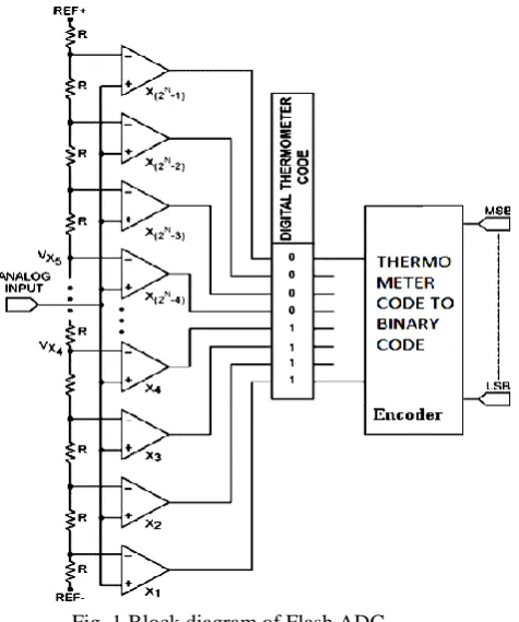
Here we improve the structure of encoder circuits to a special architecture to reduce delay and power dissipation. The block diagram of a typical flash ADC is as shown in Fig 1.
Fig. 1 Block diagram of Flash ADC
code (TC), it is called thermometer code because as the amplitude of the analog input increases the number of ones in the output increases linearly which is similar to the mercury rise in the thermometer, and the digital encoding network converts 2N – 1 inputs to N bit binary code (BC). The digital encoding network comprises 1-out-of-N code generator circuit for intermediate conversion, which is usually implemented using NAND gates or 01 generator circuits, and 2N to N bit encoder. For example, a four bit flash ADC consists of sixteen resistors generating fifteen different reference voltages for comparators. The comparators generate a fifteen bit thermometer code, which is encoded to four bits digital output using an encoder.
III.HEF (HIGH EFFICIENCY FLASH ) ADC ARCHITECTURE
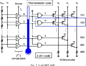
The basic idea of HEF (High Efficiency Flash ) ADC is as shown in figure below. The major blocks are comparators, thermometer code to 1 out of N code converter, 1 out of N code coverter to equivalent binary code converter.
Fig. 2 Block Diagram of HEF ADC
High Speed Low Power Comparators are used here. Thermometer Code to 1 out of N code converter is made up of NAND gates . 1 Out Of N Code to Equivalent Binary Code Converter is made of several pmos with one end connected to vdd.
Fig. 3 3- bit HEF ADC
There are 7 NAND gates 12 PMOS transistors in the encoding section of 3 bit HEF ADC. There are 4 transistors in each NAND gate .So there will be a total of 40 transistors in the encoding section.
Output from the comparators is fed into the nand section .Thermometer code will get converted into a code in which only one bit is 0 and all other bits are 1. This code is fed into a ROM encoder with PMOS corresponding to the output . When the PMOS gets a 0 at it’s gate it turns on and pulls that bit line to VDD ( 1 ). This encoder performs the encoding operations quicker than other encoders.
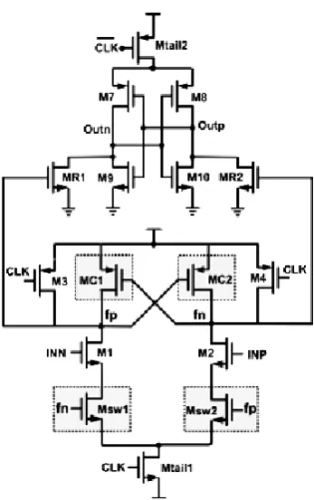
Fig. 4 High Speed Low Power Double Tail comparator
In HEF ADC High Speed Low Power Double Tail comparator is used to achieve high speed and less power dissipation.
The delay of the high speed low power doubletail dynamic comparator is significantly less when compared to conventional dynamic comparator and double tail dynamic comparator .
The power consumption of the high speed doubletail dynamic comparator is significantly less when compared to double tail dynamic comparator. But the power consumption of the high speed low power doubletail dynamic comparator is greater when compared to the power consumption of conventional dynamic comparator.
The power delay product of the high speed low power doubletail dynamic comparator is lesser than other comparator configurations.
V. RESULT AND DISCUSSION
Table 1 summarizes the delay of different ADCs, compares the power consumption of different ADCs and
Table 1 Comparison of ADC s
ADC configurations Total Power Delay Power Delay Product
Conventional Flash ADC using Conventional Dynamic
Comparator
824.326µW 2.67 µs 2.2 x 10^ - 9
Conventional Flash ADC using Double- Tail Dynamic
Comparator
20.60487mW 2.67 µs 54.190 x 10^ - 9
Conventional Flash ADC using High Speed Dynamic
Comparator
13.63mW 2.58 µs 35.165 x 10^ -9
Conventional Flash ADC using
High Speed Low Power Dynamic
Comparator
11.03mW 2.57 µs 28.347 x 10^ -9
High Efficiency Flash ADC 11.50mW 1.2 µs 13.8 x 10^ -9
The delay of the High Efficiency Flash ADC is significantly less when compared to others .
The power consumption of the High Efficiency Flash ADC is significantly less. But the power consumption of the High Efficiency Flash ADC is greater when compared to the power consumption of Conventional Flash ADC using Conventional Dynamic Comparator .
The power delay product of the High Efficiency Flash ADC is lesser than other ADC configurations
.
VI.CONCLUSION
The power dissipation and delay of an encoder plays a major role in the design of flash ADC. The encoder with an initial converter stage is designed and tested using all the input combinations from the truth table and verified. The encoder is designed and simulated using gpdk 180 nm technology using CADENCE tool. In most of the 5 bit flash ADCs in 180 nm technology, the power dissipation is more as compared to other with better speed. The encoder is designed in order to minimize the power dissipation and delay.
A comprehensive delay analysis for clocked dynamic comparators were done. Four structures of comparators namely conventional dynamic comparator, conventional double-tail dynamic comparator, high speed dynamic comparator and high speed low power dynamic comparator were analyzed .Least power delay product was obtained for high speed low power dynamic comparator. The comparators were simulated using gpdk 180 nm technology using CADENCE tool.
Flash ADCs using High speed Low power dynamic double tail comparator and with initial thermometer code conversion has highest efficiency. But it will be a great achievement if the number of transistors can be minimized .
REFERENCES
[1] M. Subba Reddy,S.Tipu Rahman ," An Effective 6 bit Flash ADC using Low Power CMOS Technology," IEEE 2013.
[2] Vinayashree Hiremath , Saiyu Ren ," A NovelUltra High Speed Recongurable Switching Encoder for Flash ADC,"in Proc. IEEE National.Aerospace and Electronics Conference (NAECON),pp 320 -323,april 2011 .
[3] D. Lee, J. Yoo, K. Choi, and J. Ghaznavi, "Fat-tree encoder design for ultrahigh speed ash analog-to-digital converters," in Proc. IEEE Midwest Symp. Circuits Syst, pp. 233236, Aug 2002.
[4] Jincheol Yoo, Kyusun Choi, Ali Tangel,"A 1-GSPS CMOS Flash A/D converter for System-on-Chip Applications", IEEE Computer society workshop on VLSI, pp 135-139,April 2001.
[6] Samad Sheikhaei, Shahriar Mirabbasi, and Andre Ivanov, "A 0.35nm CMOS Comparator Circuit For High-Speed ADC Applications",IEEE International symposium on Circuits and Systems,Vol. 6, p. 6134-6137, 2005.