ISSN (Print) : 2320 – 3765 ISSN (Online): 2278 – 8875
I
nternational
J
ournal of
A
dvanced
R
esearch in
E
lectrical,
E
lectronics and
I
nstrumentation
E
ngineering
(An ISO 3297: 2007 Certified Organization)
Vol. 5, Issue 4, April 2016
Design and Implementation of
Reconfigurable Adder Architecture, with
Reduced Area and Power Consumption
M. Pavan, Praveen J
M. Tech Student, Dept. of ECE, ALVA’S Institute of Engineering & Technology, Mijar, Moodbidri, India Associate professor, Dept. of ECE, ALVA’S Institute of Engineering & Technology, Mijar, Moodbidri, India
ABSTRACT: As the complexity of design is growing larger it is attracted by way of the reconfigurable fabrics to remedy the computational problems. The Reconfigurable computing approach provides more flexibility. As a result bettering performance of digital adder would broadly enhance the execution of binary operations. Distinct adder versions are viewed because the realistic models. In this paper, a bendy reconfigurable structure with one-of-a-kind adder versions like RCA and CSLA are implemented to type dynamically reconfigurable Hybrid adder architectures. We put in force the reconfigurable structure with the aid of exploring the regularity of the adder architectures with minimal extra multiplexers. Right here reconfigure ability has been accomplished between the adder versions.
KEYWORDS: RCA, CSLA, Adder
I.INTRODUCTION
Adders are extensively used in daily activities, computers and in many processors which are not only used in arithmetic good judgment unit but also they are used in many different components of the processor, where they are used to calculate addresses, table indices and lots of extra purposes. Adders are also used in multipliers, in excessive speed built-in circuits, in digital signal processing to execute various algorithms. Reconfigurable architecture gives the talents of each excessive performance and high flexibility. Nonetheless power consumption can also be an essential criterion which determines the affectivity of the reconfigurable architecture for use in data intensive purposes like cryptography, multimedia and signal processing. Many of the computing instruments contain signal processing procedures which consume extra power therefore it is necessary to reduce the power consumption of these devices.
Common disorders for VLSI designers are to shrink the area of the chip and expand its performance for computational functions. The impact of adders might be colossal on the total performance of the system due to the fact that they're the most copiously used accessories in digital circuits. The real time signal processing approach of the multi-media functions is carried out by the reconfigurable adders. Different adder editions are regarded as sensibleitems.
The combos of these adder architectures are employed in designing the reconfigurable architectures. This design supplies extra flexible reconfigurable adder architecture via exploring regularity of adder architectures with minimal further multiplexers. Big quantity of discipline and power consumption is greatly lowered by way of the regularity between the adder versions. This paper proposed a design of Ripple lift Adder and carry decide on Adder.
II.LITERATURESURVEY
ISSN (Print) : 2320 – 3765 ISSN (Online): 2278 – 8875
I
nternational
J
ournal of
A
dvanced
R
esearch in
E
lectrical,
E
lectronics and
I
nstrumentation
E
ngineering
(An ISO 3297: 2007 Certified Organization)
Vol. 5, Issue 4, April 2016
tractors) in the coefficient multiplier. The Common Sub-expression Elimination (CSE) algorithm reduces number of adders in the multipliers and dynamically reconfigurable filters can be efficiently implemented.
Shamsiah Suhaili et.al [09] Adders are very significant components in digital systems because of their widespread use in basic digital operations such as subtraction, multiplication and division. Hence improving performance of digital adder would extensively advance the execution of binary operations. Different adder variants are considered as the functional units. The combinations of these adder architectures are employed in designing the reconfigurable architectures. This approach provides the advantage of both better performance and high flexibility. These Flexible reconfigurable architectures includes adder variants like Ripple Carry Adder, Carry Select Adder and Carry Select Adder with common Boolean logic have been discussed here. The proposed architectures help the designer to perform efficient Design Space Exploration.
Anjaly Sukumaran et al [10] LOW-POWER, area-efficient, and high-performance VLSI systems are increasingly used in portable and mobile devices, multi standard wireless receivers, and bio medical instrumentation. An adder is the main component of an arithmetic unit. A complex digital signal processing (DSP) system involves several adders. An efficient adder design essentially improves the performance of a complex DSP system. A ripple carry adder (RCA) uses a simple design, but carry propagation delay (CPD) is the main concern in this adder. Carry look-ahead and carry select (CS) methods have been suggested to reduce the CPD of adders. Researchers in [05], [06],[07] also proposed an efficient method.
III.PROBLEMSTATEMENT
Reconfigure ability can be carried out with extraordinary levels and with combos depending on the application. In the state-of-the-art reconfigurable architectures, simplest bit width is configured. Headquartered on the variable bit width, the designer chooses targeted method constraints. Within the state-of-the-art hybrid architectures, there's no scope for dynamically settling on the architectures. Hence the present reconfigurable architectures and hybrid architectures, the designer have limited restrained scope for design area exploration as in [01], [02], [03], [04].
IV.PROPOSEDSYSTEM
Proposed structure of reconfigurable RCA-CSLA is the Figure 1. In this structure we tackle each above obstacles, implemented design not only differ the bit width however can dynamically prefer distinctive architectures there by means of lowering the area required on chip and reduces the power consumption. Within the beneath architecture uses the shared logic to reduce the chip area, right here it shares first half of CSLA logic. We are implementing this using verilog code and simulate it on Xilinx platform. And optimize the power, area, energy, and delay as in comparison with present architecture.
In RCA, Full Adders are cascaded in series such a way that the carry out from prior stage is attached to carry input of the next stage. Full Adder varieties the fundamental constructing block of RCA, and it has three inputs say ‘A’, ‘B’, ‘Cin’ and two outputs say “Sum” and “Cout”. The RCA passes from carry-in to the carry-out along the bulk gates in the critical path. The extra bendy reconfigurable adder architecture is designed by means of exploring the regularity of the adder architectures with minimal additional multiplexers. Here reconfigure ability has been done between the adder variations Ripple raise Adder and carry opt for Adder.
ISSN (Print) : 2320 – 3765 ISSN (Online): 2278 – 8875
I
nternational
J
ournal of
A
dvanced
R
esearch in
E
lectrical,
E
lectronics and
I
nstrumentation
E
ngineering
(An ISO 3297: 2007 Certified Organization)
Vol. 5, Issue 4, April 2016
Figure 1: Block Diagram of the proposed RCA-CSLA Architecture.
V.EXPERIMENTALRESULT
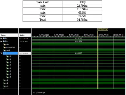
Figure 2: depicts the optimized waveform result of the proposed system. Table 1 depicts the design utilization summary for the proposed system. Table 3 depicts list for gate delay and Net Delay and the total delay of 34.78ns is obtained when compared to the existing system with delay of 35.080ns.
Table 1: Devise Utilization Summary
Devise Utilization
Number of Slices 2
Number of 4 input LUTs 4
Number of IOs 27
Number of bonded IOBs 27
Table 2 depicts the timing summary for the proposed system.
Table 2: Timing Summary
Speed Grade -4
Maximum combinational path delay 34.788ns
Timing Detail All values displayed in nanoseconds (ns)
Timing constraint Default path analysis
Delay 34.788ns (Levels of Logic = 28)
Source cin (PAD)
Destination cout (PAD)
ISSN (Print) : 2320 – 3765 ISSN (Online): 2278 – 8875
I
nternational
J
ournal of
A
dvanced
R
esearch in
E
lectrical,
E
lectronics and
I
nstrumentation
E
ngineering
(An ISO 3297: 2007 Certified Organization)
Vol. 5, Issue 4, April 2016
Table 3: Gate Delay and Net Delay
Total Gate Delay
logic 22.794ns
route 11.994ns
logic 65.5%
route 34.5%
Total 34.788ns
Figure 2: Simulation Results forthe Proposed RCA_CSA System
VI.CONCLUSION
The proposed architecture reduced the delay and area thereby reducing the overall power consumption. This design is suitable when the application is need of ultra low power in terms of leakage, low power, low area and high performance and to have a balanced design quality metrics. Furthermore carrying this kind of reconfiguarability could help in accommodating all adder variants within the same and reduced area of the regular architecture. These architectures are pervasive and can also be implemented at more than a few levels of hierarchical abstractions. The resolution of adder editions and its number of different adder editions in the sub-adder block will also be chosen or restricted as per the application requirement for bigger resolution in efficiency. Proposed architecture allows effective design space exploration compared to the existing method.
REFERENCES
[1] Ming-Hau Lee, Hartej Singh, Guangming Lu, Nader Bagherzadeh and Fadi J. Kurdahi “Design and Implementation of the MorphoSys
Reconfigurable Computing Processor”, Journal of VLSI Signal Processing Systems, Vol. 24, pp. 147–164, 2000.
[2] Jin-Fu Li and Yu-Jane Huang, “A Design Methodology for Carry-Lookahead Adders with Reconfigurability”, IOSR journal on VLSI, 2000.
[3] Stefania Perri, Giuseppe Cocorullo, “A High-Speed Energy-Efficient 64-Bit Reconfigurable Binary Adder”, Ieee Transactions on Very Large
ISSN (Print) : 2320 – 3765 ISSN (Online): 2278 – 8875
I
nternational
J
ournal of
A
dvanced
R
esearch in
E
lectrical,
E
lectronics and
I
nstrumentation
E
ngineering
(An ISO 3297: 2007 Certified Organization)
Vol. 5, Issue 4, April 2016
[6] Agarwal, M. Agrawal, N. Alam, M.A., "A new design of low power high speed hybrid CMOS full adder," Signal Processing and Integrated
Networks (SPIN),International Conference, pp. 20-21, 2014.
[7] S.Karthick, S. Valarmathy, E. Prabhu, “Reconfigurable Adder Architectures for Low Power Applications”,International Journal of Computer
Applications, Vol. 4, 2014.
[8] N.Durairajaa, J.Joyprincy, M.Palanisam, “Design of Low Power and Area Efficient Architecture for Reconfigurable FIR Filter”, International
Journal of Recent Technology and Engineering (IJRTE), Vol. 2, Issue-1, 2013.
[9] Pallavi Malipatil,“Reconfigurable Low Power RCA-CSLA Adder Architecture”, International Journal for Technological Research in
Engineering Vol. 2, Issue 9, 2015.
[10] Anjaly Sukumaran, “Area Delay Power Efficient Carry Select Adder On