1
Role of structure and composition on the performances of p-type tin
2
oxide thin-film transistors processed at low-temperatures
3
R. Barros1,2, K. J. Saji1,3, J. C. Waerenborgh4, P. Barquinha1, L. Pereira1, R. Martins*1
4
and E. Fortunato1*
5
* Correspondence: Prof. Elvira Fortunato ([email protected]; Professor Rodrigo Martins ([email protected])
6
1CENIMAT/I3N, Departamento de Ciência dos Materiais, Faculdade de Ciências e Tecnologia, FCT,
7
Universidade Nova de Lisboa and CEMOP-UNINOVA
8
Campus da Caparica, 2829-516 Caparica (Portugal)
9
*E-mail: [email protected];
10
2Hovione, Campus do Lumiar, Edifício S, Estrada do Paço do Lumiar, 1649-038 Lisboa, Portugal
11
3 Cochin Univ Sci & Technol, Int Sch Photon, Kochi 682022, Kerala, India
12
4Instituto Tecnológico e Nuclear / CFMC, Estrada Nacional 10, 2686-953 Sacavém, Portugal
13
14
15
Abstract: This work reports the role of structure and composition on the determination of the
16
performances of p-type SnOx TFTs deposited by rf magnetron sputtering at room temperature,
17
followed by a post-annealed step up to 200ºC at different oxygen partial pressures (Opp), between
18
0% and 20%, but where the p-type conduction was only observed between 2.8-3.8%. The role of
19
structure and composition were evaluated by XRD and Mössbauer spectroscopic studies. The study
20
allows to identify the best phases/compositions and thicknesses (around 12 nm) to be used that lead
21
to the production of TFTs with a bottom gate configuration, on glasses coated with conductive
22
Indium Tin Oxide, followed by Aluminium Titanium Oxide dielectric layer with saturation mobility
23
of 4.6 cm2V-1s-1 and on-off ratio above 7×10⁴, operating at the enhancement mode with a saturation
24
voltage of -10 V.
25
Keywords: p-type TFT, p-type oxide semiconductors, SnO electrical properties; Oxide structure
26
analysis
27
28
1. Introduction
29
Oxide electronics or in more generic terms transparent electronics, is emerging as an appropriate
30
alternative to amorphous silicon (a-Si:H) and organic semiconductors, especially for thin film
31
transistors (TFTs) and more complex electronic circuits. Oxide semiconductors are a promising class
32
of TFT materials that have made impressive demonstration in display applications in a relatively
33
short time, challenging silicon in the flexible electronics field. Although some initial attempts during
34
the 60s were done for SnO2,[1] and ZnO,[2]TFT channel layers, only forty five years later, with the
35
work of Hosono,[3] Wager,[4] Carcia,[5] and Fortunato,[6] a significant worldwide interest appeared,
36
especially for active matrix for organic light emitting diodes (AMOLED) technology, both in industry
37
and academia. Oxide semiconductors have unique electronic properties like high mobility
38
irrespective to the structure nature and excellent uniformity and homogeneity in device parameters
39
associated to a low or room temperature deposition process allowing the use of low cost and flexible
40
substrates such as polymer or even paper.[7]
41
However, there is no report on p-type oxide TFTs with performance similar to n- type, which is
42
mainly limited by the low hole mobilities.[8] Achieving high performance p-type oxide TFTs will
43
definitely promote a new era for electronics in rigid and flexible substrates, away from silicon.
44
Moreover, it will shape the electronics of tomorrow by allowing the production of complementary
45
metal oxide semiconductors (CMOS), a key device to fuel the microelectronics revolution in the
so-46
called technologies of information and communication, by allowing the use of highly compact circuits
47
with low power consumption.
48
At present, almost all reported oxide TFTs are based on n-channel devices.[1-9] The carrier
49
conduction path (valence band) in p- type oxides is mainly formed from the oxygen p asymmetric
50
orbitals, which severely limit the carrier mobility and lead to poor TFT performance. Cu2O is a p-type
51
oxide with mobility exceeding 100 cm2V-1s-1.[10,11] However, TFTs prepared from Cu2O have
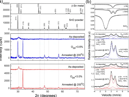
field-52
effect mobilities and on-off current ratio below 1 cm2V−1s−1 and 102 respectively, due to difficulty in
53
controlling the hole density in channel layer.[11-13] While conventional passive applications
54
require the maximum possible hole density for optimal conductivity, the channel layer requires a low
55
hole density in order to modulate the channel conductance by an applied electric field. Most of
56
organic TFTs reported in the literature are p-type.[14,15] Even though organic TFTs have been the
57
topic of intense research for the past few decades, the overall performance is still poor compared to
58
oxide TFTs, namely low mobilities (< 2 cm2V-1s-1),[16] poor stability and device-to-device variability.
59
Additionally, the high operating voltage is a disadvantage for portable, battery-powered device
60
applications.[15,16] Moreover, the n-type organic semiconductors have even much lower mobilities
61
(10-3 to 10-2 cm2V-1s-1), limiting their use in applications such as CMOS.[17]
62
In this paper, we report the fabrication of high-performance oxide TFTs using p-type SnOx
63
channel layer deposited by rf magnetron sputtering at room temperature that is post-annealed up to
64
200ºC. SnO has a specific electronic structure associated with the presence of divalent tin (SnII), in a
65
layered crystal structure.[18,19] SnO has an indirect band structure with major contribution from Sn
66
5s and O 2p orbitals near the valence band maximum (VBM) and Sn 5p orbitals towards the
67
conduction band minimum (CBM). The origin of p-type conductivity in SnO is mainly attributed to
68
the Sn vacancy and the O interstitial where tin is in Sn2+ oxidation state.[18,19] If there is excess
69
oxygen in the film, some cations will be transformed into Sn3+ to maintain electrical neutrality. This
70
process is considered as Sn2+ capturing a hole and forming weak bonded holes which are located
71
inside the bandgap near the top of the valence band as localized acceptor states.[20,21]
72
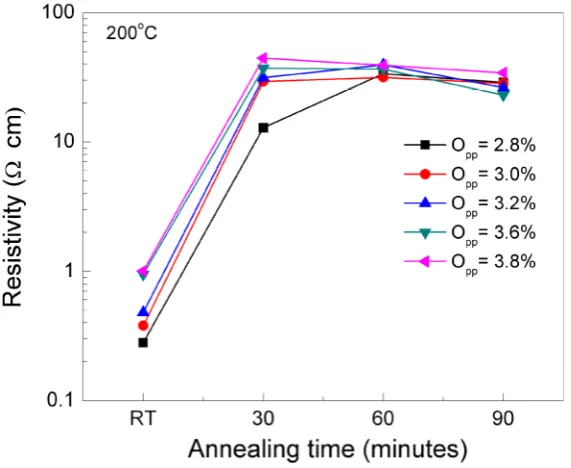
73
For a set of practical applications, there are a clear demand for p-type TFT able to match the
74
requirements to grow ultra-low power electronics systems, whose key components are based CMOS
75
technology [22]. Apart from that, the emerging flexible electronics, is pushing for processing devices
76
at low process temperatures, together with high mobility and high on-off ratios [7].
77
TFTs based on p-type SnOx are expected to fulfill these requirements due to the particular nature
78
of band structure. [20,21] Contributions from Sn 5s states to VBM could offer appreciable hole
79
mobility in this material, without using high processes temperature [23,24]. In the present work, SnOx
80
based TFTs are prepared by an industrial friendly rf magnetron sputtering system at room
81
temperature (RT), without any intentional substrate heating during the growth process, aiming to
82
understand the role of structure, surface finishing and composition in producing high stable TFT with
83
high electronic performances, such as field effect mobility and on-off- current ratios.
84
2. Materials and Methods
85
Prior to process the TFT devices, the material in which the channel is based was processed and fully
86
analyzed, concerning their structure, morphology, composition and electro-optical properties,
87
aiming to determine the best conditions to grow the channel layers of the TFT with a bottom gate
88
configuration
89
Films Preparation
90
SnOx films were deposited on glass substrates using a computer controlled rf magnetron
91
sputtering system using a metallic tin target (99.999% pure). Depositions were carried out in a
92
controlled atmosphere of oxygen and argon. Sputtering power to metallic tin target was fixed at 40
93
W and substrates were rotated at a speed of 40 rpm. Experiments were performed by varying Opp
94
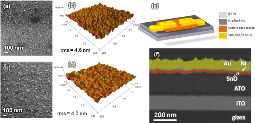
deposition chamber, keeping the total deposition pressure constant at 0.2 Pa. At this condition, the
96
deposition rate was 40 Å/min.
97
Structure and composition studies
98
X-ray diffraction analysis was performed on tin oxide thin films deposited on glass substrates,
99
using PANalytical X’Pert Pro system, as depicted in Fig.1.
100
101
Figure 1: (a) XRD patterns of deposited SnOx thin films. (b) Transmission 119Sn Mössbauer spectra of bulk
102
samples and CEMS spectra of as-deposited and annealed SnOx films deposited at 3.0% and 3.6% Opp.
103
104
119Sn Mössbauer spectra analysis
105
The films were analyzed by 119Sn conversion-electron Mössbauer spectroscopy (CEMS) at room
106
temperature placing them inside a proportional backscatter detector RIKON-5 (Wissel) in flowing
107
5%CH4-95% He gas mixture (see figure 1b). Both CEMS and transmission Mössbauer spectra were
108
collected using a conventional constant acceleration spectrometer and a 5 mCi Ca119mSnO3 source. The
109
velocity scale was calibrated using a 57Co (Rh) source and an α-Fe foil. The Sn isomer shifts (IS) are
110
given relative to BaSnO3 reference material at 295 K and obtained by adding 0.031 mm/s to the IS
111
relative to the source. The spectra were fitted to Lorentzian lines using a non-linear least-squares
112
method. The set of estimated parameters extracted are depicted in table 1.
113
114
Table 1. Estimated parameters from the transmission 119Sn Mössbauer spectra of bulk samples and
115
CEMS spectra of films taken at 295K.
116
Sample IS [mm/s]
QS [mm/s]
Γ
[mm/s] Sn phase
I [%]
SnO2 bulk 0.01 0.56 1.34 - 100
α-SnO bulk 2.67
-0.03 1.34 0.58 0.98 0.77 αSnO-SnO 2
-Sn metal 2.56 - 1.03 - 100
Film
Opp=3.0%, RT
2.76 0.11 2.56 1.87 0.52 - 1.04 0.84 1.3 SnO SnO2 -Sn 65 15 20 Film
Opp=3.0%,
200oC, 30 min
2.7 0.08 2.56 1.38 0.59 - 0.79 0.7 1.35 SnO SnO2 -Sn 81 8 11 Film
Opp=3.6%, RT
2.73 0.11 2.56 1.82 0.53 - 1.02 0.81 1.3 SnO SnO2 -Sn 78 15 7 Film
Opp=3.6%,
200oC, 30 min
2.7 0.06 1.34 0.48 0.82 0.85 SnO SnO2 88 12
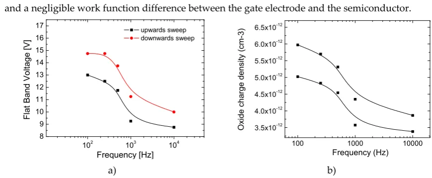
IS (mm/s) isomer shift relative to metallic BaSnO3 at 295 K; QS (mm/s) quadrupole splitting; Γ (mm/s)
117
line-width; I relative area. Estimated errors ≤ 0.02 mm/s for IS, QS, Γ and <2% for I.
118
Electrical studies
119
It is essential to study the electrical properties of the material in order to understand the charge carrier
120
type and transport properties. Hall Effect measurement is the most commonly used technique to
121
identify the charge carrier and carrier mobility in the material. In contrast to n-type oxides, Hall
122
measurement does not give reliable results for p-type oxides, primarily because of very small drift
123
mobility of holes. Moreover, when both electrons and holes are present in a semiconductor sample,
124
both charge carriers experience a Lorentz force in the same direction. So, both electrons and holes
125
will pile up at the same side of the sample and consequently the measured Hall voltage depends on
126
the relative mobilities and concentrations of holes and electrons. Hall mobility for an ambipolar
127
semiconductor is thus given by,
128
n2 2p Hall n p
n
p
n
p
μ
μ
μ
μ
μ
⋅
− ⋅
=
⋅
+ ⋅
(1)
129
130
where n, p, µn and µp represent electron density, hole density, electron drift mobility and hole drift
131
mobility respectively. This suggests a considerable reduction in Hall mobility in an ambipolar
132
semiconductor compared to the actual drift mobilities of the charge carriers.
133
In the present analysis, RT deposited samples have shown fluctuations in the sign and magnitude of
134
Hall coefficient. Typical carrier mobilities were of the order of 10-1 cm2 V-1 s-1. Because of the ambipolar
135
nature of the RT deposited films [25], these results suggest that Hall measurement of SnOx films
136
highly underestimates the actual carrier mobility. After annealing up to 200oC for 30 minutes, films
137
prepared in the Opp of 2.8-3.8% have shown positive Hall coefficient consistently. There was no
138
change in Hall coefficient sign even though the magnitudes were shown small fluctuations. This
139
suggests a considerably large density of holes compared to the density of electrons. Figure 2 shows
140
the resistivity variation of as prepared and annealed SnOx films.
141
143
Figure 2: Variation in the resistivity of SnOx films as a function of annealing time.
144
145
As observed in the Mossbauer spectra of RT deposited films, RT samples consist of metallic tin, SnO
146
and SnO2 phases. In this condition, both electrons and holes can contribute to the charge transport in
147
the system. At 200 °C annealing in air, oxygen atoms incorporate to the films which oxidizes with
148
metallic tin leading to SnO phase formation with reduction in electron density and increase in hole
149
density. This may be the reason for initial increase in the resistivity of the films. In this case, the
150
material has large density of holes compared to the density of electrons which results in positive Hall
151
voltage with typical Hall mobility of 2 cm2 V-1 s-1.
152
Annealing at still higher temperatures cause again a decreasing tendency in material resistivity (not
153
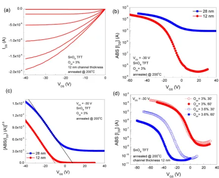
shown here). This time, it is because of the phase transformation of the material from SnO (p-type) to
154
SnO2 (n-type). Actual carrier mobility must be much higher than the measured hall mobility value.
155
156
157
Optical studies
158
Optical transmittances of RT deposited films were very poor in the visible region, mainly because of
159
the presence of large concentration of metallic tin in the films (Figure 4a). Annealing up to 200oC for
160
30 minutes considerably increased the optical transmittance in the visible region. However, still the
161
maximum transmission was around 50%. SnO has been reported as an indirect bandgap material
162
with a direct bandgap value of around 2.5 eV and indirect band gap value around 1 eV. Whereas,
163
SnO2 is a direct bandgap material with bandgap value around 3.6 eV.
164
The optical absorption coefficient (α) of semiconductors generally follows a relationship of the form,
165
α
⋅ ⋅ =
h
ν
const h
⋅ ⋅ −
(
ν
E
g)
r (2)166
where hν denotes the photon energy, Eg the optical band gap, and r a constant depending on the type
167
of optical transition in the material. The Eg value is then obtained by linearly extrapolating the plot of
168
1/
(
α
⋅ ⋅
h
ν
)
rwere analyzed with r = ½ (direct transition) and r = 2 (Indirect transition). Estimated direct bandgap
170
values are in the range of 2.6 - 2.75 eV for annealed films (figure 3b and 3c). However, the presence
171
of a narrow gap indirect band results considerable optical absorption below these estimated values.
172
The indirect values estimated from a plot of vs results 1.6 - 2.2 eV which is around 1 - 0.55 eV
173
below the corresponding direct bandgap values (figure 3d). These values are close to the reported
174
bandgap values for SnO films. Small variations in these values could be understood on the basis of
175
fractional variations of various phases (metallic tin, SnO and SnO2) in the films.
176
177
178
179
Figure 3: (a) Optical transmission of as prepared and annealed SnOx films. (b) Plot of vs for direct bandgap
180
estimation. (c) Estimated direct bandgap values and (d) indirect bandgap values.
181
182
Devices architecture and structure
183
Surface morphology of TFT channel layers was analyzed by ZEISS Auriga SEM-FIB and Asylum
184
MFP-3D AFM, as depicted in fig.4.
185
Bottom gate TFTs were fabricated on glass substrates coated with 150 nm thick layer of sputtered
186
ITO and a 220 nm thick layer of aluminium-titanium oxide (ATO). SnOx channel layer
187
(width/length=50 m/50 m) was deposited over this by rf magnetron sputtering. Ni/Au (9 nm/60
188
nm) stacks deposited by electron beam evaporation were used as source and drain electrodes. After
189
deposition, devices were annealed in air up to 200oC for 30 minutes inside a tubular furnace (see
190
192
Figure 4. SEM images of post-annealed TFT channel layers prepared at Opp of (a) 3.0% and (b) 3.6%.
193
Corresponding AFM images of the TFT channel layers are shown in (c) and (d). (e) Schematic illustration of SnOx
194
TFT structure employed for the present study. (f) Cross-sectional SEM image of the SnOx channel TFT.
195
196
TFT electrical characterization was performed with an Agilent 4155C semiconductor parameter
197
analyzer and a Cascade Microtech M150 microprobe station inside a dark box at ambient atmosphere.
198
199
Capacitance measurements
200
CV measurements have been done in TFT by short circuiting the drain and source terminals. By doing
201
so we enhance the overall capacitance measured allowing a better discrimination on the data
202
achieved. Under these conditions, we assume an electrical model consisting in a contact resistance RC
203
(equal for drain and source regions, since we have a symmetric device) in series with the combination
204
of two parallel RC resonators as depicted in the sketch of figure 5a. One represents the semiconductor
205
channel capacitance (CS) that varies dynamically, depending on the extension of the
206
accumulation/depletion layer. The other is the interface trap capacitance (Cit) in series with the
207
corresponding associated interface resistance Rit, both depending on the interface defects given by:
208
2 2 2 0
1 ) ( )
(
it it it
D q Q
V
dx dV
V C
τ
ω
ρ
εε
ρ
+ = =
= (2)
209
Where Dit is the interface trap density, τit=Rit×Cit is the trap response time. Finally, we have in series
210
the insulator geometric capacitance (Cox). As the frequency tends to steady state condition, we have
211
almost Cit in parallel with Cs and the resulting capacitance in series with Cox. Therefore, for not perfect
212
semiconductors (basically, the amorphous ones) by using a frequency modulation less than the
213
relaxation frequency of the semiconductor (
0
2
1
2
1
ε
ε
πρ
π
B s B Sr
C
R
f
=
=
, where RB is the channel bulk214
resistance), we expect that capacitance data achieved to be influenced by the number and nature of
215
the interface defects, turning visible more and more defect states as the frequency decreases. The only
216
condition the charge penetration depth. That is, the values of the capacitance can be channel thickness
218
conditioned for devices whose thickness is in the range of few nanometers. On the other hand, at very
219
high frequencies, Cs dominates and Cit≅ 0, being now relevant the role of Ritin parallel with Cox. In
220
this case the capacitance-voltage curves can be distorced due to charging effects, leading to a decrease
221
or even to a not well-defined flat capacitance maximum (Cmax), as observed in the normalized CV
222
plots of figure S3b for different frequencies and on the behaviour of Cmax with the frequency, depicted
223
in figure S3c. In the same picture it is also plotted the transfer characteristics of the p-type TFT under
224
analysis (picture above whose vertical scale is on the right side of the figure). Besides the hysteresis
225
that we associate to the role of interface defects, we notice that at a frequency of about 100 Hz the
226
capacitance tends to reach a flat behaviour and the hysteresis voltage shift is enhanced, following a
227
similar trend as the one of the transfer I-V TFT characteristics. We associate this behaviour to interface
228
localized states that only respond at frequencies below fr as expected.
229
230
a)
231
b) c)
Figure5. a) Sketch of the cross section of the p-type TFT showing half of the equivalent electrical circuit based
232
on RC resonators b) Normalized CV plot for several frequencies (below), showing also the IV transfer
233
characteristic of the TFT (above); c) The Maximum capacitance (Cmax) achieved as a function of the frequency
234
used.
235
236
Apart from that we notice that the minimum capacitance is not fully flat. This behaviour we associate
237
to the small thickness of the semiconductor (≤ 12 nm) that limits the maximum dimension of the
238
depletion region we can get. As the possible maximum width of depletion region is 12 nm (the
239
semiconductor thickness), this means that the minimum capacitance of the system won’t be much
240
lower than the total capacitance.
241
242
From the CV plots depicted in Fig. 5 we could also estimate the flat band voltage shift and the oxide
243
charge density (proportional to defect density) as a function of the frequencies used, as depicted in
244
-30 -20 -10 0 10 20
0.90 0.95 1.00 1.05
Id
(A
)
100 Hz 250 Hz 500 Hz 1 kHz 10 kHz 100 k Hz
C
/C
m
ax
[N
o
rm
al
iz
ed
C
apa
ci
ta
n
ce
]
Voltage Vgs (V)
VD S=-30 V
IDS
10-9 10-8
10-7 10-6 10-5 10-4
102 103 104 105
420 430 440 450 460 470 480
C
apa
ci
ta
nce
(
pF
)
Fig. 6. There we indicate the two values determined for each frequency due to the hysteresis, defining
245
so the window range of variation of such parameters. For this calculation we assumed a Na=1017cm-3
246
and a negligible work function difference between the gate electrode and the semiconductor.
247
a) b)
Figure6. a) Flat band Voltage dependence on the frequency; b) Oxide charge density as a function
248
of the frequency.
249
250
Both plots show a similar dependence on frequency as expected, leading to an enhancement on the
251
flat band voltage and on the oxide charge density as the frequency decreases.
252
253
3. Results and Discussion
254
The SnOx films were prepared at different oxygen partial pressures (Opp) between 0% and 20%,
255
but the p-type conduction was observed only between 2.8-3.8%. The films deposited with Opp below
256
2.8% were metallic with poor adhesion to the substrate. Those deposited above 3.8% were highly
257
resistive, showing n-type conduction after annealing above 200 °C. This is well understood based on
258
tin oxide’s two well-known forms: SnO (p-type conduction) and SnO2 (n-type conduction). Since a
259
metallic tin target was used for sputtering, very low Opp was not sufficient to fully oxidize the film. It
260
is believed that Opp in the range of 2.8-3.8% are suitable to form SnO phase and for Opp 3.8% favours
261
SnO2 formation. Since TFTs were prepared for two Opp, namely at 3.0% and 3.6%, most of the
262
materials characterizations were performed using the films deposited at these conditions.
263
Figure 1 (a) shows the x-ray diffraction (XRD) pattern of the films (120 nm thickness) using Cu
264
Kα line. It shows that RT films have large portion of metallic tin with very small SnO phase. After
265
annealing up to 200°C for 30 minutes in air, part of metallic tin seems to be oxidized to SnO phase.
266
The XRD patterns obtained (in the similar conditions) from SnO powder and metallic Sn are also
267
shown in figure 1.
268
In order to evaluate the structure, composition of the films and the ratio of SnO and SnO2 phases
269
present in the TFT channel layer, 119Sn Mössbauer spectroscopic studies were performed for the first
270
time in this type of work, whose results are shown in figure 1 (b). Transmission Mössbauer spectra
271
of bulk metallic Sn, SnO and SnO2 samples (figure 1b, table 1) were obtained in order to compare the
272
corresponding hyperfine parameters with those of the phases detected in the films by
conversion-273
electron 119Sn Mössbauer spectroscopy (CEMS). The spectra of the bulk samples are identical to
274
those reported in the literature for β-Sn, α-SnO and SnO2, respectively.[26,27] The α-SnO spectrum
275
shows a small contamination of SnO2 at lower Doppler velocities, which is a common contamination
276
of α-SnO when exposed to air and is easily detectable by Mössbauer spectroscopy due to the higher
277
recoilless fraction of Sn4+ in SnO2 as compared to Sn2+ in α-SnO.[28,29] The typical asymmetry of the
278
α-SnO doublet, the high velocity peak having a higher relative area than the low-velocity peak, is
279
also observed.[27-30]
280
281
102
103
104 8
9 10 11 12 13 14 15 16 17
F
la
t Ban
d Voltage
[V]
Frequency [Hz] upwards sweep downwards sweep
100 1000 10000
3.5x10⁻¹²
4.0x10⁻¹²
4.5x10⁻¹²
5.0x10⁻¹²
5.5x10⁻¹²
6.0x10⁻¹²
6.5x10⁻¹²
Oxide cha
rge d
ensity (cm
-3)
The CEMS spectra of the samples could be fitted by three contributions with typical isomer shifts
282
(IS) of Sn4+, Sn2+ and metallic Sn. For all spectra, the estimated IS of the absorption peak due to metallic
283
Sn (table S1) is very similar to that of β-Sn, confirming the presence of this phase in the films as
284
corroborated by XRD. The observed IS, quadrupole splitting (QS) and the line widths of Sn2+ in the
285
as-deposited samples are higher than the corresponding parameters for bulk α-SnO. After annealing,
286
the decrease of IS and QS lead to values, which within experimental error, are close to those of
287
crystalline α-SnO. This suggests that the Sn2+ oxide present in the as-deposited film is amorphous and
288
after annealing up to 200ºC crystalline α-SnO is formed. This is in agreement with XRD data which
289
shows this phase in the annealed samples while in the as-deposited films only β-Sn is detected. The
290
estimated QS and line widths in the amorphous SnO are higher than in crystalline α-SnO denoting a
291
more asymmetric environment and a higher diversity of near neighbour configurations of Sn2+ in the
292
amorphous lattice. Furthermore, no asymmetry is observed for the Sn2+ oxide doublet in the as
293
deposited sample as expected for an amorphous phase. As crystalline α-SnO is formed, asymmetry
294
of the corresponding doublet becomes evident.
295
296
Mössbauer data, in agreement with XRD data, show that in the as-deposited films most Sn is
297
present as amorphous SnO and metallic β-Sn. Minor amounts of SnO2, only detected by CEMS, are
298
also present. The IS and QS of this SnO2 deduced from the spectra are slightly different from those of
299
bulk SnO2 probably due to poor crystallinity of this oxide in the film. Even though the recoilless
300
factors of β-Sn, SnO and SnO2 in films are not exactly known, these factors are not expected to be very
301
different for the same species in the different samples. So, the fraction of Sn atoms in each phase
302
should follow the same variation, with annealing or with Opp during deposition, as the relative areas
303
of the corresponding contributions to the spectra. Not surprisingly, the fraction of Sn present as β-Sn
304
is lower in the film deposited at higher Opp (3.6%), than in those deposited at 3.0%. Annealing up to
305
200ºC not only crystallizes amorphous SnO to form α-SnO but also oxidizes β-Sn to α-SnO. So, it
306
suggests that the TFT channel layer is mainly composed of SnO phase with a smaller contribution
307
from metallic tin and hence we can represent the channel material composition as SnOx with 1<x<2.
308
309
In order to understand the surface morphology of the channel layer, we performed scanning
310
electron microscopy (SEM) and atomic force microscopy (AFM) of the real channel layer in the TFTs
311
after annealing. The surface microstructures obtained from the films deposited at 3.0% and 3.6% Opp
312
are shown in figure 2. Even though there is no difference in the shape of the grains as evidenced by
313
both techniques, the size of the grains obtained from the films deposited at Opp=3.0% is slightly lower
314
than those deposited at Opp=3.6%. The route mean square roughness (4.6 nm) of the films deposited
315
at Opp=3.0% is slightly higher than that deposited at 3.6% (4.3 nm). Cross-sectional SEM image
316
obtained from the TFT prepared at 3.0% Opp (figure 2f) shows perfect coverage of SnOx channel layer
317
over the insulator surface with highly compact, uniform and homogeneous thin film without visible
318
defects.
319
320
Bottom gate TFTs were fabricated using aforementioned SnOx films as channel layers (~28 nm
321
thickness) deposited at 3.0% and 3.6% Opp, which were annealed in air up to 200°C for 30 minutes
322
inside a tubular furnace. Despite the high saturation mobility (4.3 cm2V-1s-1) the on-off ratio was very
323
poor (3×101) and TFTs operated in depletion mode, which may be due to a large hole density in the
324
channel layer, limiting the channel modulation.
325
326
TFT performance was improved by reducing the channel thickness to ~12 nm. The output
327
characteristics (IDS-VDS) of such TFT (Opp=3.0%) given in figure 7a shows excellent p-channel
328
behaviour. The gate voltage was varied from 0 V to -50 V in -10 V steps. Very small IDS at zero gate
329
voltage indicates an almost closed channel. On increasing the gate voltage to higher negative values,
330
holes accumulated at the channel-insulator interface forms a conduction path between source and
331
drain. These TFT exhibits hard saturation at large VDS, which is similar to pinch off in usual
field-332
334
335
Figure 7. (a) Output characteristics of SnOx p-channel TFT. The gate voltage is varied from 0 V to -50
336
V in -10 V steps. (b) Transfer characteristics of SnOx p-channel TFT with different channel thickness.
337
(c) Plot of square root of drain current, at VDS= -30 V, for evaluating saturation mobility and threshold
338
voltage. (d) Transfer characteristics of SnOx p-channel TFT (channel thickness 12 nm) for different
339
annealing time
.
340
341
TFT parameters (see table 2) were extracted from the transfer characteristics (ABS(IDS)-VGS) of
342
the p-channel TFTs for the different Opp and annealing times used, for devices annealed at 200°C
343
(figures 7 b and 7c). The field effect mobility (μFE), extracted from the slope of the linear region of the
344
IDS-VGS plot, was 3.3 cm2V-1s-1 for the TFT with 12 nm channel thickness. The saturation mobility (),
345
extracted from [ABS (IDS)]0.5 - VGS plot at VDS= -30 V, was 4.6 cm2V-1s-1 (figure 7c). With the
346
improvement in mobility values, threshold voltage shifted from 8.1 V (28 nm thick channel) to -10 V
347
on reducing the channel thickness to 12 nm. Negative threshold voltage indicates the enhancement
348
mode operation of the p-channel TFTs. Moreover, the off current of the p-type TFTs decreased by
349
several orders by reducing channel thickness which results in good switching action by increasing
350
on-off ratio from ~102 to 7×10⁴. Figure 7d shows the transfer characteristics of the devices processed
351
at different Opp and for different annealing times. The data depicted show thatthe best device
352
performances are achieved when using Opp of about 3%, and annealing times of around 30 minutes
353
are more than enough to process devices with excellent stable mobilities and large on-of current
354
rations.
355
Table 2. Electrical properties of SnOx p-channel TFTs for different annealing time (channel
357
thickness 12 nm)
358
Annealing Conditions
Oxygen Partial Pressure [%]
Field Effect Mobility [cm2 V-1 s-1]
Saturation Mobility [cm2 V-1 s-1]
Threshold Voltage [V]
On-Off ratio
200 oC, 30 min 3.0 3.3 4.6 -10 7×10⁴
200 oC, 60 min 3.0 2.2 2.6 -7.2 9×10⁴
200 oC, 30 min 3.6 0.16 0.28 -29 2×10⁵
200 oC, 60 min 3.6 0.02 0.03 -38.6 3×10⁴
359
The p- channel oxide TFTs fabricated at relatively low temperature in the present work show
360
excellent performance, which can be made even on plastic and paper substrates, surpassing the ones
361
known processed also at low process temperatures, compatible with low cost flexible substrates, such
362
as paper. Moreover, the very high on current of these devices makes them ideal for AMOLED driving
363
circuits where a TFT must supply sufficient hole current to the anode of the OLED. In addition, these
364
SnOx TFTs show excellent electrical stability even without any passivation layer.
365
Figure 8 shows the transfer curves of TFTs measured at different days after their fabrication. It
366
is clear from the figure that, these TFTs are very stable in operation without significant variations in
367
threshold voltage and mobility.
368
369
370
371
Figure 8. Transfer characteristics of SnOx p-channel TFT measured at different days after device
372
fabrication (a) and corresponding variations in saturation mobility and threshold voltage (b).
373
4. Conclusions
374
In summary, we have fabricated high performance p-channel oxide TFTs (highly reproducible)
375
on glass substrates using SnOx channel layer, for which the proper process conditions that lead to the
376
best material phase composition were selected. The SnO phase was identified and quantified by the
377
first time by two independent techniques, XRD and Mossbauer spectroscopy, corroborating the
p-378
type oxide semiconductor behaviour obtained in the TFTs. The TFTs fabricated in this work have
379
shown typical saturation mobility of 4.6 cm2V-1s-1 and on-off ratio above 7×10⁴, which are the highest
380
of fully transparent CMOS associated with all the main advantages offered by transparent/oxide
382
electronics.
383
384
Author Contributions: conceptualization, E. Fortunato and K. J. Saji; methodology, R. Martins, K. J. Saji;, R.
385
Barros; Structure, morphology, electrical and optical characterization, R. Barros, P. Barquinha; Mössbauer
386
spectra analysis J. C. Waerenborgh; validation, E. Fortunato, P. Barquinha, R. Barros, K. J. Saji; formal analysis,
387
R. Barros, P. Barquinha; investigation, R. Barros, P. Barquinha, L. Pereira; K. J. Saji; resources, E. Fortunato, R.
388
Martins; data curation, P. Barquinha, R. Barros; writing—original draft preparation, J. Saji; R. Martins; writing—
389
review and editing, R. Martins; visualization, E. Fortunato, R. Martins, K. J. Saji; supervision, E. Fortunato;
390
project administration, E. Fortunato; funding acquisition, E. Fortunato”,.
391
Funding: This work was partially supported by the European Commission under project INVISIBLE (Advanced
392
Grant from ERC nº 228144); BET-EU (H2020-TWINN-2015, GA 692373); TREND (ERC-StG-2016, grant GA
393
716510); 1D Neon (H2020-NMP-2015-IA, grant 685758-21D). We also acknowledge the FEDER funds through
394
the COMPETE 2020 Programme under the project UID/CTM/50025/2013). The authors K. J. Saji thanks
395
Portuguese Ministry of Science and Technology (FCT-MCTES) for offering research grants through the
396
fellowships SFRH/BPD/62942/2009.
397
Acknowledgments: The authors would like to thanks J. Pinto for the support giving in measuring the XRD of
398
the films processed as well as the support given by the CENIMAT technical and administrative staff along the
399
present study.
400
Conflicts of Interest: The authors declare no conflict of interest. The funders had no role in the design of the
401
study; in the collection, analyses, or interpretation of data; in the writing of the manuscript, or in the decision to
402
publish the results.
403
References
404
1. Klasens, H. A.; Koelmans, H. A Tin oxide Field-Effect Transistor. Solid-State Electron. 1964, 7, 701-2.
405
2. Boesen, G. F.; Jacobs, J. E. ZnO Field Effect Transistor. Proc. IEEE 1968, 56, 2094-
406
3. Nomura, K.; Ohta, H.; Takagi, A.; Kamiya, T.; Hirano, M.; Hosono, H. Room-temperature fabrication of
407
transparent flexible thin-film transistors using amorphous oxide semiconductors. Nature 2004, 435, 488.
408
4. Hoffman, R. L.; Norris, B. J.; Wager, J. F. ZnO-based transparent thin-film transistors. Appl. Phys. Lett.
409
2003,82, 733.
410
5. Carcia, P. F.; McLean, R. S.; Reilly, M. H.; Nunes, G. Transparent ZnO thin-film transistor fabricated by rf
411
magnetron sputtering Appl. Phys. Lett. 2003,82, 1117.
412
6. Fortunato, E.; Barquinha, P. ; Pimental, A.; Goncalves, A. ; Marques, A.; Pereira, L.; Martins, R. Fully
413
transparent ZnO thin-film transistor produced at room temperature Adv. Mater. 2005, 17, 590.
414
7. Martins, R.; Ferreira, I.; Fortunato, E. Electronics with and on paper, Phys. Status Solidi-RRL, 2011,5, 332-.
415
8. Ogo, Y.; Hiramatsu, H.; Nomura, K. ; Yanagi, H.; Kamiya, T. ; Hirano, M.; Hosono, H. p-channel
thin-416
film transistor using p-type oxide semiconductor, SnO. Appl. Phys. Lett. 2008, 93, 032113
417
9. Fortunato, E.; Martins, R. Where science fiction meets reality? With oxide semiconductors! Phys. Status
418
Solidi-RRL, 2011,5, 336.
419
10. Fortin, E.; Weichman, F. L. Hall effect and electrical conductivity of Cu2O monocrystals. Can. J. Phys.
420
1966, 44, 1551.
421
11. Matsuzaki, K.; Nomura, K. ; Yanagi, H.; Kamiya, T. ; Hirano, M. ; Hosono, H. Epitaxial growth of high
422
mobility Cu(2)O thin films and application to p-channel thin film transistor. Appl. Phys. Lett. 2008, 93,
423
202107.
424
12. Deuermeier, J.; Fortunato, E.; Martins, R.; Klein, A. Energy band alignment at the nanoscale. Appl.
425
Phys. Lett. 2017, 110, 051603.
13. Liu, A.; Nie, S.B.; Liu, G.X.; Zhu, H.H.; Zhu, C.D.; Shin, B.; Fortunato, E.; Martins, R.; Shan, F. In situ
427
one-step synthesis of p-type copper oxide for low-temperature, solution-processed thin-film transistors.
428
J. Masterials Chem.C, 2017, 5,2524-.
429
14. Senanayak, S.P.; Sangwan, V.K.; McMorrow, J.J.; Everaerts, K.; Chen, Z.H.; Facchetti, A.; Hersam, M.C.;
430
Marks, T.J.; Narayan, K.S. Self-Assembled Photochromic Molecular Dipoles for High-Performance
431
Polymer Thin-Film Transistors. ACS Appl. Mat. & Interfaces, 2018, 10, 21492-.
432
15. Dimitrakopoulos, C. D.; Malenfant, P. R. L. Organic thin film transistors for large area electronics Adv.
433
Mater. 2002, 14, 99.
434
16. Street, R. A. Thin-Film TransistorsAdv. Mater. 2009, 21, 2007.
435
17. Chua, L. L.; Zaumseil, J.; Chang, J. F.; Ou, E. C.; Ho, P. K.; Sirringhaus, H.; Friend, R. H. General
436
observation of n-type field-effect behaviour in organic semiconductors Nature 2005, 434, 194.
437
18. Togo, A.; Oba, F.; I. Tanaka, and K. Tatsumi, First-principles calculations of native defects in tin
438
monoxide Phys. Rev. B 2006, 74, 195128.
439
19. Allen, J.P.; Scanlon, D.O.; Parker, S.C.; Watson, G.W. Tin Monoxide: Structural Prediction from First
440
Principles Calculations with van der Waals Corrections. J. of Phys. Chem. C, 2011, 115, 19916-.
441
20. Pan, X. Q.; Fu, L. Tin oxide thin films grown on the ((1)over-bar012) sapphire substrate. J. Electrocer.
442
2001, 7, 35.
443
21. Batzill, M.; Diebold, U. The surface and materials science of tin oxide, Progress in Surface Science, 2005,
444
79, 47-.
445
22. Martins, R.; Nathan, A.; Barros, R.; Pereira, L.; Barquinha, P.; Correia, N.; Costa, R.; Ahnood, A.;
446
Ferreira, I.; Fortunato, E. Complementary Metal Oxide Semiconductor Technology With and On Paper.
447
Adv. Materials, 2011, 23, 4491-+.
448
23. E. Fortunato, R. Barros, P. Barquinha, V. Figueiredo, S. H. Park, C. S. Hwang, and R. Martins,
449
Transparent p-type SnOx thin film transistors produced by reactive rf magnetron sputtering followed
450
by low temperature annealing. Appl. Phys. Lett. 2010, 97, 052105.
451
24. Caraveo-Frescas J.A.; Jesus A.; Nayak, P.K.; Al-Jawhari, H.A.; Granato, D.B.; Schwingenschlogl, U.;
452
Alshareeft, H.N. Record Mobility in Transparent p-Type Tin Monoxide Films and Devices by Phase
453
Engineering, ACS Nano, 2013, 7, 5160-.
454
25. Hosono, H.; Ogo, Y.; Yanagi, H.; Kamiya, T. Bipolar Conduction in SnO Thin Films. Electrochem. Solid
455
State Letters, 2011, 14, II13-.
456
26. Shenoy, G. K.; Wagner, F. E. in Mössbauer isomer shifts, North Holland Publ. Co., Amsterdam 1978.
457
27. Blanca, E.; Svane, A.; Christensen, N.E.; Rodriguez, C.O.; Cappannini, O.M.; Moreno, M.S. Calculated
458
Static and dynamic Properties of beta-Sn and Sn-O compounds. Phys. Rev. B 1993, 48, 15712-.
459
28. Conte, D.E.; Aboulaich, A.; Robert, F.; Olivier-Fourcade, J.; Jumas, J.C.; Jordy, C.; Willmann, P.
Sn-460
x[BPO4](1-x) composites as negative electrodes for lithium ion cells: Comparison with amorphous
461
SnB0.6P0.4O2.9 and effect of composition. J. Solid State Chem. 2010, 183, 65.
462
29. Herber, R. H. Mössbauer Lattice temperature of Tetragonal (P4NMM) SnO. Phys. Rev. B 1983, 27, 4013.
463
30. Moreno, M.S.; Mercader, R. C. Mössbauer study of SnO Lattice dynamics Phys. Rev. B 1994, 50, 9875.