Electronic Theses and Dissertations Theses, Dissertations, and Major Papers
2011
FPGA Implementation of Blob Recognition
FPGA Implementation of Blob Recognition
Jian Xiong
University of Windsor
Follow this and additional works at: https://scholar.uwindsor.ca/etd
Recommended Citation Recommended Citation
Xiong, Jian, "FPGA Implementation of Blob Recognition" (2011). Electronic Theses and Dissertations. 148. https://scholar.uwindsor.ca/etd/148
by
Jian Xiong
A Thesis
Submitted to the Faculty of Graduate Studies through Electrical and Computer Engineering in Partial Fulfillment of the Requirements for the Degree of Master of Applied Science at the
University of Windsor
Windsor, Ontario, Canada
2010
by
Jian Xiong
APPROVED BY:
______________________________________________ Dr. Xueyuan Nie
Department of Mechanical, Automotive and Materials Engineering
______________________________________________ Dr. Narayan Kar
Department of Electrical and Computer Engineering
______________________________________________ Dr. Jonathan Wu, Advisor
Department of Electrical and Computer Engineering
______________________________________________ Dr. R. Rashidzadeh, Chair of Defense
Department of Electrical and Computer Engineering
PUBLICATIONS
0.1 CO- Authorship Declaration
I hereby declare that this thesis incorporates material that is result of joint research as
follows:
This thesis also incorporates the outcome of a joint research undertaken in
collaboration with Mr. Thanh Nguyen under the supervision of Professor Jonathan Wu.
The collaboration is covered in Chapter 3 and 4 of the thesis as the development of the
PC based software algorithm for this project has been done by Mr. Thanh Nguyen. In all
rest of the cases, the key ideas, primary contributions, experimental designs, data analysis
and interpretation, were performed by the author, and the contribution of co-authors was
primarily through helping in obtaining experimental results presented in section 4.3.
I am aware of the University of Windsor Senate Policy on Authorship and I certify
that I have properly acknowledged the contribution of other researchers to my thesis, and
have obtained written permission from each of the co-author(s) to include the above
material(s) in my thesis.
I certify that, with the above qualification, this thesis, and the research to which it
0.2 Declaration or Previous Publication
This thesis borrows some of its material from one original paper that has been previously
published as follows:
1. Jian Xiong, Q.M. Jonathan Wu, “An Investigation of FPGA Implementation for
Image Processing”, ICCCAS.2010
I certify that I have obtained a written permission from the copyright owner(s) to
include the above published material(s) in my thesis. I certify that the above material
describes work completed during my registration as graduate student at the University of
Windsor.
I declare that, to the best of my knowledge, my thesis does not infringe upon
anyone’s copyright nor violate any proprietary rights and that any ideas, techniques,
quotations, or any other material from the work of other people included in my thesis,
published or otherwise, are fully acknowledged in accordance with the standard
referencing practices. Furthermore, to the extent that I have included copyright material
that surpasses the bounds of fair dealing within the meaning of the Canada Copyright Act,
I certify that I have obtained a written permission from the copyright owner(s) to include
such material(s) in my thesis. I declare that this is a true copy of my thesis, including any
final revisions, as approved by my thesis committee and the Graduate Studies office, and
that this thesis has not been submitted for a higher degree to any other University of
Real-time embedded vision systems can be used in a wide range of applications
and therefore the demand has been increasing for them.
In this thesis, an FPGA-based embedded vision system capable of recognizing
objects in real time is presented. The proposed system architecture consists of multiple
Intellectual Properties (IPs), which are used as a set of complex instructions by an
integrated 32-bit CPU Microblaze. Each IP is tailored specifically to meet the needs of
the application and at the same time to consume the minimum FPGA logic resources.
Integrating both hardware and software on a single FPGA chip, this system can achieve
the real-time performance of full VGA video processing at 32 frames per second (fps). In
addition, this work comes up with a new method called Dual Connected Component
Labelling (DCCL) suitable for FPGA implementation.
ACKNOWLEDGEMENTS
I wish to express my sincere gratitude to my supervisor Dr. Q.M. Jonathan Wu,
who not only provided me with a good experimental environment and sophisticated
experimental setup, but also encouraged me with his great kindness and patience. All of
this support enabled me to finish this thesis successfully. In addition, I would like to
thank my co-worker Mr. Thanh for discussing and sharing his ideas for algorithms.
Without his support, it would have been hard for me to realize this project on time.
This work is funded in part by The Auto21 Network of Centers of Excellence of
TABLE OF CONTENTS
DECLARATION OF CO-AUTHORSHIP/PREVIOUS PUBLICATIONS... iii
ABSTRACT... v
ACKNOWLEDGEMENTS ... vi
LIST OF TABLES ... x
LIST OF FIGURES ... xi
1 INTRODUCTION... 1
1.1 Problem Statement... 1
1.2 Thesis Organization ... 5
2 REVIEW OF LITERATURE... 7
2.1 Overview of FPGA Implementation for Image Recognition... 7
2.2 Algorithm Feature and FPGA Implementation Challenges... 9
2.3 System Architecture For Video Rate Image Processing... 11
2.4 FPGA Based Embedded Processor... 13
2.5 IP Designed with System-Level Tools ... 16
2.6 Existing FPGA-Based Embedded Vision System ... 18
3 DESIGN AND METHODOLOGY ... 22
3.1 Board-Level System Architecture... 22
3.2 IP-Level System Architecture... 24
3.3.2 I2C IP... 30
3.3.3 USB IP ... 33
3.4 Core Algorithm IP Design ... 36
3.4.1 Blob Recognition Algorithm ... 36
3.4.1.1 Gaussian Smoothing ... 38
3.4.1.2 Binarization... 39
3.4.1.3 Candidates Search and Store... 41
3.4.1.4 Normalization of Candidate Image Block ... 43
3.4.1.5 Recognition of Face ID... 44
3.4.2 FPGA Implementation of Algorithm... 49
3.4.2.1 Gaussian Smoothing Circuit ... 49
3.4.2.2 Binarization Circuit... 50
3.4.2.3 DCCL and Label Group Circuit... 51
3.4.2.4 Normalization Circuit ... 54
3.4.2.5 Face ID Recognition Circuit ... 55
4 ANALYSIS OF RESULTS... 58
4.1 IP Design Verification ... 58
4.2 Hardware Environment Description ... 60
4.3 Experiment Results ... 62
4.4 Experiment Analysis... 66
4.4.1 The Development of System Architecture ... 67
4.4.2 The Development of Mask Size ... 68
5.1 Summary of Contributions... 71
5.2 Future Work ... 72
REFERENCES... 74
LIST OF TABLES
Table 1: FPGA-Based Processor ... 14
Table 2: System-Level Algorithm Mapping Tools... 16
Table 3: Pin of OV10121 Digital Video Interface... 28
Table 4: Normalization List ... 44
LIST OF FIGURES
Figure 1: Target under Detection... 3
Figure 2: Application Scenario ... 4
Figure 3: Blob Pattern... 4
Figure 4: General Architecture of FPGA Implementation for Image Processing ... 12
Figure 5: Functional Block Diagram of MicroBlaze Core ... 15
Figure 6: FPGA Board Used in [51]... 20
Figure 7: FPGA Board Used in [54]... 20
Figure 8: System Architecture Diagram in Board Level ... 22
Figure 9: Functional Block Diagram of OV10121 ... 23
Figure 10: Virtex 5 FPGA... 24
Figure 11: System Architecture Diagram In IP Level ... 25
Figure 12: Horizontal Timing ... 29
Figure 13: VGA Frame Timing ... 29
Figure 14: Image Acquisition IP Functional Diagram... 30
Figure 15: I2C Bus Protocal ... 31
Figure 16: Block Diagram of I2C Master Controller... 32
Figure 17: Interface between Slave mode EZ-USB and FPGA USB IP ... 34
Figure 18: USB Slave FIFO Synchronous Timing Models... 35
Figure 21: 5-by-5 Gaussian Kernel... 38
Figure 22: 11-by-11 Average Kernels ... 39
Figure 23: Example of Image Smooth and Binarization ... 40
Figure 24: 2x3 Mask of DCCL ... 42
Figure 25: Geometric Relationship of Blob Face ... 43
Figure 26: Normalization from 128-by-128 to 96-by-96... 44
Figure 27: Definition of Blob Face... 45
Figure 28: Example of Blob Faces... 45
Figure 29: Recognition of Face ID ... 46
Figure 30: Division of Blob Face... 48
Figure 31: Gaussian Smoothing Circuit... 49
Figure 32: Synthesized results of Gaussian Smoothing IP by Xilinx AccelDSP ... 50
Figure 33: Synthesized results of Average Fitler IP by Xilinx AccelDSP ... 51
Figure 34: Block Diagram of Candidates Search and Store ... 51
Figure 35: Block Diagram of DCCL ... 52
Figure 36: Block Diagram of Label Group... 53
Figure 37: Block Diagram of Image Normalization ... 55
Figure 38: Block Diagram of ID Recognition IP... 57
Figure 39: Testbench Architecture... 58
Figure 40: Experiment FPGA Board ... 60
Figure 41: Experiment Results in Different Background ... 63
Figure 42: Hyper Terminal GUI ... 65
1 INTRODUCTION
1.1 Problem Statement
In computer vision, object recognition is to identify a given object in an image or
a series of images (video), for the purpose of extracting some explicit information that is
to be used in subsequent analysis or further operations.
Image recognition is still an active and challenging research area in general,
especially for handling unconstrained environments, and usually incorporates a variety of
steps. According to [50], there are no shortcuts and the following six steps must be
noticed: image formation, conditioning, labeling, grouping, extracting and matching.
Image formation is a function of multiple variables including the camera sensor, lens,
illumination and the surface reflectivity condition, etc. The remaining five steps
constitute a canonical decomposition of the recognition problem, each step preparing and
transforming the data in the right way for the next step.
Simply focusing on the image analysis problem and viewing it from another angle,
we can divide it into two steps: location and identification [15]. Location is pinpointing
the position of the expected object that is usually unknown in an image. Based on some
certain properties such as intensity, color, texture, etc, the image under detection is
segmented into separate regions, and some of which are selected and named candidates
for further analysis. Following the candidates selection, an identification function
With the advance of computer industry, one of the tremendous changes of
computer vision system is the shift of processing platform from conventional desktop
computers or powerful workstations to embedded processors [56]. This is a shift
representing the trend of computer technology, and is also a natural shift catering to the
market needs. As we already witnessed over the past decades, embedded vision
technologies have emerged in a wide variety of important applications from industry to
commerce and from civilian to military.
Typically an embedded CPU (16-bit or 32-bit processor) or a Digital Signal
Processor (DSP) is used as the system controller and algorithm processor in embedded
vision system. The Field Programmable Gate Array (FPGA) has also been adopted in the
last decade, but is often only limited to glue logic for interfacing various electronic
devices on board, while the complicated image processing algorithms are implemented
on a DSP or an embedded CPU. This is because in part that FPGA development is a trial
and error process, presents many challenges, and requires designers to simultaneously
cope with both high level (algorithm and system architecture, etc,) and low level (logic
circuit, memory management, time domain, etc.) design [1]. For many designers,
especially those under the heavy pressure of time-to-market, it is unaffordable to develop
a pure FPGA-based system.
However, FPGAs have some unique features [2, 4], which make itself stand out
from other processors: real hardware parallel processing capabilities enables FPGA
technology to have higher data throughput than MCU or DSP; Reconfigurability makes it
Abundant logic and I/O resources make an FPGA the perfect platform for developing
System on Chip (SOC).
SOC means that all components of an electronic system including software and
hardware are integrated into a single chip. It is a hot topic in embedded system researches
because it is compact in size and highly integrated, and thereby can not only reduce the
board BOM (Bill of Material) but also can enhance system performance within small size
scale. Thanks to the tremendous improvement in FPGA technology over the last decade,
for example higher chip density, smaller package, more special features and better
development suit, it certainly became one of the most promising platform for SOC
development.
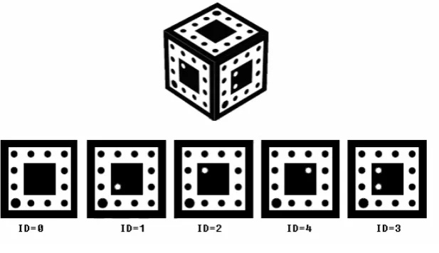
Figure 1: Target under Detection
The primary goal of this thesis is to develop an FPGA based embedded vision
system for recognizing in real time the certain blob pattern shown in figure 1. As an
example, this vision system can be used to track and monitor the process of assembling
nuts on an engine automatically. As we can see from the application scenario shown in
fastening or unfastening the nuts. By identifying the location and orientation of the target,
it is possible to make sure that every nut is mounted correctly. Hence this vision system
can assist by increasing nut assembly accuracy, reducing rework, and thereby increase the
productivity and profitability of the automotive manufacturing process.
Figure 2: Application Scenario
Figure 3: Blob Pattern
As we can see, there are five faces on a target. Each of them has a black square in
face. The ID of each face is determined by the relative position of the origin and the
white dots.
The main focus of this project has been designing hardware architecture and
porting the PC based algorithm to the FPGA system, as well as developing the reusable
Intellectual Property (IP).
1.2 Thesis Organization
The following content is organized as follows. The second chapter provides a
review of the FPGA implementation for image processing, analyzes the features of image
processing algorithms, and explains the advantages as well as the challenges of FPGA
implementation for image recognition. In addition, the general architecture of FPGA
implementation for image identification is developed. Furthermore, the recent advances
and state-of-art FPGA technologies, including embedded CPU integrated with FPGA and
the advanced tools for developing the FPGA system, are introduced. The final part of the
second chapter also describes some existing FPGA-based embedded vision system.
In chapter three, the FPGA based embedded vision system developed in this
thesis is explained. Its hardware architectures, including board level architecture, IP level
architecture as well as circuit level architecture are described first. Here, the architecture
design is focusing on reducing the silicon area and occupying the least resources. Several
reusable IPs are designed and reused in the whole architecture. The usage of each
reusable IP will be explained in depth. Next the proposed recognition algorithm is
related software design is described, including a Windows GUI application and the
firmware running on an embedded CPU (called Microblaze) integrated in FPGA
In the fourth chapter, the experiment results are presented and the related analysis
is explained. During the whole design process, multiple design options are chosen and
then implemented. Their advantages and disadvantages will be addressed and the
experiment results will be explained in detail.
Finally, the fifth chapter presents the conclusion of this thesis as well as the
2 REVIEW OF LITERATURE
2.1 Overview of FPGA Implementation for Image Recognition
Image recognition has been used in a wide range of industrial, commercial,
civilian and military applications for over two decades. Some notable applications
include medical image analysis, public video surveillance, automatic vehicle guidance
and human machine interface. One of the inherent limitations encountered when dealing
with images is the large data size that impedes development of systems for real-time
implementation.
In order to enhance real-time implementation, two aspects of implementation are
endeavoured; one is to optimize algorithm and the other is to adopt a novel hardware
platform. The most popular hardware platform used is the general purpose central
processing unit due to its matured operating system and user-friendly interface. However,
due to increase in image size, data width, interruption of operating system by user
instructions and other regular management real-time application becomes less realizable.
Two possible approaches to enhance the performance of a hardware processor are
to increase the operation frequency and to use parallel operation. For the latter case
research community has already witnessed the adoption of a variety of processors, such
as multi-core CPU, Digital Signal Processors (DSPs), Single Instruction Multiple Data
(SIMD) processor, and Graphics Processing Unit (GPU). These processors are designed
separates storage and signal pathways for instructions and data. This is done to ensure
that both data and instruction can be fetched simultaneously to realize temporal
parallelism. In addition, there are also other components inside DSP to realize parallel
operation such as Multiply and Accumulate (MAC).
Field Programmable Gate Arrays (FPGAs) have emerged decades ago but were
traditionally used for glue logic. With an increase in its logic density, FPGA began to
become a useful parallel platform for image processing. It is made up of a large number
of logic arrays and abundant I/O pads, and forms a general and unspecified logic circuit
ready for custom configuration. FPGA’s advantage relies in its parallel processing
capability, which offers temporal parallelism at the expense of spatial parallelism.
Another significant feature of FPGA is its software like reconfiguration flexibility [2].
Some FPGA novice may think that FPGA’s advantage rests with its super high
operation frequency. Unfortunately, owing to the limitation of its architecture and
manufacture process, contemporary FPGA can only run at a maximum of several
hundred MHz, while a common CPU in our PC can easily reach several Giga Hz clock
frequencies. In terms of operation frequency, FPGA is absolutely a loser.
The reason why FPGA can outperform other processors is that FPGA is a real
parallel processor, for example it will take 5 operation cycles for CPU to finish an
addition: (1) fetch instruction from memory, (2) decode the meaning of fetched
instruction, (3) fetch data from memory, (4) execute addition operation, (5) write the
result back to memory; while for FPGA, it will only take one operation cycle to finish
this operation. If there are 20 addition operations, a CPU will take 100 cycles to finish
simultaneously. Now assuming that the CPU can run at 2GHz clock frequency and each
operation will take only one clock cycle, then to finish 20 additions will cost 0.05s.
Assuming that the operation clock of FPGA is 100MHz, and then it will only take 0.01s
to finish the same 20 operations. Hence it is easy to realize the benefits offered by
FPGA’s parallelism. In particular for operator intensive processing, more significant
improve-ments can be achieved by FPGA compared to serial processors like CPU.
However, not every image processing algorithm is suitable for FPGAs. It is
significant to understand FPGAs’ strength and limitation. The positive side of FPGA has
been addressed above, and the remaining paper will present its negative side. In addition,
some issues of FPGA implementation for image processing will be discussed.
2.2 Algorithm Feature and FPGA Implementation Challenges
Image processing algorithms vary depending on different application, hence
numerous algorithms exist. But they can be classified into two groups:
memory-independent algorithm and memory-dependent algorithm.
Memory-independent algorithms have the following two features enabling it to
perform in a stream-like mode and thus are easy to implement in FPGA.
1) Neighbouring operation.
The so-called Neighbouring operation is popular among many image processing
algorithms, for example, Median Filter, Edge detector (including Sobel, Prewitt,
Laplacian and Gaussian, Canny), Harris Corner detector, and stereo vision algorithms.
incoming pixel stream from a digital camera). In literatures, these algorithms are called
neighbour operation or kernel operation or point operation.
2) One-pass operation.
It means that there are no iterations in the algorithm and image processing can be
done in just one pass. This feature eliminates the demands for storing one whole frame of
image data into memory.
Many neighbouring operators are also one-pass operators but some are not, for
example one basic image processing algorithm called Connected Components Labeling,
also belongs to a neighbouring operator class but it cannot be completed in one pass. In
[3], a single pass connected components algorithm is presented but it is not practical in
real applications since it occupies too many on-chip memories. When it comes to High
Definition (HD) image, off-chip memory is necessary to store image data.
Memory-independent algorithms are suitable for FPGA implementation because it
eliminates the requirement of off-chip memory. Usually, only a small amount of image
data is stored temporarily in the on-chip memory of FPGA for window processing. This
reduces the cost of board components and increases the speed of system so as to realize
real video-rate processing.
On the contrary, memory-dependent algorithms usually require at least two
iterations in operation, and cannot finish operations in one pass. So it has to store
incoming image data into external memory for practical application.
When it comes to memory-dependent algorithms, the limitation of FPGA
a) The introduction of external memory will hinder the speed of the whole system
since the bottleneck lies in the interface between FPGA and the external memory. The
memory bandwidth will determine the overall system performance.
b) Memory-dependent algorithms often concern complicated operation. It may be
relatively easier to develop from the view point of pure software like Matlab or C
language, but it is not always easy to change software into pure hardware [1].
In addition, FPGA has some other issues that should be paid attention to, for
example the difference between fixed point number and floating point number, as well as
the available operations in FPGA. During algorithm development, floating-point numbers
are often used because they represent infinite precision. If the algorithm is to be
implemented in hardware, floating-point numbers are not always feasible. The solution is
to convert very precise floating-point numbers to less precise fixed-point numbers. This
process in Matlab is called quantization. Quantization is an iterative process, and requires
comparing the results of floating-point and fixed-point process, so becomes the most
difficult step for designers. As for available operators, during algorithm development,
there is no limitation on the type of operations. But, it is not true for FPGA development.
Only a limited set of operations can be synthesized, such as addition and deduction.
Arbitrary division and multiplication should be avoided as long as it is possible for the
purpose of saving resources and reducing circuit size.
2.3 System Architecture For Video Rate Image Processing
Real-time image processing is closely related with hardware structure. Assuming
every frame at the speed of camera’s video output, then we say it is a video rate image
processing system.
According to the discussion in section 2, it is apparent that it is relatively easier to
implement memory-independent algorithms in FPGA for video rate processing. Hence,
the following general system architecture is provided for solving this problem.
Figure 4: General Architecture of FPGA Implementation for Image Processing
This figure 4 displays an image acquisition and processing system. Image video is
captured via camera, and then transferred to FPGA for processing and the processed
result is output via output interface. Here, one FPGA and six external memories are
displayed for concept illustration. In real hardware platform, multiple FPGAs can be used,
and the number of external memories can be any number larger than or equal to 2. The
key point of this general architecture is the adoption of multiple independent external
memories, which could work as buffer and assist pipe-line processing or ping-pang
operation. Addition of external Memories will only increase output latency while the
system throughput will remain the same.
Furthermore, no matter how complex the algorithm is, it is still possible to reach
in-stance if the image processing operation will take a period of 1 video frame, we can use
only 2 external memories for video-rate processing. If the processing is too compli-cated
and will take a period of 10 video frames, then we merely increase the number of
memory units to 11. In short, it is always possible to reach video-rate operation at the
expense of extra memories.
Here it should be pointed out that it is possible for multiple circuit blocks to
access one single external memory in a Time Division Multiplexing (TDM) way, which
could get an effect of near-parallel processing. But there are two problems: 1) a memory
controller that can handle multi-port access is needed. This demand will increase the
complexity of FPGA design. Fortunately, current FPGA vender already began to provide
this kind of controller for free, such as the MPMC (Multi-Port Memory Controller)
provided by Xlinx. 2) But another problem cannot be avoided: memory throughput. With
the increase of the problem scale, the throughput of memory will become a bottleneck for
the whole system. Unlike average CPU or DSP, FPGA is a parallel processor by nature. It
is better to use multiple memories so that the potential parallel processing capability of
FPGA could be fully exploited.
2.4 FPGA Based Embedded Processor
In recent years, embedded processors are provided by many FPGA venders in the
form of hard IP existing in silicon fabric or in the form of soft IP which can be
incorporated within FPGA. Figure 4 also shows an embedded CPU inside an FPGA. The
coexistence of an embedded processor and traditional digital logic fabric is to grant the
contradiction between the challenge of FPGA implementation and the system
performance can be compromised since different algorithm fit different platform. The
algorithms suit parallel application can be realized in FPGA logic fabric, while the
algorithm suit serial processor can be realized in embedded CPU inside the FPGA.
The partition of hardware and software can be determined by two factors. One is
the required update time of processing. For example, if one part of a process needs
microsecond or millisecond update time, then it can be processed by software. But if one
part of a process requires 10-100 μs update time, then hardware logic must be exploited
instead of software. The other factor influencing our choice of choosing hardware or
software is the feature of algorithm itself. Only when the algorithm has a large portion
suitable for parallelization, the potential speedup can be achieved by employing FPGA.
Therefore it is necessary to understand every part of the algorithm and make an informed
division between software and hardware.
Table 1 lists part of the contemporary FPGA-based processors [4]. Some of them
exist in silicon as a hard IP, and some can be incorporated within the FPGA as a soft IP.
Table 1: FPGA-Based Processor
Processor name Type/Bits Interface bus FPGA vendor
MicroBlaze Soft/32 IBM Coreconnect Xilinx
NIOS Soft/32 Avalon Altera
LatticeMico32 Soft/32 Wishbone Lattice
CoreMP7 Soft/32 APB Actel
ARM Cortex-M1 Soft/32 AHB Vendor independent
Core8051 Soft/8 Nil Actel
Core8051s Soft/8 APB Actel
PicoBlaze Soft/8 Input/Output ports Xilinx
PowerPC Hard/32 IBM Coreconnect Xilinx
AVR Hard/8 Input/Output ports Atmel
Figure 5: Functional Block Diagram of MicroBlaze Core
In this project, a MicroBlaze embedded processor soft core is adopted. It is a
32-bit Reduced Instruction Set Computer (RISC) optimized in Xilinx FPGA. As a kind of
soft IP, it can be synthesized and incorporated into some particular Xilinx FPGA by using
general logic fabric resources. Figure 5 shows a functional block diagram of the
MicroBlaze core.
Thirty-two 32-bit general purpose registers
32-bit instruction word with three operands and two addressing modes
32-bit address bus
Single issue pipeline
There are dozens of configurable features including optional on-chip bus, optional
data and instruction cache to name a few. This flexible reconfiguration enables the users
to choose their desired set of features according to their design requirements.
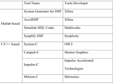
2.5 IP Designed with System-Level Tools
One of the goals of the FPGA design is to ease the transformation from algorithm
to real hardware circuit. In recent years, a number of system-level tools began to emerge.
Table 2 lists some of the system-level tools that have emerged so far.
Table 2: System-Level Algorithm Mapping Tools
Tool Name Tools Developer
System Generator for DSP Xilinx
AccelDSP Xilinx
Simulink HDL Coder Mathworks Matlab based
Synplify DSP Synplicity
System-C OSCI
Catapult-C Mentor Graphics
Impulse-C
Impulse Accelerated
Technologies C/C++ based
DIME-C Nallatech
Handel-C Celoxica
Carte SRC Computers
Streams-C Los Alamos National Laboratory
C/C++ based tools are developed for designing the hardware and the software
simultaneously, and for easing the creation of test benches. Based on this tool a software
programmer are not supposed to understand the hardware in depth, and thereby
expatiating the design process, increasing productivity. To take Impulse-C as an example,
it uses the communicating process programming model to develop highly parallel, mixed
hardware/software algorithms and applications. But as stated in [57], C/C++ language
programming is not a replacement for the existing hardware description languages such
as Verilog HDL and VHDL. It can be used to describe a wide variety of functions that fit
the FPGA hardware, but we cannot expect that it is used to describe a low-level hardware
structures.
Compared to C/C++ based tools, the Matlab based tools have a much shorter
learning curve. While among the Matlab based tools, AccelDSP is more flexible than
others, and therefore is recommended here.
The AccelDSP is a high-level DSP synthesis tool facilitating the mapping from a
Matlab floating-point design to a Xilinx FPGA fixed-point design. It reads and analyzes
the Matlab code and then automatically generates a fixed-point version of Matlab design.
Next, this fixed-point design will be verified, simulated and finally a synthesizable RTL
Every AccelDSP project must have two “.m” files i.e. a script m-file and a
function m-file. The script m-file is used to apply stimulus and plot results whereas the
function m-file is used for realizing the design functions. Certain style of the Matlab
codes are mandatory and the synthesizable Matlab codes must use loops to process every
pixel, and at the same time complicated functions and operations like convolution cannot
be adopted.
The users can decide if the auto-referred data precision is enough; and if not,
users are allowed to manually adjust the model to reduce quantization error. In the flow
of AccelDSP design, this conversion from floating-point to fixed-point is the most critical
and time consuming process.
Compared to hand-coded RTL module, the results of AccelDSP are less efficient
in terms of area and timing. The generated RTL code also lacks readability, making it
difficult to maintain, however, it is still worthwhile to use AccelDSP since it can
dramatically reduce design time.
2.6 Existing FPGA-Based Embedded Vision System
In the past literatures, lots of works have been done to implement the image
recognition algorithms on a FPGA. However, many of them only focus on some simple
ones which can be finished in one pass and do not require the aid of external memories.
For instance, some neighbourhood operations, which typically include median filter,
Sobel, Prewitt, Laplacian, Gaussian, Canny [5, 7] and Harris corner detector as well as
stereo vision algorithms [51], etc. In addition some researchers also exert themselves to
However, many image recognition algorithms are by nature iterative operations
and cannot work without the aid of off-chip memory. For example, one basic image
processing algorithm named the Connected Components Labeling, which also belongs to
neighbourhood operator, cannot be completed in one pass. In [3], a single pass connected
components algorithm is presented, but it is difficult to be used in real applications since
it consumes too many on-chip memories. Optical flow is another example that needs the
introduction of external memory, and a corresponding solution is described in [52], which
unfortunately can only deal with a QVGA-size (320 240) video image.
As a matter of fact, it is better to introduce off-chip memory when implementing
complicated algorithms on FPGA for the purpose of reducing costs and making the
system flexible. One solution described in [55] is a negative example. It requires a bigger
FPGA when dealing with higher resolution images, making it too expensive to affordable
and loosing the expandability.
In recent years, CPU integrated in FPGA enhances the processing capability of
FPGA, and making FPGA a promising platform to develop SOC. [53] describes a
FPGA-based people detection system, which adopts a 32-bit soft processor named the
Microblaze. However, in [53], not only the hardware logic circuit on the FPGA is used,
but also the embedded soft CPU is involved in computation, which jeopardizes the
system performance deeply: only a low system speed of 2.5 frames per second (fps) is
reached. It is hard to be used in real-time application. In [54] another FPGA-based vision
system adopting integrated CPU is described. In this work, all the algorithm operations
the general operation. However, the system only achieves a low speed performance of
processing VGA (640 480) at 10fps.
The following two figures display the FPGA board used in [51] and [54]
respectively. They both adopt Xilinx Virtex-4 series FPGA.
Figure 6: FPGA Board Used in [51]
Figure 7: FPGA Board Used in [54]
a set of complex instructions by the embedded Microblaze CPU to perform the whole
algorithm. By virtue of the hardware parallel architecture, a real-time performance of full
3 DESIGN AND METHODOLOGY
3.1 Board-Level System Architecture
The proposed embedded vision system is capable of acquiring and processing VGA
video to extract the pre-defined object information in real time. Its board-level diagram is
shown in the following figure.
Figure 8: System Architecture Diagram in Board Level
The camera on the left hand side provides FPGA with a raw video stream through the
Image Acquisition port under the control of I2C bus. An external DDR2 memory is
introduced for the algorithm operation, because the algorithm is an iterative process and
requires handling large amount of image data. Through the Multi-Port Memory
Controller (MPMC), and embedded Microblaze CPU and internal digital logic are
connected to external DDR2 memory for fetching and storing data. The peripheral GPIO
is used to control several LEDs on the board so that the internal logic status can be
to display on a Windows Graphic User Interface (GUI) application. A RS232 port is used
to transfer analysis because it consists of only the object ID along with its coordinates,
and occupies a small bandwidth. However, the video stream is another story, consuming
a large amount of bandwidth, so a USB 2.0 is adopted for video transmission.
Figure 9: Functional Block Diagram of OV10121
1) Camera: an omnivision OV10121 Black/White CMOS WVGA High Dynamic Range
(HDR) Camera Sensor is selected. This device incorporates a 768-by-506 image
array capable of operating at up to 30 frames per second. Through the Serial Camera
Control Bus (SCCB) interface, all the camera functions including exposure control,
gain, white balance and windowing, etc., can be programmed. The SCCB is an
updated I2C bus and conforms to the conventional I2C protocol. The most important
feature of this device is its proprietary HDR technology that enables the OV10121 to
making it perform like the human eye under quickly changing lighting conditions.
Figure 9 displays the functional block diagram of OV10121.
2) FPGA: Xilinx Virtex-5 XC5VLX110-FF676 FPGA is adopted. Built on a 65-nm
copper process technology, Virtex-5 FPGAs are a programmable alternative to
custom ASIC technology. It offers a good optional solution for addressing the needs
of performance logic designers, performance DSP designers, and
high-performance embedded systems designers, with unprecedented logic, DSP, hard/soft
microprocessor, and connectivity capabilities. In addition to its huge amount of logic
resources (110,592 logic cells), XC5VLX110 contains many hard-IP system level
blocks, including powerful 36-Kbit block RAM/FIFOs, 550 MHz second-generation
2518 DSP slices, enhanced clock management tiles with integrated DCM (Digital
Clock Managers), phase-locked-loop (PLL) clock generators, and advanced
configuration options. All of these features make XC5VLX110 a good platform to
develop sophisticated image processing algorithms.
Figure 10: Virtex 5 FPGA
Board-level architecture shown in the above subsection only focuses on the
interconnection of components on a board, but does not display the circuit architecture
inside the FPGA. The following figure illustrates the system architecture inside the
FPGA in IP level.
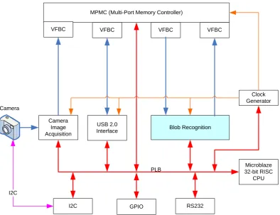
Each square block in Figure 11 represents a circuit unit, and is called an IP. Each
IP can perform a certain function, and is equipped with a uniform interface called PLB so
that each IP can be connected together with Microblaze (the soft-CPU core provided by
Xilinx), to form an integrated system.
Blob Recognition USB 2.0
Interface Camera
Image Acquisition
MPMC (Multi-Port Memory Controller)
VFBC VFBC VFBC VFBC
Camera
Microblaze 32-bit RISC
CPU
RS232
Clock Generator
I2C GPIO
I2C
PLB
Figure 11: System Architecture Diagram In IP Level
Microblaze is a 32-bit RISC CPU soft core, and is integrated here for controlling
development tools including compiler and assemblers are provided by Xilinx to help
the designer code in C or C++.
The PLB is one element of the IBM CoreConnect architecture, and is a
performance synchronous bus designed for connection of processors to
high-performance peripheral devices. The PLB includes multiple advanced features
concerning its data transfer, bandwidth usage, pipeline architecture, bus arbitration,
and memory guard methodology to name a few. Most of these features map well to
the FPGA architecture, however, some can result in the inefficient use of FPGA
resources or can lower system clock rates. As a result, Xilinx uses an efficient subset
of the PLB for Xilinx-developed PLB devices.
The Clock Generator is an IP provided by Xilinx, and is responsible for providing
clocks for every other IP according to system wide clock requirements.
MPMC stands for Multi-Port Memory Controller, and is used to access external
DDR2 memory. It is a fully parameterizable memory controller that supports
SDRAM/DDR/DDR2/DDR3/LPDDR memory. In addition, MPMC provides access
to memory for one to eight ports.
VFBC stands for Video Frame Buffer Controller, and is a connection layer between
each IP and the MPMC. It provides each IP with access to external DDR2 memory,
and allows IPs to read and write data in two dimensional (2D) sets regardless of the
size or the organization of external memory transactions. The VFBC includes
separate Asynchronous FIFO interfaces for command input, write data input, and
read data output. This is useful to decouple the video IP from the memory clock
GPIO stands for general purpose I/O, and is a port to control some external LEDs for
indicating the system status.
RS232 is a serial communication port to communicate with a computer for receiving
instructions and outputting results.
Image Acquisition is a video timing generator to match the video output port of an
Omnivision camera, and then capture its generated video stream.
I2C is a 2-wire bus to write/read the registers of an Omnivision camera OV10121,
thereby controlling its operation mode. Omnivision uses an updated I2C bus
interface called Serial Camera Control Bus (SCCB) interface, which conforms to the
protocol of conventional I2C bus interface.
USB stands for Universal Serial Bus, and is used in this project to communicate with
a computer for receiving instructions from user and outputting video stream to a
computer for display. This USB IP is designed to interface with an on-board Cypress
EZ-USB FX2™ USB Microcontroller. The EZ-USB FX2 device is a single-chip
integrated USB 2.0 transceiver, Serial Interface Engine (SIE) and 8051
microcontroller. This device supports full-speed (12 Mbps) and high-speed (480
Mbps) modes. The FX2 interface to the Virtex-5 FPGA is a programmable state
machine that supports 8- or 16-bit parallel data transfers. The USB FX2 device is
used in a slave mode where the FPGA accesses the FX2 like a FIFO.
Blob Recognition is the IP handling the blob recognition algorithm. The embedded
algorithm is iterative by nature and operates a large amount of data. So two VFBCs
are adopted here to ease the operation of the frequent fetching of data from an
Among all of these IPs, four of them, including Image Acquisition, I2C, USB and
Blob Recognition, are designed by the author. In the following subsections, the design of
these four IPs will be addressed.
3.3 Peripheral IP Design
3.3.1 Image Acquisition IP
Image Acquisition IP is a video timing generator to match the video output port of
Omnivision OV10121 camera, so that the generated video stream can be captured and
stored in an external DDR2 memory through the FPGA. The related input and output
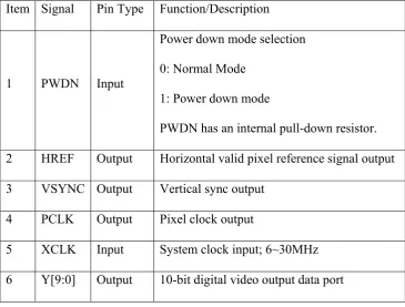
pins of the OV10121 are listed in Table 3.
Table 3: Pin of OV10121 Digital Video Interface
Item Signal Pin Type Function/Description
1 PWDN Input
Power down mode selection
0: Normal Mode
1: Power down mode
PWDN has an internal pull-down resistor.
2 HREF Output Horizontal valid pixel reference signal output
3 VSYNC Output Vertical sync output
4 PCLK Output Pixel clock output
5 XCLK Input System clock input; 6~30MHz
6 Y[9:0] Output 10-bit digital video output data port
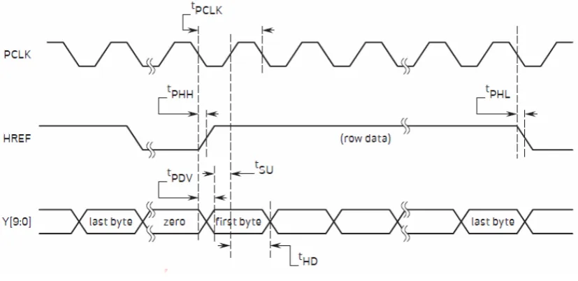
Figure 12: Horizontal Timing
Figure 13: VGA Frame Timing
The Image Acquisition IP can be divided into three parts. The first is a timing
generator called an Image Capture Interface. It is used to generate the two inputs of the
OV10121, XCLK and PWDN, and also receives the incoming 10-bit digital video stream
Y[9:0] according to the timing of PCLK, HREF and VSYNC. The second part is called
Video to VFBC, and is used for transferring the captured video stream to an external
IP to a PLB bus so that it can be under the control of the Microblaze. The following is the
functional diagram of Image Acquisition IP.
Figure 14: Image Acquisition IP Functional Diagram
3.3.2 I2C IP
The Omnivision OV10121 camera uses an updated version of the I2C bus
interface called Serial Camera Control Bus (SCCB) interface, which conforms to the
protocol of the conventional I2C bus interface.
The I2C bus is a popular serial, two-wire interface used in many systems because
of its low overhead. The two-wire interface minimizes interconnections so ICs have
fewer pins, and the number of traces required on printed circuit boards is reduced.
Capable of 100 KHz or 400 KHz operations, each device connected to the bus is software
addressable by a unique address with a simple Master/Slave protocol.
The I2C bus consists of two wires, a serial data (SDA) and serial clock (SCL),
which carry information between the devices connected to the bus. The number of
devices connected to the same bus is limited only by a maximum bus capacitance of 400
pF. Both the SDA and SCL lines are bidirectional lines, connected to a positive supply
of devices connected to the bus must have an open-drain or open-collector in order to
perform the wired-AND function.
Each device on the bus has a unique address and can operate as either a
transmitter or receiver. In addition, devices can also be configured as Masters or Slaves.
A Master is the device which initiates a data transfer on the bus and generates the clock
signals to permit that transfer. Any other device that is being addressed is considered a
Slave. The I2C protocol defines an arbitration procedure that insures that if more than
one Master simultaneously tries to control the bus, only one is allowed to do so and the
message is not corrupted. The arbitration and clock synchronization procedures defined
in the I2C specification are supported in this project.
Data transfers on the I2C bus are initiated with a START condition and are
terminated with a STOP condition. Normal data on the SDA line must be stable during
the High period of the clock. The High or Low state of the data line can only change
when SCL is Low. The START condition is a unique case and is defined by a
High-to-Low transition on the SDA line, while the SCL is High. Likewise, the STOP condition is
a unique case and is defined by a Low-to-High transition on the SDA line, while the SCL
is High. The definitions of data, START and STOP, insure that the START and STOP
In this thesis, a custom I2C IP is designed and has the following specifications:
Only supports master operation. Does not support slave mode.
Supports multiple-master operation
Supports I2C WAIT state (I2C clock line SCL is held LOW by external
devices)
Only supports byte write/read, and does not support page write and sequential
read
Data transfer format is seven-bit address format
The PLB controller interface
400KHz Operation since the Omnivision OV10121 camera sensor requires
400Khz operation.
The following figure displays the diagram of the designed I2C IP. It can be
divided into two major blocks, the PLB interface and the I2C controller. The PLB
interface is for connecting the I2C controller to Microblaze through a PLB bus, and the
I2C controller is for generating the I2C signal timing conforming to the I2C protocol.
Figure 16: Block Diagram of I2C Master Controller
The I2C bus interface logic consists of several different processes.
Generation of SCL, SDA, START and STOP Conditions is to generate the
SCL and SDA signal outputs on the I2C bus when in Master mode.
Start/Stop Detection is to monitor Start/Stop conditions on the I2C bus.
I2C State Machine contains two state machines: Main State Machine and
One-Bit State Machine. The first one is responsible for the whole flow of the
I2C controller, while the latter one is responsible for generating one bit.
3.3.3 USB IP
USB stands for Universal Serial Bus, and is used in this thesis to communicate
with a computer for receiving instructions and outputting video stream to display. This
USB IP is designed to interface with an on-board Cypress EZ-USB FX2 USB
Microcontroller CY7C68013A. The EZ-USB FX2 device is a single-chip integrated USB
2.0 transceiver, Serial Interface Engine (SIE) and 8051 microcontroller. This device
supports full-speed (12 Mbps) and high-speed (480 Mbps) modes. The FX2 interface to
the Virtex-5 FPGA is a programmable state machine that supports 8 or 16-bit parallel
data transfers. The USB FX2 device is used in a slave mode where the FPGA accesses
the FX2 like a FIFO.
USB development requires the knowledge of both developing a Windows
Operation System based application and designing embedded systems, and requires
mastering high-level protocol and low-level circuit design, which is a very complicated
process. In this thesis, the FPGA based glue logic to interface the CY7C68013A is
designed. In addition, with the aid of the development suit provided by Cypress, a
operation of the FPGA system. In this subsection, only the logic design of the USB
interface will be addressed.
Figure 17 displays the diagram of the designed USB interface IP. It can be
divided into three major blocks:
FIFO Controller generates the Cypress defined slave FIFO signal timing to
interface with the on-board Cypress USB controller.
PLB interface connects the USB IP to the Microblaze through a PLB bus.
USB To VFBC transfers the video data stored in an external memory to a
computer via a VFBC port.
EZ-USB Slave Mode PLB Interface IFCLK FIFO Controller FLAGA FLAGB FLAGC FLAGD/SLCS# SLOE SLRD SLWR PKTEND FD[15:0] FIFOADR[1:0] Microblaze PLB Bus USB IP
USB to VFBC
MPMC (Multi-Port Memory Controller) V F B C DDR2 Memory
Figure 17: Interface between Slave mode EZ-USB and FPGA USB IP
The on-board Cypress EZ-USB FX2 USB Microcontroller is configured to work
in slave mode, and is controlled by an external master: the FPGA. FPGA accesses it like
a 16-bit FIFO.
The USB Interface logic inside the FPGA accesses the FIFOs through an 8 or
16-bit wide data bus, FD[15:0]. The data bus is bidirectional, with its output
Slave-mode EZ-USB FX2 contains four slave FIFIOs. The FIFOADR[1:0]
pins select which of the four FIFOs are connected to the FD bus and which
are controlled by the FPGA.
In asynchronous mode (IFCONFIG.3 = 1), SLRD and SLWR are read and
write strobes; in synchronous mode (IFCONFIG.3 =0), SLRD and SLWR
work as enable signals. In this project, synchronous mode is adopted.
The slave FIFO interface can be clocked from either an internal or an external
source. In this thesis, the internal clock source is adopted and is also
configured to output on the interface clock (IFCLK) pin to clock the USB
Interface logic inside the FPGA. In this way, the FPGA logic design is
simplified.
Figure 18: USB Slave FIFO Synchronous Timing Models
Four pins — FLAGA, FLAGB, FLAGC, and FLAGD— are adopted to
indicate the status of the EZ-USB’s FIFOs: ‘FIFO full’ or ‘FIFO empty’.
PKTEND is asserted by the FPGA to commit an IN packet to the USB
regardless of the packet’s length. Usually it used when the master wishes to
send a ‘short’ packet.
into two state machines: one is for writing the slave FIFO, and the other is for reading the
slave FIFO. These two state machines will have a similar operation process, so only the
FIFO write state machine is shown below as an example.
Figure 19: State Machine of Synchronous FIFO Writes
3.4 Core Algorithm IP Design
Blob Recognition IP is just the circuit block that contains the core algorithm to
search and identify the target. In the following subsections, this algorithm will be
explained from the viewpoint of software at first, and then the FPGA implementation will
be addressed.
3.4.1 Blob Recognition Algorithm
The proposed blob recognition algorithm is aiming at processing a gray-scale
image in VGA size, and can be divided into three major steps as below:
Image scale down: the incoming video stream is in VGA (640x480) size. In
order to decrease the processing time and to reduce the resources for
computation, this incoming VGA video image is downscaled by factors of
Candidate location: given a downscaled QQVGA image in which the position
of the target is unknown, this step is supposed to search for every possible
candidate. Multiple candidates may be chosen according to a certain criterion,
which exerts strong influence upon the performance of the whole system.
Image Down Scale (From VGA
to QQVGA) Blob Candidate Localization Yes Normalization of Candidate Image Block Binarization Gaussian Smoothing Binarization Gaussian Smoothing Recognitio of face ID Blob Recognition
Is blob found? Candidates
Search and store
Is candidate available? Output Results Yes No No
Figure 20: Flow Chart of Proposed Algorithm
Object identification: given each candidate, the related image data will be
captured from the main memory to process and analyze. An identification
algorithm inspired by the unique feature of the blob face is adopted to extract
The latter two steps can be divided into finer processes, and are illustrated in
Figure 20.
3.4.1.1 Gaussian Smoothing
The Gaussian Smoothing is used to blur the image under detection for further
processing. Each pixel is replaced with a weighted average of its neighbourhood when
the mask is sliding over the image. It belongs to the neighborhood operation (or is called
a pixel operation or a kernel operation), and is a kind of widly used image processing
filter defined by the following equation.
2 2 2 ) ( ) , ( y x Ke y x g
, ( 1 )
where, (0, 0) is the center of the mask, and determines how fast the weight
decay. Usually, the sum of the mask coefficients is 1. The selected Gaussian mask is
shown in Figure 21.
1 4 7 4 1
4 16 26 16 4
7 26 41 26 7
4 16 26 16 4
1 4 7 4 1
Figure 21: 5-by-5 Gaussian Kernel
It is worthwhile to notice the parameters inside the mask since they are all
selected carefully for the purpose of simplifying computation and reducing logic
resources. In this Gaussian kernel, only three parameters, 7, 26 and 41, need the
of two only involves a logic shift. Taking the parameter 4 as an example, to shift left by
two bits on a number has the same effect of multiplying it by 4.
3.4.1.2 Binarization
1 1 1 1 1 1 1 1 1 1 1
1 1 1 1 1 1 1 1 1 1 1
1 1 1 1 1 1 1 1 1 1 1
1 1 1 1 1 1 1 1 1 1 1
1 1 1 1 1 1 1 1 1 1 1
1 1 1 1 1 1 1 1 1 1 1
1 1 1 1 1 1 1 1 1 1 1
1 1 1 1 1 1 1 1 1 1
1 1 1 1 1 1 1 1 1 1 1
1 1 1 1 1 1 1 1 1 1 1
1 1 1 1 1 1 1 1 1 1 1
Figure 22: 11-by-11 Average Kernels
Binarization is to binarize the gray-scale image under detection. In the literature,
there are many algorithms about binarization, such as the Otsu method. The Otsu method
is a kind of global threshold method, and is sensitive to abrupt change of lighting
conditions. So researchers turn to adaptive binarization algorithms focusing on local
threshold. When it comes to different applications, different binarization methods are
used. In this project, based on the size of the image under detection, the specific blob
based adaptive threshold method is adopted. The kernel of this average filter is 11-by-11
in size, and is shown in Figure 22.
Each pixel is replaced with ‘1’ or ‘0’ according to the following equation when
the mask is sliding over the image. Where, ‘1’ represents white pixel, and ‘0’
represents a black pixel,
Delta avg Int Int if Delta avg Int Int if BW _ ) 0 , 0 ( _ ) 0 , 0 ( 0 1 ) 0 , 0
( , ( 2 )
where, (0, 0) is the center of the mask, and BW(0,0) is the value that is going to
be assigned to the center pixel of the mask; Int(0,0) represents the current intensity
value of the center pixel, and the Int_avg is the average intensity value of the
neighbourhood; Delta is a parameter determining the threshold.
QQVGA
Smoothed QQVGA after Gaussian kernel
Binarized QQVGA after adaptive threshold
the black heart block in a face can be correctly segmented from its background, which is
just the key to successfully selecting a target candidate. Figure 23 shows an example of
the results of these two steps.
3.4.1.3 Candidates Search and Store
This step tries to find all the sub-images that contain an object and then stores into
memory the coordinates and the size of the selected sub-images (candidates). In order to
search for the possible candidates, the following method is proposed: given a binarized
image, each component is grouped and labelled by using a Connected Component
Labelling (CCL) method, and then the dimension of each component is measured,
including maximum x axis, maximum y axis, minimum x axis, minimum y axis and
center of the component. It is expected to choose all the possible candidates according to
this simple measurement and some certain criterion, for example the ratio of width and
height and the distance between the center of the component to the border of the image.
CCL scans an image and groups its pixels into components based on pixel
connectivity. But the traditional CCL can only handle one single type of pixel at a time,
either black or white. In this project both black and white components are taken into
consideration, hence the following Dual Connected Component Labeling (DCCL)
method is proposed.
Similar to the conventional CCL method described in [50], DCCL also adopts a
23 mask and an equivalent table.
23 mask: the connectivity of each pixel is checked when a 23 window is
sliding across an image, where the 23 window is shown below. “A” is the
Equivalent table: it is used to store the label values that actually belong to
one single component.
Figure 24: 2x3 Mask of DCCL
However, unlike the conventional CCL method, DCCL changes the data structure
and adopts another equivalent table called a BW_EQ table for storing the information of
connectivity between different types of pixels.
Data structure: In the 23 mask, each pixel is represented by an N-bit data.
(N-1 downto 1) bits represent label value.
Nth bit indicates the type of pixel: 1 ->black, 0 ->white.
For example:
B(N) = 1 indicates that pixel B is a pixel in black color.
B(N-1 downto 1) = 3 indicates that B is labelled number 3.
BW_EQ table: an equivalent table that stores the information of connectivity
between black and white components.
Each DCCL processing will be done according to the following order: E -> D ->
C -> B. A is the pixel under detection.
Label Assignment: starting from pixel E, it searches the first pixel which has
the same Nth bit as that of pixel A, and also has a non-zero label value. If
found, then its label is assigned to pixel A. Or if not found, a new label is
Equivalent Table: after the label assignment, label comparison continues
between A and other pixels with the same Nth bit. If different labels are
found, the labels are stored into equivalent table.
BW_EQ Table: it finds all the pixels with a different Nth bit from that of A,
and then store the labels into the BW_EQ table.
After black and white components are grouped and labelled by the DCCL method,
the dimension of each labelled component will be measured for the purpose of selecting
target candidates. In this thesis, based on the measured size of the segmented heart block,
it is possible to estimate the size of the candidate image block, since there is a certain
geometric relationship between the blobs inside a face: the heart block is a square shape
and the length of its side is almost one third of the length of the side of the square bound.
This relationship is shown in Figure 25.
D
Figure 25: Geometric Relationship of Blob Face
Finally, the coordinates and the dimension information of all the chosen
candidates are stored in a buffer for further processing one by one.
3.4.1.4 Normalization of Candidate Image Block
Every candidate image may have different image sizes. It is helpful for the next
the normalization size is 96-by-96. However, owing to the limitation of the FPGA
memory interface, only the transformation listed in Table 4 is adopted.
Image normalization scales an image to a certain size. It is a popular image
processing operation. In this project, a traditional bilinear interpolation method is adopted:
the incoming image data comes through a filter, and the output pixel value of the filter is
a weighted average of pixels in the nearest 2-by-2 neighbourhood. Figure 26 is an
example of normalization from 128-by-128 to 96-by-96.
Table 4: Normalization List
96x96 -> 96x96 256x256 -> 96x96 384x384 -> 96x96
128x128 -> 96x96 288x288 -> 96x96 416x416 -> 96x96
160x160 -> 96x96 320x320 -> 96x96 448x448 -> 96x96
192x192 -> 96x96 352x352 -> 96x96 480x480 -> 96x96
224x224 -> 96x96
Figure 26: Normalization from 128-by-128 to 96-by-96
3.4.1.5 Recognition of Face ID
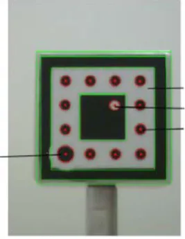
The target is a cube, and has 5 faces with different blob patterns in black and
white. These blob patterns look like nested squares. From Figure 27, it can be seen that
surrounded by 12 small black dots, while the 12 black dots are bounded by another black
square border again.
Among the 12 black dots, the largest one is defined as the origin of the face. The
relative position between the origin and the white dots inside the heart block determines
the ID of the face. In this project, up to four white dots may be located inside the heart
block, and the face ID is calculated by the following equation,
3 2
1
0 2*2 3*2 4*2
2 *
1 W W W
W
ID , ( 3 )
where, Wx = 1 only if a white dot appears on the position of Px (x=1 or 2 or 3 or
4). Position Px is determined based on the relative position between the corner of the
heart block and the origin in a clock-wise direction.
Figure 28 gives examples of face ID. Where, up to 2 white dots exist inside the
heart block.
An intuitive ID recognition algorithm inspired by the feature of the blob face is
proposed. The whole flow chart is illustrated in Figure 29.
Is heart block found? Find the heart
block
Find the white frame
Find all the white dots inside the
heart block Is the white
frame found?
Are there 12 black dots? Find all the black
dots inside the white frame
Count Face ID Yes Yes Yes No No No
Output Face ID Output No
Face ID
End
Figure 29: Recognition of Face ID
1) Find out the heart block: every face has a heart block in square shape. Since
the candidate image block is located based on the segmented heart block, the
In addition, we introduce a bias parameter for the tolerance of the possible
mismatch caused by image distortion or previous image processing.
2) Find out the white frame: two features are helpful to find the white frame: 1)
The central coordinates of the white frame should be very close to the center
of the heart block; 2) The white frame is surrounding the heart block. The
purpose of obtaining the white frame is to search for the 12 black dots
surrounding the heart block.
3) Find out 12 black dots surrounding the heart block: as mentioned before, the
connectivity information between black and white components can be
achieved through DCCL method, and is stored in BW_EQ table. Combining
the information of white frame and the BW_EQ table, the black dots can be
easily screened out.
4) Find all the white dots inside the heart block: with the aid of BW_EQ table
and the measured geometric dimension of each labelled component, it is easy
to get all the white dots. These white dots are used to calculate the ID of the
face.
5) Count face ID: given the information of all the black dots and the white dots,
it is possible to calculate the ID of a face. However, in order to make sure the
position of the origin of the face as well as the position of the white dots
inside the heart block, a fine division of the blob face is illustrated in Figure
![Figure 7: FPGA Board Used in [54]](https://thumb-us.123doks.com/thumbv2/123dok_us/1449232.1177551/34.595.113.522.228.444/figure-fpga-board-used-in.webp)