ABSTRACT
CAO, WEI. Design of Temperature Sensors for Validation of Aseptic Food Processing. (Under the direction of Professor Paul D. Franzon).
With the increasing consumer demands for convenient, high quality, and healthy foods, aseptic processing was proposed as a potential option to meet these demands. In order to validate such a system and also make the process relatively inexpensive, researchers have to find out the “critical particle” in the processing system and determine its time-temperature history. The objective of this work is to develop and validate low power sensors that can be applied to monitor the internal temperature of particulates, as they flow through the heating, holding, and cooling sections of an aseptic processing system. The significance of this study lies in the development of a validated tool and technique that can be used to facilitate validating aseptic processing of multiphase foods and thereby provide the health-conscious consumer with a high quality food product.
Design of Temperature Sensors for Validation of Aseptic Food Processing
by Wei Cao
A thesis submitted to the Graduate Faculty of North Carolina State University
In partial fulfillment of the Requirements for the degree of
Master of Science
Electrical Engineering
Raleigh, North Carolina 2008
APPROVED BY:
_______________________________ ______________________________ Dr. Paul D. Franzon Dr. Kevin Gard
Committee Chair
DEDICATION
BIOGRAPHY
ACKNOWLEDGMENTS
I would like to express my sincere gratitude and thanks to my advisor, Dr. Paul Franzon, for his gracious support and continuous encouragement throughout my graduate study at the North Carolina State University. This thesis could not have been succeeded without his spirited guidance. I have learned innumerable lessons and insights from him on the workings of scientific research in general.
I also want to thank my committee members, Dr. K.P. Sandeep and Dr. Kevin Gard, for providing many valuable comments and suggestions that are essentially necessary for completion of this thesis.
Special acknowledgements are extended to Dr. Steve Lipa for his knowledgeable and valuable guidance, comments and suggestions to this work, and Mr. Harry Reinitz for the device packaging and testing. I would also like to thank all our research group colleagues for their valuable discussion, technical support, and other important contributions.
TABLE OF CONTENTS
LIST OF TABLES ………...………. vi
LIST OF FIGURES ……….……….
vii
CHAPTER 1 INTRODUCTION ………...………..
1
CHAPTER 2 PROJECT OVERVIEW ……….………... 6
CHAPTER 3 OFF-THE-SHELF SENSOR DESIGN ………...….
17
CHAPTER 4 OFF-THE-SHELF SENSOR TESTING AND VERIFICATION ….… 36 CHAPTER 5 CMOS SENSOR DESIGN ..……….. 50
CHAPTER 6 CONCLUSION AND FUTURE WORK ...………... 64
LIST OF TABLES
Table 2.1 Different remote temperature sensors………. 8
Table 2.2 Different external (non-invasive) temperature sensors………... 8
Table 2.3 Different internal temperature sensors……… 8
Table 2.4 Inaccuracy of available temperature sensors in lab……… 10
Table 3.1 List of potential candidate microcontrollers with specification……….… 19
Table 3.2 List of potential candidate batteries with specification………. 19
Table 3.3 List of potential temperature sensors with specification……… 21
Table 3.4 List of potential SRAM memory chips with specification………. 22
Table 3.5 List of potential FLASH memory chips with specification…….……….. 22
Table 3.6 Complete component list………... 23
Table 3.7 BR1225A specification……….. 26
Table 4.1 Density calculation of off-the-shelf sensor packages……….… 39
Table 4.2 ADC test results.………
41
Table 4.3 Other possible components……….49
LIST OF FIGURES
Figure 3.1 Typical DCOx range and RSELx steps vs. fDCO………24
Figure 3.2 DCO frequency vs. temperature………..……….. 25
Figure 3.3 Active mode current vs. VCC, TA, and fDCO……….26
Figure 3.4 BR1225A temperature characteristics………... 27
Figure 3.5 Signal connections for 2-wire spy-bi-wire communication………...28
Figure 3.6 System schematic of our temperature sensor……… 30
Figure 3.7 PCB layout of our temperature sensor………...31
Figure 3.8 Off-the-shelf temperature sensor………..…….… 31
Figure 3.9 On-board programming setup………...………. 32
Figure 4.1 Prepare the polypropylene hemispheres………37
Figure 4.2 Sensor packaged in ¾”spheres……….. 37
Figure 4.3 Experiment setup for the batch validation studies………. 38
Figure 4.4 A sensor packaged in 1” sphere……….……… 39
Figure 4.5 A mild temperature test………. 42
Figure 4.6 Temperature variations……….. 43
Figure 4.7 High temperature test results………. 44
Figure 4.8 Temperature variations……….. 45
Figure 4.9 Temperature reading after filtering………... 45
Figure 4.10 High temperature test results………... 46
Figure 4.12 Temperature test results (zoomed in)……….. 47
Figure 4.13 Temperature test at low sampling rate………. 48
Figure 5.1 Scheme of CMOS temperature sensor design………... 53
Figure 5.2 Schematic of temperature sensor and frequency converter………... 54
Figure 5.3 Waveforms of differential comparator……….. 55
Figure 5.4 Schematic of internal clock………... 56
Figure 5.5 Block diagram of digital control unit……… 58
Figure 5.6 Frequency output versus ambient temperature………. 59
Figure 5.7 ASIC circuit waveforms………... 60
Figure 5.8 Detailed ASIC circuit output waveforms……….…. 60
Figure 5.9 Layout of the clock and the temperature sensor………61
Figure 5.10 Layout of the digital control unit………. 62
Figure 6.1 CMOS sensor with simple RF receiver………...69
CHAPTER 1
Introduction
Food safety is rapidly becoming one of the most critically important issues in food industry. The quantitative measurement of the thermal process impact in terms of food safety and quality is essential in relation to the shelf life and acceptability (market and legal) of the product as well as for process optimization and control [1]. The objective of this project is to develop and validate low-power and high-performance sensors that can be applied to monitor the internal temperature of particulates, as they flow through the heating, holding, and cooling sections of an aseptic processing system.
1.1 Project Background and Motivation
techniques and mathematical modeling of the process that every part of the food product receives adequate heat treatment to ensure commercial sterility [3].
In an attempt to address this problem, a workshop was organized by the Center for Advanced Processing and Packaging Studies (CAPPS) and the National Center for Food Safety and Technology (NCFST) in 1995 and 1996 [4]. The conclusions from the workshop were that determination of the residence time distribution (RTD) of at least 299 particulates in the product, determination of the heat transfer coefficient between the particulates and the fluid, and mathematical modeling are vital in process validation. To develop such kind of validation systems, the first and most important factor is the cost and time involved in the extensive process, which is partly due to the necessity to determine the RTD of 299 particles and the heat transfer coefficient between particles and the fluid [5]. This necessity arises due to the fact that we are currently unable to measure the time-temperature history at the “critical point” within particulates as they flow through the processing system [6]. Tetra Pak
of a reliable tool to validate their process and at the same time ensure a high product quality. The sensor system and validation protocol to be developed in this study will serve as that tool.
Generally speaking, “critical point” is the slowest heating portion of the product. For a food product containing only one type of particle, this is the center of the fastest moving particle. However, for a food product containing several types of particles, the “critical point” is the center of the slowest heating particle which may not necessarily be the fastest particle in the system. Thus, if we are able to determine the “critical particle” in a system and determine its time-temperature history, it would tremendously simplify the validation process and make the process relatively inexpensive.
paramagnetic implants within particles [18], ultrasonic tomography [19], micro-thermometry [20], change in proton precession frequency [21], magnetic resonance imaging [22], chemi-luminescent implants [23], thermo-magnetic switch implants [24], and fiber optic sensors [25]. However, all of these techniques are either expensive, elaborate, or difficult to incorporate in an aseptic processing system, or not accurate enough for process validation.
The significance of this study thus lies in the development of a validated tool and technique that can be used to facilitate validating aseptic processing of multiphase foods and thereby provide the health-conscious consumer with a high quality food product. It will pave the way for the development of new food products that were hitherto not developed due to the potentially low quality of the food (as a result of the inherent over-processing in the conventional retort process) in the absence of the tool to be developed in this study. Beyond that this sensor will also be useful in improving the quality of various thermal processes where accurate real-time temperature readings can minimize over-processing. It can also be used in some of the applications where time-temperature integrators are used to monitor the quality and safety of foods.
1.2 Thesis Overview
CHAPTER 2
Project Overview
Temperature is one of the most widely measured phenomena in the process control environment. In this chapter, a detailed review of different types of existing temperature sensing techniques in aseptic food processing is presented, followed by a short discussion on temperature sensor calibration. The previous related development of temperature sensors in the Department of Food Science at NCSU is summarized in Section 2.3. The project objectives, design flow, as well as verification plan, are presented in Section 2.4.
2.1 Temperature Sensing Techniques Review
types of temperature sensors that use various technologies and have different characteristics [8-26]. Many common elements such as resistance temperature detectors (RTDs), thermistors, thermocouples or diodes, as well as some newly developed sensing methods using infrared, microwave, optical or biological techniques, have been used to measure absolute temperatures or temperature changes in various applications. It is maybe worth pointing out that noticeable difference exists between different temperature sensor or temperature measurement device types.
Food scientists and researchers have worked more than a decade attempting to determine the internal temperatures of food particles during continuous flow. The methods that they have used can be roughly classified into two groups: non-contact temperature sensors and contact sensors. The former are also called remote temperature sensors, and the latter could be further divided into two categories: external temperature sensors and internal temperature sensors. They are summarized in the Table 2.1, Table 2.2, and Table 2.3.
Table 2.1: Different remote temperature sensors.
Type Working Principle Comments
Temp sensor using external magnetic flux
Output resonant frequency changes with temperature
No power supply needed for sensor; accurate; relatively simple structure Microwave temp
sensor
Use X-band radiometer
Work in bad environment; more accurate than infrared sensors Infrared temp sensor Detect energy
emitted by target
Only use 0.7-14 micron band Optical fiber sensor Work at high temperature; high
resolution
Table 2.2: Different external (non-invasive) temperature sensors.
Type Working Principle Comments
Pt thermal sensor/heater
Easy to fabricate, calibrate and use; working as both heater and sensor
External sensor on the outer wall
Measure inside fluid temperature by
converting the readings from external sensor
Able to calculate internal fluid temperature with external sensors, when insertion of a thermometer is impossible or impractical
Table 2.3: Different internal temperature sensors.
Type Working Principle Comments
CMOS/bipolar temp sensor
Extremely small and low power; will be discussed in chapter 4&5 Time-temperature
integrator
Use enzyme system or peroxides immobilized on porous glass
Melting point indicators
Color change Able to measure the temperature inside of a particle
Liquid crystal temp sensor
Color change Have to coat liquid crystal on monitored particle
Moving thermocouple
a classic, widely used method; motor-driven thermocouple moving along the tube Temperature
mapping (magnetic resonance imaging)
2.2 Temperature Sensor Calibration
One key secret to high quality temperature measurement results is to have a careful calibration before any tests. Without reliable calibration, the results will always be questionable and hardly worth the effort and cost. Uncertainties result from various factors, including: sensor tolerances, which are usually specified according to published standards and manufacturers specifications; instrumentation (measurement) inaccuracies, again specified in manufacturers specifications; drift in the characteristics of the sensor due to temperature cycling and ageing; possible thermal effects resulting from the installation, for example thermal voltages created at interconnection junctions. A combination of such factors will constitute overall system uncertainty [26].
Temperature sensor calibration provides a means of quantifying uncertainties in temperature measurement in order to optimize sensor and/or system accuracies. It is achieved by elevating the temperature sensor to a known, controlled temperature and measuring the corresponding change in its associated electrical parameter (voltage or resistance). If the sensor is connected to a measuring instrument, the sensor and instrument combination can be effectively calibrated by this technique [27].
at multiple temperature points. Then plug in the recorded data to the function below and determine values for A and B.
T =A1*V +B1 (1) where T is the known temperature, V is the recorded voltage output of the temperature sensor, A and B are constants to be determined.
As a result, we can get the following equation:
+ = + = + = + = 4 * 4 3 * 3 2 * 2 1 * 1 B V A T B V A T B V A T B V A T
where T is the temperature we want to get, V is the recorded voltage output of the temperature sensor, A1-A4 and B1-B4 are known constants.
Table 2.4 shows the inaccuracy of available temperature sensors in our lab.
Table 2.4: Inaccuracy of available temperature sensors in lab.
Name Inaccuracy Comments
LM94021 temp
sensor +/- 2.71 °C Handheld digital
thermometer +/- 0.89 °C
Easy to use; hard to keep a long-time record
Data acquisition
unit +/- 1.25 °C
Very flexible; provide digital output of temperature history
So as a starting point, we should use either the handheld digital thermometer or the data acquisition unit to calibrate the temperature sensors. To further increase the sensor accuracy,
where 0.2 > V ≥ 0; where 0.4 > V ≥ 0.2; where 0.6 > V ≥ 0.4; where V ≥ 0.6;
we might adopt a secondary standards system for high quality comparison and fixed point measurements which would provide accuracies generally between 0.1°C and 0.01°C.
2.3 Previous Work on Temperature Sensing in Department of Food Science
Several sensors have been developed in the Department of Food Science at NCSU in the past few years that can be used to determine the time-temperature history within simulated, conservatively constructed implant-carrier particles.
thermal treatment. Therefore, we have to ensure that the entire particle of our temperature sensor is nearly neutrally buoyant with water and thus exhibits conservative flow behavior.
2.4 Project Overview
The current study will be undertaken with the goal of providing a reliable and quick way to determine the temperature at the “critical point” within an aseptic processing system to facilitate process validation. The technique will involve the development of sensors that can be used to determine the internal temperature of food particles as they flow through the heating, holding, and cooling sections of an aseptic processing system. The sensor will then be implanted in the cavity of a “conservatively” designed carrier particle such that the thermal treatment delivered to the center of this particle will always be less than that received by every other particle in the real food product.
2.4.1 Project Requirements
Listed below are the specific requirements and/or preferences of the temperature sensors in this project:
a. Low power consumption (a very critical issue due to battery duration requirement; ideally in the order of 1mW or less);
b. Small volume (ideally 8mm x 8mm x 8mm or less; must fits in the target package), which can also be interpreted as a low need of gates if we use CMOS sensor;
water);
d. Easy calibration (which means it only needs one or two point calibration; curvature correction to be used only if necessary);
e. Favorably digital output signal (easy to interface with built-in memory chip as well as RF circuit);
f. A temperature range of 25-125 (or 0-150) °C; g. Inaccuracy of 1 °C or less;
h. Low cost and/or good reusability, which could greatly reduce the running cost of such a validation system;
i. Easy to program, integrate, interface, and package if we use commercially available sensor chip; or
j. Compatible with target process without additional expensive fabrication steps, if we build custom CMOS thermal sensor (here, it means it has to be compatible with the rest of the circuit such as the RF part)
2.4.2 Design Flow
to provide at least 30 minutes of adequate power supply to the unit, while handling both the high temperature and the pressure encountered in aseptic processing.
Development of the off-the-shelf sensor will proceed in three steps. In the first step, candidate components will be combined using normal printed circuit board techniques to verify proper operation of the system and to allow for optimization of performance. Please refer to the next section for a detailed verification plan. This step will provide us with experience of programming and interfacing between different chips. After the final selection of components is made, the second step will commence, during which the sensor will be shrunk to the dimensions necessary for insertion into the carrier particle. The goal is to obtain the smallest feasible particle size while matching the density of the food being processed. When the design is finalized, we will pursue the last step, where we do a low-level manufacturing to produce a collection of these sensors (quantity based on requests from individual companies and consortiums such as the Center for Advanced Processing and Packaging Studies -- CAPPS) for use by food processors in validating a multiphase aseptic process.
The CMOS temperature sensor includes an analog temperature sensor, a current to frequency converter, an internal clock, and a digital control unit. The output signal of the current to frequency converter is a square-wave which carries the temperature information from the sensor. This frequency is then turned into a digital number by counting the square-wave pulses in the digital control unit, and it stores the information in the flash memory. The design and simulation results will be presented in Chapter 5, followed by a short discussion about RFID and RF telemetry.
2.4.3 Validation Plan
The verification includes two phases. The first phase in developing sensors of this kind will involve testing of the module developed to ensure that it performs as per the requirements of the application. This step includes, but not limited to, the testing of A/D conversion, proper flash memory I/O, device performance at high temperature and the duration of battery.
CHAPTER 3
Off-the-shelf Sensor Design
As the first stage of this project, off-the-shelf sensor was built up using commercially available thermometer chip, microcontroller, and memory chip, to evaluate the effectiveness of each component for this application. The evaluation included but not limited to the measurement precision, high temperature working performance and duration of the battery.
In this chapter, we first discuss the selection of each component. Major design considerations, as well as some preliminary testing results, are included in this chapter, which serves to justify our hardware and/or software design. Then the hardware design is presented, followed by a brief software development overview. The last part is a brief conclusion of the off-the-shelf sensor design.
3.1 Component Selection
3.1.1 Microcontroller
The brain of the data logging system is a microcontroller. Microcontrollers are highly integrated microprocessors designed specifically for use in embedded systems. They typically include an integrated CPU, memory (a small amount of RAM, ROM, or both), and other peripherals on the same chip. Table 3.1 is a partial list of the potential microcontroller candidates that we considered. Three main factors in determining the best choice was their size, power consumption and temperature range. From Table 3.1, we could see that Texas Instrument MSP430F2012 offers the best combination of those three. There are lots of nice features about this microcontroller which will be discussed and utilized later in this thesis.
3.1.2 Battery
battery chemistries did not scale to small sizes well. Five possible candidates are shown in Table 3.2.
Table 3.1: List of potential candidate microcontrollers with specification. Size (mm)
L x W x H
Temperature Range (°C) A/D Bit Input # Operation Current Standby Current TI MSP430F2012
5.1 x 6.2 x 1.2
(14 PSOP) -40 to 105 10 5 < 220 µA 0.5 µA TI
MSP430F1122
5.2 x 5.2 x 1 (QF)
3 x 6 x 1.2 -40 to 85 10 5 < 200 µA 0.7 µA Microchip
PIC10F
2.8 x 2.95 x 1.18 (6 Pin)
Extended to
-40 to 125 8 2 <170 µA 100 µA Atmel
AT91SAM7S321 7 x 7 x 0.9 -40 to 85 10 8 <10 mA 60 µA National Semi
COP8SBR9
7 x 7 x 0.8 (QF)
12 x 8 x 1.1 -40 to 125 10 6 130 µA 30 µA Dallas Semi
MAXQ3120 24 x 18 x 1 -40 to 85 16 2 ~3 mA 250 µA
ST Microelect
ST6200C 6 x 8 x 2 -40 to 125 8 4 ~2 mA
~100 µA ST Microelect
ST7LITEUS2
4.5 x 3.5 x 0.9
(QF) -40 to 85 10 5 ~2 mA
~100 µA Philips
P89LPC9102
3 x 3 x 1 (QF)
5 x 6.5 x 1 -40 to 85 8 4 ~3 mA ~1 mA
Table 3.2: List of potential candidate batteries with specification. Panasonic BR-1225A Cymbet CPF080809L ABLE ER10240S Sony SR512 Tadiran TLH2450
Capacity 48 mAh 200 µAh 320 mAh 6 mAh 550 mAh
Voltage 3 V 3.8 V 3.6 V 3V 3.6 V
Temp Max 125°C 70°C 150°C 60°C 125°C
Diameter 12.5 mm 8 mm 10 mm 5.8 mm 24 mm
Height 2.5 mm 0.9 mm 12 mm 1.25 mm 6 mm
Weight 0.8 g 0.4 g 6 g 0.13 g 10.8 g
Assuming that the sensor would be in operation for approximately 20 minutes at a time the Panasonic battery could allow approximately 100 uses before requiring replacement.
Thin film battery was another possibility, and it had some other good features such as rechargeability and flexible overall size. However, for the time being, available thin film batteries were too large to be used in our project, although some vendors could do custom sizes if the business opportunity warranted, and there might be something close to our requirements in next a few years.
3.1.3 Temperature Sensor
We had been looking for commercially available temperature measurement ICs for a couple of months. The requirements and preferences of these ICs have been explicitly stated in Chapter 1. There were several temperature ICs we had found that were capable of measuring temperature above 125°C. Several possible candidates are shown in Table 3.3.
Table 3.3: List of potential temperature sensors with specification. Temp Range (°C) Output Type Supply Current Accuracy
(°C) Size (mm)
Other Comments TI
TMP106 -40 to 125
9 or 12
Digital 50 µA
+/-3.0 (max)
1 x 1.5 x 1.6 (BGA)
2-wire serial interface National
LM74 -55 to 150
12 Digital
~ 300 µA
+/-3.0
(max) 5 x 6 x 1.3 * National
LM94021 -50 to 150
Analog
(V) 9 µA
+/-2.7
(max) 2 x 1.8 x 1
Off mode; Selectable Gains Dallas Semi
MAX6641 -40 to 125
8 Digital
~ 500
µA +/-1 3 x 5 x 1.1
2-wire serial interface Dallas Semi
MAX1464 -40 to 125
16
Digital ~ 2 mA +/-2
6 x 7.6 x 1.7
Signal conditioner Fairchild
FM20 -55 to 130 Analog
< 30
µA +/-2.5°C 2 x 2 x 1
Cheap, Ultra low power National
LM20BIM7 -55 to 130 Analog
~ 50
µA +/-5°C (max) 2 x 1.8 x 1
Low power, accurate, * *: which also comes with ball grid array package with a much smaller size
3.1.4 Memory Chip
Memory chip was used to store data obtained by thermal sensor. They were preferred to have small chip size, low power dissipation and proper working temperature range. SRAMs and Flash memory chips are listed separately in Table 3.4 and Table 3.5, respectively. Some chips were too large to be fitted in the targeted package, such as SRAM AS8SLC512K32 from Austin Semiconductors or SRAM µPD448012-X from NEC, so that they are not even listed in the tables.
Since flash memory had the advantage of maintaining data when power goes off, it was preferred in our project. Our final choice was Atmel flash memory AT45DB041B, which had a small layout yet enough memory space to store all the data. It had a wide working temperature range of -55 to 125°C, which was the best situation we had ever met. Its serial peripheral interface also made the microcontroller programming easier and more efficient.
Table 3.4: List of potential SRAM memory chips with specification. Cypress CY62167DV30 Nanoamp N16T1630C2B Hynix HY64SD16162B
Memory Size 16 MB 16 MB 16 MB
Memory Type SRAM SRAM SRAM
Active Current 2 mA 2 mA 20 mA
Standby Current 2 µA 100 µA 10 µA
Temp Range -65 to 125°C -40 to 85°C -40 to 85°C Area (mm) 8 x 9.5 x 1 (BGA) 6 x 8 x 0.9 (BGA) 6 x 8 x 1 (BGA)
Table 3.5: List of potential FLASH memory chips with specification. Atmel AT45DB041B STMicroelectronics M29W160 Sharp LH28F160S3HN Intel 28F016/160B3 Memory
Size 4 MB 16 MB 16 MB 16 (or 8, 32)MB
Memory
Type Flash Flash Flash Flash
Active
Current 4 mA 20 mA 15 mA 10 mA
Standby
Current 2 µA 100 µA 2 µA 10 µA
Temp
Range -55 to 125°C -40 to 85°C -40 to 85°C -40 to 85°C Area
(mm) 5.2 x 8 x 1.4 6 x 8 x 1.2 (BGA) 12 x 20 x 1.1
7 x 7.3 x 1 (BGA)
Table 3.6: Complete component list.
MPU Flash Memory Temp Sensor Battery
Part Name TI
MSP430F2012
Atmel AT45DB041B
National Semi LM94021
Panasonic BR-1225A
Temp Range 105°C 125°C 150°C 125°C
Size (mm) 5.1 x 6.6 x 1.2 5.2 x 8.0 x 1.2 2.0 x 2.0 x 1.0 12.5(D) x 5.5 Comments 10-bit ADC 4MB Storage X-Low Power 0.8 gram
3.2 Design Considerations
Before we talk about the hardware and software design, we need to review some of our design considerations, as well as some preliminary testing results, which led us to our final hardware and/or software design.
3.2.1 Clock Source
The MSP430 platform of ultra-low-power 16-bit RISC mixed-signal processors from TI provided the ultimate solution for battery-powered measurement applications [28]. Its clock system was designed specifically for battery-powered applications. A low-frequency auxiliary clock (ACLK) was the default clock when driven directly from a common external 32-kHz watch crystal.
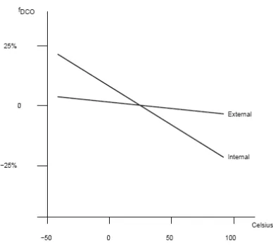
Figure 3.1: Typical DCOx range and RSELx steps vs. fDCO.
The ACLK had two main advantages over the DCO. It was very stable with ambient temperature change, and it enabled the low power mode of MSP430F2012 because we could then disable the DCO. However, the testing results showed that the 32 kHz was not high enough to execute a sample rate of 1 per second. In order to make sure our sensor system have the flexibility to change the sampling rate up to 100 per second, we chose to use the internal DCO as our primary clock source.
temperature range of 0 to 150°C. In case the frequency variation need to be further reduced, it could be software-corrected since it had an almost linear relationship with temperature change.
Figure 3.2: DCO frequency vs. temperature.
3.2.2 Sampling Rate
According to the requirement of our colleagues from food science department, the sampling rate would be between 1 to 100 samples per second. The higher the sampling rate was, the higher the DCO frequency must be. Figure 3.3 shows the relationship between active current and fDCO. To achieve 100 samples per second, the DCO frequency had to be set above 16 MHz. The required current was beyond the capacity of the BR1225A battery, which led to failure in flash memory writing.
save battery power, we used a sampling rate of 5 samples per second in most of our tests, where fDCO was around 0.8 MHz, and the battery lasted more than 16 hours.
Figure 3.3: Active mode current vs. VCC, TA, and fDCO.
3.2.3 Battery Capacity and Voltage
Table 3.7 shows the specification of our battery BR1225A [29]. Note that although the nominal voltage is 3V, but at room temperature it drops below 2.7V, as shown in Figure 3.4, which is below the threshold of flash memory chip. In our test, it was about 2.3V when battery was hooked up to the device at room temperature. As a result, we had to stack two of these batteries together to power our device to make sure of the proper behavior of the temperature sensor over its designed working range. This issue will be further discussed in next chapter, with more detailed testing results and possible alternative solution.
Table 3.7: BR1225A specification. Diameter Depth Weight Nominal
Voltage
Nominal Capacity
Continuous load
Figure 3.4: BR1225A temperature characteristics.
3.2.4 Serial On-Board Programming
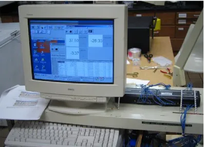
One nice feature that MSP430 series microcontrollers provided was the serial on-board programming. With the proper connections, the C-SPY debugger and an FET hardware JTAG interface, such as the MSP-FET430UIF used in our project, could be used to program and debug code on a target board. By doing this, it provided us with an easy way to re-program microcontroller, if any changes were necessary. It also was a good interface when we wanted to read the data from flash memory after any tests.
Figure 3.5 shows the connections between the 14-pin FET Interface module connector and the target device required to support in-system programming and debugging using C-SPY for 2-wire Spy-Bi-Wire communication.
V
o
lt
ag
e
(V)
Figure 3.5: Signal connections for 2-wire spy-bi-wire communication.
3.2.5 File I/O
3.2.6 Power Saving Techniques
Low power operation is a key point in this project. If we can dramatically reduce the whole power consumption, there are lots of benefits we can get. The same battery could be used for a longer time, or smaller batteries could be adopted, or the operation frequency could be increased without draining extra battery power. Low power mode (LPM) is a key feature of the MSP430 serial microcontrollers. Its design gives very low leakage, and it operates from a single supply rail. This gives an extremely low current drain when the processor is in standby mode. It could be waked up by an interrupt event such as Timer_A, which was used in our application.
Listed below are the major techniques that we had adopted in our sensor design:
a. Set the microcontroller frequency at the lowest possible level while the sampling rate can be met;
b. Let the microcontroller enter low power mode while doing analog to digital conversion;
c. Let the microcontroller enter low power mode while waiting for flash memory writing process (microcontroller being waked up by Timer_A);
d. Turn temperature sensor into standby mode when possible;
e. All unused pins are left open, switched to I/O port function, and configured as outputs, to prevent any unnecessary power consumption; and
packaging and experiment setup (in this case, the power saving is not only from microcontroller, but, more importantly, from letting the flash memory into standby mode).
3.3 Sensor Design - Hardware
3.3.1 System Schematic and PCB Design
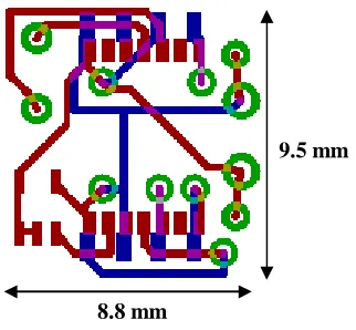
A system schematic of our off-the-shelf temperature sensor is shown in Figure 3.6. Two BR1225A batteries were used as power source in the sensor system. A decoupling capacitor was necessary in this project. Without that, the current provided by batteries themselves was not enough when data were written to the flash memory. The microcontroller converted the analog voltage signals from the temperature sensor into digital numbers. After that, data were stored in the Atmel flash memory in binary format. A two-sided printed circuit board (PCB) was designed with EAGLE. The layout was shown in Figure 3.7. The size of the board was smaller than 10 mm by 9 mm. If we use surface-mount decoupling cap and power switch, the overall dimension can be shrunk down to 8 mm by 7 mm.
Figure 3.6: System schematic of our temperature sensor. NS
LM94 TI MSP430
Figure 3.7: PCB layout of our temperature sensor.
Our off-the-shelf temperature sensor is shown in Figure 3.8. The overall dimension was 12.5 x 12.5 x 9 (mm) with two batteries, or 12 x 12 x 4 (mm) without any battery.
Figure 3.8: Off-the-shelf temperature sensor (left top: front view w/o battery; left bottom: front view with batteries; right top: back view; right bottom: horizontal view with two
batteries).
9.5 mm
3.3.2 On-Board Programming Setup
The on-board programming setup is shown in Figure 3.9. On the left side of the picture was the MSP-FET430UIF which connected the setup to the USB port on a desktop PC. This setup was used for debugging, re-programming, and data reading.
Figure 3.9: On-board programming setup.
3.4 Sensor Design - Software
3.4.1 Microcontroller Programming - Write
Microcontroller had been successfully programmed in C using IAR Embedded Workbench, which is a very powerful Integrated Development Environment, which allows users to develop and manage complete embedded application projects.
By specifying the appropriate opcode and then following the required steps, users can either write data to it or read data from it. To initiate a write operation, an 8-bit opcode of 82H must be followed by the four reserved bits and 20 address bits. After all address bits were shifted in, the part took data from the SI pin and stored it in one of the data buffers. When there was a low-to-high transition on the CS pin, the data stored in the buffer was transferred into the specified page in the main memory. Following is the pseudo code:
void main(void) {
Stop Watch-Dog Timer(WDT); Setup DCO frequency;
Enable and setup 10-bit ADC; Packaging_standby ();
Setup I/O directions;
for (Page = 0; Page < 2048; Page ++) {
for (Byte = 0; Byte < 264; Byte = Byte + 2) { Start ADC;
Shift in opcode (82H) and 20 address bits; Store 10-bit ADC result in flash memory; All inputs finished, set CS to be high; Data_transfer_standby(); } }
3.4.2 Microcontroller Programming - Read
After the test, we had to pull data out from the flash memory, so another program was designed to do this job. To start a read operation, an opcode of 52H must be clocked into the flash memory chip, followed by 24 address bits and 32 don’t care bits. After that, additional pulses on SCK resulted in serial data being output on the SO (serial output) pin. A low-to-high transition on the CS pin terminated the read operation and tri-state the SO pin. All data was saved in a text file named “TermIO.log”. It took a few hours to output all data from memory chip. Following is the pseudo code:
void main(void) {
Stop Watch-Dog Timer(WDT); Setup Max DCO frequency; Setup I/O directions;
for (Page = 0; Page < 2048; Page ++) {
for (Byte = 0; Byte < 264; Byte = Byte + 2) {
Shift in opcode (52H), 20 address bits, and 32 don't care bits; Read the 10-bit ADC result stored in flash memory;
Convert binary number to decimal; Printf();
3.4.2 C Programming - Conversion
After we got the file “TermIO.log”, we used another regular C code to convert decimal numbers into real temperatures. The results were saved in a text file named “temperature_log.txt”. Following is the pseudo code:
void main(void) {
char record[100], *fld; FILE * fin; FILE * pFile;
fin = fopen("TermIO.log", "r"); pFile = fopen ("temperature_log.txt","w");
while (fgets(record, sizeof(record), fin) != NULL) { fld = strtok(record, " \n\0\r\t");
Decimal = atoi(fld);
Voltage = decimal2voltage (Decimal);
Temperature = voltage2temperature (Voltage); fprintf (pFile,"%f ",Temperature);
fprintf (pFile,"\n"); }
CHAPTER 4
Off-the-shelf Sensor Testing and
Verification
Off-the-shelf temperature sensor was successfully developed as described in last chapter. In this chapter, we mainly focus on the sensor testing and verification. After device packaging and the experiment setup is introduced, we show some primary measurement results in validation phase I in section 4.2. In section 4.3, we present the validation study phase II which determines the accuracy of temperature measurement. At the end of this chapter are the discussion and proposal for future work.
4.1 Device Packaging and Experiment Setup
Figure 4.1: Prepare the polypropylene hemispheres.
Figure 4.3: Experiment setup for the batch validation studies.
4.2 Validation Phase I
4.2.1 Physical Measurements
The sensor particle had to be neutrally buoyant with water so that it would not sink during the aseptic processing. Therefore, physical parameters were first measured in order to calculate the density of the particle. We found out that, although the sensor could fit in the ¾” sphere package, the density (1.21 g/cm3
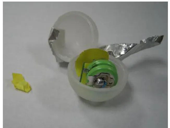
to make it work. For example, to obtain neutral buoyancy at 100°C, approximately 2 gram should be added inside the sphere. Magnets or small RFID tags could be added for the purpose of position tracing. A sensor in 1” sphere package is shown in Figure 4.4. There was still lot of space left. The yellow item next to the sensor was a piece of magnet used to balance the weight.
Table 4.1: Density calculation of off-the-shelf sensor packages. Size (mm) Volume (cm3) Weight (g) Density
(g/cm3) Sensor before
Packaging
12.5 x 12.5 x
9 - 2.93 g -
Sensor in ¾”
Sphere - 3.619 4.47 g 1.21
Sensor in 1”
Sphere - 8.58 6.15 g 0.716
4.2.3 Battery Duration
Battery duration was also measured in tests. Results showed that at high sampling rate (50 samples per second) the two batteries could last more than 4 hours. At normal sampling rate (5 samples per second) the batteries lasted more than 16 hours. Beyond that time, microcontroller and temperature sensor were still working properly, but error began to occur in flash memory writing.
4.2.4 Temperature Measurement Range
Range of temperature measurement was roughly determined to be 10-140°C. The highest temperature our sensors had ever recorded was about 140°C. Although we had not tried 150°C, majorly due to lab safety concerns, we believe there are good chances that this sensor could work at 150°C.
The sensor failed to work when ambient temperature went down to 10°C. If we recall Figure 3.4 in Chapter 3, the voltage of battery drops with temperature. When temperature was below 10°C, battery voltage, which was the total voltage of 2 batteries in series, dropped below the threshold of flash memory chip. Again, microcontroller and temperature sensor were still working properly, but it could not write any data to flash memory.
4.2.5 ADC Error Estimation
results in Table 4.2 showed that the ADC error was less than 3%. However, if we need more precise ADC results, we can use MSP430F2013 microcontroller which has a 16-bit sigma-delta ADC, at the cost of higher power consumption.
Table 4.2: ADC test results.
Input voltage 5.00 4.06 3.86 3.30 2.27 1.91 0.79 0.16 0.00 ADC Results 1023 840 784 670 472 395 170 34 0
4.3 Validation Phase II (Batch Validation)
In validation study phase II, our main goal was to determine the accuracy of temperature measurement. Since continuous flow test was not available, we only focused on batch test (zero relative velocity between the fluid and particle).
4.3.1 Mild Temperature Tests
Mild Temp Test
0 10 20 30 40 50 60 70 80
0 500 1000 1500 2000 2500
Second
° C
Figure 4.5: A mild temperature test (blue: temperature recorded by data acquisition device; pink: temperature points recorded in flash memory).
4.3.2 Temperature Recording Noise
Although in Figure 4.5 it showed smooth temperature transition, there were small up and down variations by looking into each page. Even though the overall plot showed the temperature rising as expected, these small variations up and down variations in temperature, as shown in Figure 4.6, were of our concern. Since ambient temperature was always higher that the temperature of sensor, we would expect a consistent rise without the small retreats.
pink dots in Figure 4.6 were the temperature data after taking average of every 5 samples. Result demonstrated that this method had effectively eliminated the small up and down variations in the temperature record.
60 61 62 63 64 65 66 67
0 10 20 30 40 50
°C
60 61 62 63 64 65 66 67
0 10 20 30 40 50
°C
Figure 4.6: Temperature variations (left: original data; right: data after averaging).
One drawback of this method is that it decreases the sampling rate. Other techniques to suppress the variation include oversampling, median filtering, better PCB design, decent power plan, larger decoupling cap, etc.
4.3.3 High Temperature Tests
actually was. That was why the blue curve changed sometime before the pink one does, and also why the peak of temperatures recorded in flash memory was lower than the peak of the blue curve.
Figure 4.7: High temperature test results (blue: temperature recorded by data acquisition device; pink: temperature points recorded in flash memory).
Since the thermocouple was not fixed in the package, it had chance to move inside of the sphere. When it touched the batteries, wires, or came close to the inner surface of the sphere, abnormal reading occurred, just like what happened in Figure 4.7 when temperature was dropping. There were also variations in the temperature recording, as shown in Figure 4.8. Those variations were eliminated by median filtering. Results are shown in Figure 4.9.
High Temp Test - 1
0 20 40 60 80 100 120 140
0 500 1000 1500
Second
High Temp Test - 1 75 80 85 90 95 100 105
600 650 700 750 800
Second
°C
High Temp Test - 1
75 80 85 90 95 100 105
600 650 700 750 800
Second
°C
Figure 4.8: Temperature variations (left: original data; right: data after filtering).
High Temp Test - 1
0 20 40 60 80 100 120 140
0 500 1000 1500
Second
° C
Figure 4.9: Temperature reading after filtering.
High Temp Test - 2
0 20 40 60 80 100 120 140
0 500 1000 1500
Second
° C
Figure 4.10: High temperature test results (blue: temperature recorded by data acquisition device; pink: temperature points recorded in flash memory).
We had also processed the data with median filtering technique. Results are shown in Figure 4.11. Since the two curves almost overlapped at their peaks, it gave us a good opportunity to estimate the accuracy of our temperature sensor. From Figure 4.12, we found out that the difference between them was less than 1°C. Taking into account that thermocouple reading should be slight higher, the actual difference was even smaller.
High Temp Test - 2
0 20 40 60 80 100 120 140
0 200 400 600 800 1000 1200 1400
Second
° C
Figure 4.11: Temperature reading after filtering.
High Temp Test - 2
115 115.5 116 116.5 117 117.5 118 118.5 119 119.5 120
800 850 900 950 1000 1050
Second
°C
4.1 Discussion and Proposed Improvement
4.1.1 Temperature Variations
Low sampling rate would help reduce the variations in temperature recording. Figure 4.13 shows the results from one of our tests with sampling rate at one per second. Although there were still small variations, it was clearly much smoother than what we obtained from tests at high sampling rate. Using larger capacitor also helps, and we should try to let batteries and capacitor stay as close to the device as them could.
Test
20 30 40 50 60 70 80 90 100 110
0 200 400 600 800 1000 1200 1400
Second
° C
Figure 4.13: Temperature test at low sampling rate.
4.1.2 Temperature Sensor Calibration
well-controlled furnace and a precise thermal sensor, we can re-calibrate our temperature sensor and improve its overall performance.
4.1.3 Other Components
There are some other components we might want to consider, as listed in Table 4.3. The reasons that they were not used in our project in the first place are also specified below. Originally we wanted to limit our sensor size to be 8mm by 8mm by 8mm. Since we had switched to a 1” sphere package later due to the density requirement, lots of them might be reconsidered for our project.
Table 4.3: Other possible components.
Memory Battery Microcontroller Sensor
Device
Atmel Flash Memory 2.5V
version
BR1623A MSP430F2013 MAX6641
Features
Lower threshold voltage requirement
120 mAh, higher nominal voltage
16-bit
sigma-delta ADC +/-1°C Accuracy
Reasons N/A on market Size Power Size (3 mm x 5
mm x 0.9 mm) Comments Can increase sensor working range 16mm diameter; 1.5 gram
Have to change codes
CHAPTER 5
CMOS Sensor Design
While off-the-shelf sensors being developed and tested, integrated CMOS temperature sensor was also investigated. Thanks to the advanced IC processing technology, CMOS sensors are able to provide low-cost and high-performance solutions in the area of temperature sensing [30-31]. There are various kinds of CMOS temperature sensors being used in many fields in the industry as well as in household equipment [32-33]. Typical applications include: 1) the environment temperature monitor, used in automatic manufacturing factories; 2) the temperature control of consumer electronics, such as automobiles and home electronics; and 3) the power consumption control in VLSI chips, such as CPU and chip sets; and 4) the thermal compensation in single-chip systems and micro systems with built-in sensors.
sensors because of lower cost and better compatibility. Recently there has been a growing interest in designing a new family of CMOS sensors, called smart sensors or integrated sensors, which refers to the sensors with on-board analog to digital converters [37-40]. Because of the digital interface requirement, CMOS sensors are therefore more favorable. Compared to off-the-shelf temperature sensors, the CMOS sensors have the advantages of smaller area (less than 1 mm2) and lower power consumption (less than 1 mW). Also it is possible to be incorporated in other techniques such as RFID. It is able to provide precise measurements with an accuracy of 1°C or less after a two point calibration, without any complicated curvature correction. The disadvantages of CMOS sensors include high development cost and poor expansibility.
In this chapter, we first review the different types of CMOS temperature sensors in section 5.1. In section 5.2, we present our CMOS sensor design with simulation results.
5.1 CMOS Sensor Overview
analog output signals i.e. current-output signals or voltage-output signal. In order to interface between the analog sensor and the digital environment, ADC (analog to digital converter) has been developed to output digital signals. Because of its reliable performance in most low-frequency applications, more than half of CMOS sensors are using sigma-delta A/D converters [38]. However, despite of its excellent performance, sigma-delta A/D converters have complex structures and are not area-efficient. Therefore, many digital temperature sensors have been designed with different ADC schemes. Several research groups are dealing with the design of ring-oscillator-based temperature sensors. For example, a temperature-dependent resistor can be use to control the charging/discharging current of the oscillator stages [42]. In this way, the temperature data is converted to a shift in the oscillation frequency. Another example is a time-digital-converter-based temperature sensor [39]. It is proposed for low-cost, low-power and high-accuracy on-chip integrations. One of its delay lines consists of multiple temperature compensated delay cells to reduce the thermal sensitivity. In contrast, another delay line is composed of an even number of NOT gates (or multiple equivalent delay buffers) without thermal compensation. A counter is used to count the circulation times of the input interval and generates the corresponding digital output.
5.2 CMOS Temperature Sensor Design
5.2.1 Design Overview
unit. The output signal of the current to frequency converter was a square-wave which carried the temperature information from the sensor. This frequency was then turned into a digital number by counting the square-wave pulses in the digital control unit, and it stored the information in the flash memory.
Figure 5.1: Scheme of CMOS temperature sensor design.
5.2.2 Temperature Sensor and Frequency Converter
The schematic of temperature sensor and frequency converter is shown in Figure 5.2. It was originally designed by Vladimir Szekely with the Technical University of Budapest, Hungary [43]. The first part of this circuit was a temperature with current output, and the second part was a current to frequency converter which generated square-wave carrying the temperature information. The p-channel transistor M1, M2, M3, and M4 constituted a cascade current mirror, which mirrored the current of M6 to transistor M5 and M7. Being in another current mirror, the current in M8 and M11 followed the current in M5 and M7. The main advantage of this circuit was the stable operation. The output current and the VC and VD voltages were
Temp Sensor Oscillator
Internal Clock
practically independent of the supply voltage. The voltages at nodes C and D could be expressed as
(1 ) 65 67 12 12 X X X X V
VC T
− − +
= (1)
(1 ) 65 67 12 67 X X X X V
VD T
− − +
= (2)
where Xpq was the size ratio of transistor p and transistor q.
Figure 5.2: Schematic of temperature sensor and frequency converter.
The current output of the sensing circuit IM8 was controlled by voltage VD, which was temperature dependent. Thus it led us to the following expression:
2 2 65 67 12 67 2 11
8 M T ( ) T
M CV X X X X V I = − −
=β (3)
T dT dV V dT d I
IM T
∆ + =
∆ 8 1 β 2
β (1)
M1 M2 M10
M3 M4 M9
M5 M8
M6 M7 M11
Di ff ere n tial C om p a r at or N M T
A T
N M
N M
C
D C
D
where C was a constant, and VT and β were for n-channel transistors.
The current to frequency converter was built using a simple differential comparator. The output current of the analog sensor IM8 and the current generated by a current mirror IM9 charged and discharged the capacitor C3. The signal of the capacitor was one of the inputs to a differential comparator. The reference voltage of the comparator was switched by voltages VC and VD. By comparing those two signals, the differential comparator outputted a square wave. The waveforms of the comparator are shown in Figure 5.3.
Figure 5.3: Waveforms of differential comparator.
The output of the differential comparator was sent to a series of inverters, resulted the final frequency of:
) (
2 3
8
D C M
V V C
I f
− ⋅
Because the current output IM8, VC and VD voltages were all independent of the supply voltage, the resulting frequency was also independent of the supply voltage.
5.2.3 Internal Clock
Current starved ring oscillator is a good candidate as internal clock generator in low power systems. In our project, the independence of the clock to both of the supply voltage and temperature was required to store temperature information at a stable rate in the flash memory. The schematic of a temperature compensated ring oscillator is shown in Figure 5.4. It is originally designed by Namjun Cho with the Korea Advanced Institute of Science and Technology [44].
Figure 5.4: Schematic of internal clock.
CTAT
1 2 3 4
IB
PTAT
5 6 7 8
IA 9
13
I
refA CTAT (complementary to absolute temperature) circuit was on the left side, generating a bias current IB which was decreasing with temperature rising. Next to the CTAT is a PTAT (proportional to absolute temperature) circuit with a current IA increasing with temperature. The current IB was mirrored by transistor pair M2 and M13, and then mirrored by transistor pair M10 and M11. The current IA was mirrored by transistor pair M9 and M12. By carefully matching the magnitude of these two currents, the bias current Iref, which was the sum of those two, became independent of temperature and was supplied to the current starved ring oscillator. In order to suppress the sensitivity of output frequency to supply voltage changes, cascade current mirrors were used, which was constituted of transistor M1, M2, M3, and M4 in the CTAT circuit and of transistor M5, M6, M7, and M8 in the PTAT circuit. Thus the clock circuit generated an output frequency that was independent of both supply voltage and ambient temperature.
The frequency of the internal clock was set to be 2 MHz. At this frequency, the sampling rate could go as high as 1000 times per second. In case we don’t need such high rate, the clock frequency can be reduced to save power.
5.2.3 Digital Control Unit Design
Figure 5.5: Block diagram of digital control unit.
This ASIC consisted of four main parts, pre-counter, counter, selectable delay line, and address generator. When the circuit started to work, the “pre-counter” determined when the counter should begin (it began at the next rising edge of the sensor signal). The “counter” was the block where 12-bit ADC was done. When “counter” received the “count start” signal, it began counting at every rising edge of the clock for 255 cycles of the temperature sensor’s output. At the 256th
rising edge of the sensor signal, the ADC was finished and thus the frequency signal was converted to a 12-bit digital result.
It first generated the appropriate page and byte addresses, and then clocked the ADC results into the flash memory through three pins, CS, SI and SCK. When it finished, it sent out a “start over” signal and a new round began until the end of the memory was reached.
5.2.4 Simulation Results
A. Performance
The clock circuit generated a clock signal at 2 MHz. It was very stable over temperature variations, with sensitivity less than 0.02 %/°C. The simulated frequency output of the temperature sensor versus ambient temperature is shown in Figure 5.6. The frequency varied from 0.98 MHz to 0.21 MHz at the temperature range of 0°C to 150°C. The slope was about -0.97 %/°C.
Frequency VS Temperature
0 0.1 0.2 0.3 0.4 0.5 0.6 0.7 0.8 0.9 1
0 50 100 150 200
Temperature (°C)
F re qu e n c y ( M H z)
Figure 5.7 shows the waveforms of the ASIC circuit over first a few sample cycles, and Figure 5.8 focuses on the output waveforms of the address generator. When the ADC was done and “count finish” signal was on, the address generator started to work by sending out opcode 82H, followed by 11-bit page address and 9-bit byte address. Then the 12-bit ADC result had been clocked out. After that it set “start over” signal high and new A/D conversion began. The sampling speed could change from 1 to 1000 samples per second, selectable by end users. The ADC accuracy was less than 0.1°C.
Figure 5.7: ASIC circuit waveforms.
B. Layout and Size
The layout of both of the clock and the temperature sensor was completed in IBM 7RFML 180nm process. The layout is shown in Figure 5.9, with a total area of 0.0085 mm2.
Figure 5.9: Layout of the clock and the temperature sensor.
The ASIC was synthesized in Synopsys, and then placed and routed in Encounter with iit018 standard cell library. The final layout is shown in Figure 5.10, with a total area of 0.045 mm2.
C. Power
Without that, the clock was able to run at extremely low current. The evaluation of the power consumption of the ASIC was little more complicated. It involved the determination of the switching activity associated with the nets in the design, so it had to be done after routing, with a test fixture of its typical activities. Simulation in design complier showed that the whole power consumption was 0.284 mW, with 0.193 mW on clock.
D. Summary
Table 5.1 contains the summary of our CMOS sensor, over a temperature range from 0°C to 150°C. The CMOS sensor had a total area of 0.054 mm2
, an averaged power consumption of 0.8 mW, and an accuracy of less than 0.2°C.
Table 5.1: Technical summary of CMOS sensor.
Size (mm2) Power (mW) Output (Hz) Sensitivity Temp Sensor 0.015 - 0.019 0.21M – 0.89M Δf/(f*ΔT) = 0.97 %
Clock 0.0085 0.47 - 0.51 2.0M Δf/(f*ΔT) < 0.02 %
Digital Unit 0.045 0.284 1 - 1000 ADC Accuracy < 0.1°C
Total 0.054 0.76 – 0.91 - Accuracy < 0.2°C
CHAPTER 6
Conclusion and Future Work
5.1 Conclusion
Food safety is rapidly becoming one of the most critically important issues in food industry. With the increasing consumer demand for convenient, high quality, and healthy foods, aseptic processing was proposed as a potential option to meet these demands. In order to validate such a system and also make the process relatively inexpensive, researchers have to find out the “critical particle” in the processing system and determine its time-temperature history.
While the off-the-shelf sensors being designed and tested, integrated CMOS temperature sensor had also been investigated. Compared to off-the-shelf temperature sensors, the CMOS sensors have the advantages of smaller area and lower power consumption. The CMOS sensor design and simulation results have been presented in details in Chapter 5. It had a total area of 0.054 mm2, an averaged power consumption of 0.8 mW, and an accuracy of less than 0.2°C.
The significance of this study lies in the development of a validated tool and technique that can be used to facilitate validating aseptic processing of multiphase foods and thereby provide the health-conscious consumer with a high quality food product. The results of our project can be useful to food processors for conducting validation studies as part of the process filing procedure for multiphase food products. Our sensors and testing methodology can be used to demonstrate to the FDA or USDA that the simulated particle will have conservative heating and flow characteristics which will ensure the adequacy of the process and the safety of the food product.
hitherto unavailable due to their potentially low quality (due to the inherent over-processing in a typical retort canning process).
5.2 Future Work
Apart from the work that has been done with respect to the development of temperature sensors for food processing, the future work will involve additional testing and validation, device miniaturization and optimization, and design of CMOS sensor with on-board memory and RF telemetry.
5.2.1 Off-the-shelf Sensor
Modification is needed to help reduce the noise in temperature recording. With a well-controlled furnace and a precise thermal sensor, the off-the-shelf sensor can be re-calibrated and its overall performance will be improved. More batch tests need to be done, and continuous flow tests also need to be started to ensure that the sensor system would conservatively determine the temperature within the particle at any intermediate processing condition, over the widest possible range of parameters.
5.2.2 CMOS Sensor and RFID
CMOS temperature sensor has been design in this thesis. However it is just a prototype without on-board memory and RF telemetry, which are desired for our project. Further research has to be done to incorporate these elements in the CMOS sensor. Other techniques including on chip antenna, battery-less operation and position tracking system may also be investigated for this project.
As being discussed before, accurate determination of the time-temperature history at critical point in a system will greatly simplify the validation process for any aseptic food processing. The use of RFID (Radio Frequency Identification) combined with our temperature sensor is a promising technique to solve this problem [45-46].