ISSN(Online): 2320-9801
ISSN (Print): 2320-9798
I
nternational
J
ournal of
I
nnovative
R
esearch in
C
omputer
and
C
ommunication
E
ngineering
(An ISO 3297: 2007 Certified Organization) Website: www.ijircce.com
Vol. 5, Issue 3, March 2017
Design of DADDA Multiplier with CSC and
Low Power Scan Based Test Using DFT
S.Magdalin1, J.R.Dinesh Kumar2,
PG Student, Dept. of ECE, Karpaga Vinayaga College of Engineering and Technology, Chennai, India
Assistant Professor, Dept. of ECE, Karpaga Vinayaga College of Engineering and Technology, Chennai, India
ABSTRACT: A new low-power (LP) scan-based built-in self-test (BIST) technique is proposed based on weighted pseudo-random test pattern generation and reseeding. A new LP scan architecture is proposed, which supports both pseudorandom testing and deterministic BIST. Precise models and algorithms are not always suitable for efficient for use in the applications. Multiplication using DADDA multipliers has higher speed compared to conventional multipliers are also using approximate prediction technique for carry. They are quite effective for carry. This effective in terms of power dissipation, when high speed is required. In both the cases, only a small number of scan chains are activated in a single cycle. Sufficient experimental results are presented to demonstrate the performance of the proposed LP BIST approach.
KEYWORDS: Low-power (LP) built-in self-test (BIST), reseeding, scan-based BIST, DADDA Multiplier. Speculative Compressor.
I. INTRODUCTION
The power and ever-increasing test power. Problems, such as excessive heat that may reduce circuit reliability, formation of hot spots, difficulty in performance verification, reduction of the product yield and lifetime, and so on, have become severe [15] [16]. More details on how to provide more accurate power model can be found from [15] and [16]. fast simulation approach was proposed for low-power (LP) off-chip interconnect design in[8]. An important through silicon via (TSV) modeling/simulation technique for LP 3-D stacked IC design was presented in [62]. Furthermore, the power dissipation of scan-based built-in self-test (BIST) is much higher than power dissipation in patterns. Therefore, it is essential to propose an effective LP BIST approach.
Recent methods in aim at reducing the switching activity during scan shift cycles, whose test generator allows automatic selection of their parameters for LP pseudorandom test generation. However, many of the previous LP BIST approaches cause fault coverage loss to some extent. Therefore, achieving high fault coverage in an LP BIST scheme is also very important. deterministic scan testing due to excessive switching activities caused by random.
In this paper, we propose a new LP scan-based BIST architecture, which supports LP pseudorandom testing, LP deterministic BIST and LP reseeding. We present the major contributions of this paper in the following.
1) A new LP weighted pseudorandom test pattern generator using weighted test-enable signals is proposed using a new clock disabling scheme. The design-for-testability (DFT) architecture to implement the LP BIST scheme is presented. Our method generates a series of degraded sub circuits. The new LP BIST scheme selects weights for the test-enable signals of all scan chains in each of the degraded sub circuits, which are activated to maximize the testability.
ISSN(Online): 2320-9801
ISSN (Print): 2320-9798
I
nternational
J
ournal of
I
nnovative
R
esearch in
C
omputer
and
C
ommunication
E
ngineering
(An ISO 3297: 2007 Certified Organization) Website: www.ijircce.com
Vol. 5, Issue 3, March 2017
3) Testing all the memories in these SoCs serially would take a long time. Therefore, a memory BIST design that allows two or more memories to be tested simultaneously is needed. So in case when the memories are tested in parallel (concurrently) the consumed power is the sum of the powers consumed by each memory. Hence, parallel run of memories by the same BIST scheme will consume much power.
which means that there could be a limitation on sharing multiple memories by the same BIST scheme. Total test application time of a memory BIST is also calculated under maximum power constraint [2]. Consequently, power consumption is one of the most critical constraints for SoCs. Moreover, the increasing functionality also raises complexity for specification, design and verification of SoCs. Therefore, power aware design should be introduced at early stages of SoC design where it has the highest benefits for power reduction [3].
II. RELATED WORK
Scan flip flops, especially, the ones close to the scan-in pins, are not observable in most of shift cycles. Proposed a novel BIST scheme that inserts multiple capture cycles after scan shift cycles during a test cycle. Thus, the fault coverage of the scan-based BIST can be greatly improved. An improved method of the earlier work, presented in, selects different numbers of capture cycles after the shift cycles. In this paper, a new LP scan-based BIST technique is proposed based on weighted pseudorandom test pattern generation and reseeding. A new LP scan architecture is proposed, which supports both pseudorandom testing and deterministic BIST.
Weighted pseudorandom testing schemes can effectively improve fault coverage. A weighted test-enable signal-based pseudorandom test pat-tern generation scheme was proposed for scan-signal-based BIST, according to which the number of shift cycles and the number of capture cycles in a single test cycle are not fixed. A reconfigurable scan architecture was used for the deterministic BIST scheme in using the weighted test-enable signal-based pseudorandom test generation scheme. A low-transition test pattern generator was proposed to reduce the average and peak power of a circuit during test by reducing the transitions among patterns. Transitions are reduced in two dimensions:
1) Between consecutive patterns. 2) Between consecutive bits.
LP BIST technology that reduces shift power by eliminating the specified high-frequency parts of vectors and also reduces capture power. The approach to reduce peak power and power droop during capture cycles in scan-based logic BIST. An efficient BIST architecture was recently presented for targeting defects in dies and in the interposer interconnects. low-power BIST technology was proposed that reduces shift power by eliminating the specified high-frequency parts of vectors and also reduces capture power. Multi cycle tests support test compaction by allowing each test to detect more target faults. The ability of multi cycle broadside tests to provide test compaction depends on the ability of primary input sequences to take the circuit between pairs of states that are useful for detecting target faults. This ability can be enhanced by adding DFT logic that allows states to be complemented. Complete fault coverage can be obtained when the pseudorandom test generator is modified. A combination of a pseudorandom test generator and a combinational map-ping logic was constructed produce a given target pattern set of the hard-to-detect faults. which encoded deterministic vectors into seeds.
ISSN(Online): 2320-9801
ISSN (Print): 2320-9798
I
nternational
J
ournal of
I
nnovative
R
esearch in
C
omputer
and
C
ommunication
E
ngineering
(An ISO 3297: 2007 Certified Organization) Website: www.ijircce.com
Vol. 5, Issue 3, March 2017
BIST 2 BIST 3
BIST 1
Memory1 Memory2 Memory3 Memory4
Figure 1. Memory BIST architecture.
III. CIRCUIT DESIGN
In Fig. 2, the proposed BIST circuit is depicted. It consists of a nMOS transistor pair DUT1,n and a pMOS pair DUT1,p, respectively. The gates of the two transistors of a selected pair are operated with complementary clock signals, the gates of the non-selected pair are deactivated. The pairs are operated as current sinks [10], so that in case of the pMOS pair the S/D terminals represent the input of the sink, whereas in case of the nMOS pair the well takes over this role. All other terminals are connected to voltage Vmid, which is typically in the range of VDD /2. The current sink’s input is held at the same voltage through the regulation loop consisting of OP1 and M1. The charge pumping current is integrated on capacitor Cint (100 pF) which is pre-charged to 0 V at the beginning of a measurement cycle. The master clock used to generate the gate voltages of the DUTs also drives a counter which is stopped by comparator COMP1 once a voltage (VDD-Vref) is integrated on Cint. For each clock cycle, the selected DUT draws a charge packet Dit × Wtotal × L × q from Cint, so that the counter stop condition is fulfilled for
N – 1 < Cint (VDD – Vref) / (Dit × Wtotal × L × q)d N (2)
with N being the number of counted pulses. An SPI interface is used to continuously stream out the measured value N. Moreover, it controls the DUT operating conditions using a small state machine. The interface can communicate thousands of A/D measurement values from the BIST structure during a few milliseconds to an external control unit e.g. during a ramp-up period of an ASIC or a SoC for a given application.
Figure 2.Circuit diagram of the core BIST structure.
ISSN(Online): 2320-9801
ISSN (Print): 2320-9798
I
nternational
J
ournal of
I
nnovative
R
esearch in
C
omputer
and
C
ommunication
E
ngineering
(An ISO 3297: 2007 Certified Organization) Website: www.ijircce.com
Vol. 5, Issue 3, March 2017
IV. THE PROPOSED DESIGN
Design for testing or design for testability (DFT) consists of IC Design techniques that add testability features to a hardware product design. The added features make it easier to develop and apply manufacturing tests to the designed hardware. The purpose of manufacturing tests is to validate that the product hardware contains no manufacturing defects that could adversely affect the product’s correct functioning. Tests are applied at several steps in the hardware manufacturing flow and, for certain products, may also be used for hardware maintenance in the customer’s environment. The common understanding of DFT in the context of Electronic Design Automation (EDA) for modern microelectronics is shaped to a large extent by the capabilities of commercial DFT software tools as well as by the expertise and experience of a professional community of DFT engineers researching, developing, and using such tools. Much of the related body of DFT knowledge focuses on digital circuits while DFT for analog/mixed-signal circuits takes somewhat of a backseat.
To simplify test generation, DFT addresses the accessibility problem by removing the need for complicated state transition sequences when trying to control and/or observe what’s happening at some internal circuit element. Depending on the DFT choices made during circuit design/implementation, the generation of Structural tests for complex logic circuits can be more or less automated. Approximate circuits have been considered for error-tolerant applications that can tolerate some loss of accuracy with improved performance and energy efficiency. Multipliers are key arithmetic circuits in many such applications such as digital signal processing (DSP). In this paper, a novel approximate multiplier with a lower power consumption and a shorter critical path than traditional multipliers is proposed for high-performance DSP applications.
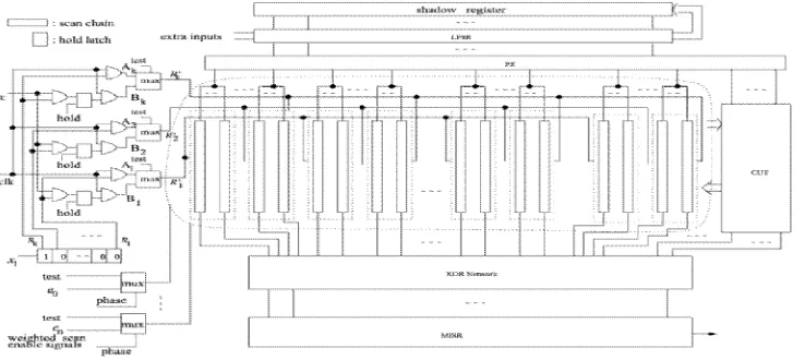
Figure 3.General DFT architecture for LP scan-based BIST.
ISSN(Online): 2320-9801
ISSN (Print): 2320-9798
I
nternational
J
ournal of
I
nnovative
R
esearch in
C
omputer
and
C
ommunication
E
ngineering
(An ISO 3297: 2007 Certified Organization) Website: www.ijircce.com
Vol. 5, Issue 3, March 2017
Figure 4.architecture of approximate multiplier.
V.RESULTS
Given the complete approach presented above, one can easily observe that the number of test clusters depends linearly on a deterministic pattern count targeting random-resistant faults. Moreover, the children pattern count for each test cluster initially matches the size of the longest scan chain (or the number of scan shift cycles). Needless to say, a random pattern resistant fault list may easily contain millions of faults. The implications of these facts become apparent as we begin to consider relevant memory and CPU time requirements. Clearly, with the increasing size of designs, the presented flow may turn out to be less practical as the memory footprint and time needed to complete the ordering process can be prohibitive for large circuits. Consequently, to alleviate these problems, we propose below a more pragmatic and scalable solution.
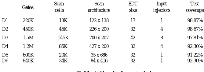
Gates Scan Scan EDT Input Test
cells architecture size injectors coverage
D1 220K 13K 122 x 138 17 1 98.87%
D2 450K 45K 226 x 200 32 4 98.67%
D3 1.5M 145K 700 x 207 42 8 97.81%
D4 1.2M 85K 427 x 200 32 4 92.30%
D5 600K 20K 35 x 686 32 1 91.22%
D6 840K 34K 84 x 416 32 1 92.30%
Table 1 Circuit characteristics.
ISSN(Online): 2320-9801
ISSN (Print): 2320-9798
I
nternational
J
ournal of
I
nnovative
R
esearch in
C
omputer
and
C
ommunication
E
ngineering
(An ISO 3297: 2007 Certified Organization) Website: www.ijircce.com
Vol. 5, Issue 3, March 2017
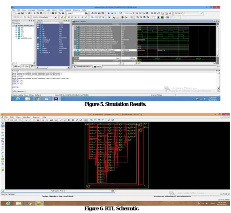
Figure 5. Simulation Results.
Figure 6. RTL Schematic.
ISSN(Online): 2320-9801
ISSN (Print): 2320-9798
I
nternational
J
ournal of
I
nnovative
R
esearch in
C
omputer
and
C
ommunication
E
ngineering
(An ISO 3297: 2007 Certified Organization) Website: www.ijircce.com
Vol. 5, Issue 3, March 2017
Figure 7. Tabulated parameter for area.
Figure 8. Tabulated parameter for power.
Figure 9. Tabulated parameter of delay.
VI.CONCLUSION
ISSN(Online): 2320-9801
ISSN (Print): 2320-9798
I
nternational
J
ournal of
I
nnovative
R
esearch in
C
omputer
and
C
ommunication
E
ngineering
(An ISO 3297: 2007 Certified Organization) Website: www.ijircce.com
Vol. 5, Issue 3, March 2017
Xilinx ISE design suite 14.5. The performance of the approximate multiplier can further be improved by considering don’t care conditions and further by using variable latency adder.
REFERENCES
[1] A. S. Abu-Issa and S. F. Quigley, “Bit-swapping LFSR and scan-chain ordering: A novel technique for peak- and average-power reduction in scan-based BIST,” IEEE Trans. Comput.-Aided Des. Integr. CircuitsSyst., vol. 28, no. 5, pp. 755–759, May 2009.
[2] V. D. Agrawal, C. R. Kime, and K. K. Saluja, “A tutorial on built-in self-test. I. Principles,” IEEE Des. Test Comput., vol. 10, no. 1, pp. 73–82, Mar. 1993.
[3] A. Al-Yamani, N. Devta-Prasanna, E. Chmelar, M. Grinchuk, and A. Gunda, “Scan test cost and power reduction through systematic scan reconfiguration,” IEEE Trans. Comput.-Aided Des. Integr. Circuits Syst., vol. 26, no. 5, pp. 907–918, May 2007.
[4] Synopsys. ASTRO: Advanced Place-and-Route Solution forSoC Design, accessed on Mar. 1, 2015.
[5] M. Nourani, M. Tehranipoor, and N. Ahmed, “Low-transition test pattern generation for BIST-based applications,” IEEE Trans. Comput., vol. 57, no. 3, pp. 303–315, Mar. 2008
[6] S. Banerjee, D. R. Chowdhury, and B. B. Bhattacharya, “An efficient scan tree design for compact test pattern set,” IEEE Trans. Comput.-Aided Des. Integr. Circuits Syst., vol. 26, no. 7, pp. 1331–1339, Jul. 2007.
[7] P. H. Bardell, W. H. McAnney, and J. Savir, Built in Test for VLSI:Pseudorandom Techniques. New York, NY, USA: Wiley, 1987.
[8] N. Z. Basturkmen, S. M. Reddy, and I. Pomeranz, “A low power pseudo-random BIST technique,” J. Electron. Test., Theory Appl., vol. 19, no. 6, pp. 637–644, Dec. 2003.
[9] M. L. Bushnell and V. D. Agrawal, Essentials of Electronic Testing. Norwell, MA, USA: Kluwer, 2000.
[10]M. Chatterjee and D. K. Pradhan, “A BIST pattern generator design for near-perfect fault coverage,” IEEE Trans. Comput., vol. 52, no. 12, pp. 1543– 1558, Dec. 2003.
[11] M. Filipek et al., “Low-power programmable PRPG with test compres-sion capabilities,” IEEE Trans. Very Large Scale Integr. (VLSI) Syst., vol. 23, no. 6, pp. 1063–1076, Jun. 2015.
[12] F. Brglez, P. Pownall, and P. Hum, “Applications of testability analysis: From ATPG to critical path tracing,” in Proc. IEEE Int. Test Conf., pp. 705–712, Nov. 1984.
[13] Z. Chen, D. Xiang, and B. Yin, “The ATPG conflict-driven scheme for high transition fault coverage and low test cost,” in Proc. 27th IEEEVLSI Test Symp., May 2009, pp. 146–151.
[14] Z. Chen and D. Xiang, “Low-capture-power at-speed testing using partial launch-on-capture test scheme,” in Proc. 28th IEEE VLSI Test Symp., May 2010, pp. 141–146.
[15] Z. Chen, K. Chakrabarty, and D. Xiang, “MVP: Capture-power
reduction with minimum-violations partitioning for delay testing,” in Proc. IEEE/ACM Int. Conf. Comput.-Aided Design, Nov. 2010, pp.149– 154.